
U2896B
Rev. A1, 18-Sep-98
1 (13)
Preliminary Information
Modulation PLL for GSM, DCS and PCS Systems
Description
The U2896B is a monolithic integrated circuit. It is
realized using TEMIC's advanced silicon bipolar UHF5S
technology. The device integrates a mixer, an I/Q
modulator, a phase-frequency detector (PFD) with two
synchronous programmable dividers, and a charge pump.
The U2896B is designed for cellular phones such as
GSM900, DCS1800, and PCS1900, applying a
transmitter architecture at which the VCO operates at the
TX output frequency. No duplexer is needed since the
out-of-band noise is very low. The U2896B exhibits low
power consumption. Broadband operation gives high
flexibility for multi-band frequency mappings. The IC is
available in a shrinked small-outline 36-pin package
(SSO36).
Electrostatic sensitive device.
Observe precautions for handling.
Features
D Supply voltage range 2.7 V to 5.5 V
D Current consumption 50 mA
D Power-down functions
D High-speed PFD and charge pump (CP)
D Small CP saturation voltages (0.5/0.6 V)
D Programmable dividers and CP polarity
D Low-current standby mode
Benefits
D Novel TX architecture saves filter costs
D Extended battery operating time without duplexer
D Less board space (few external components)
D VCO control without voltage doubler
D Small SSO36 package
D One device for all GSM bands
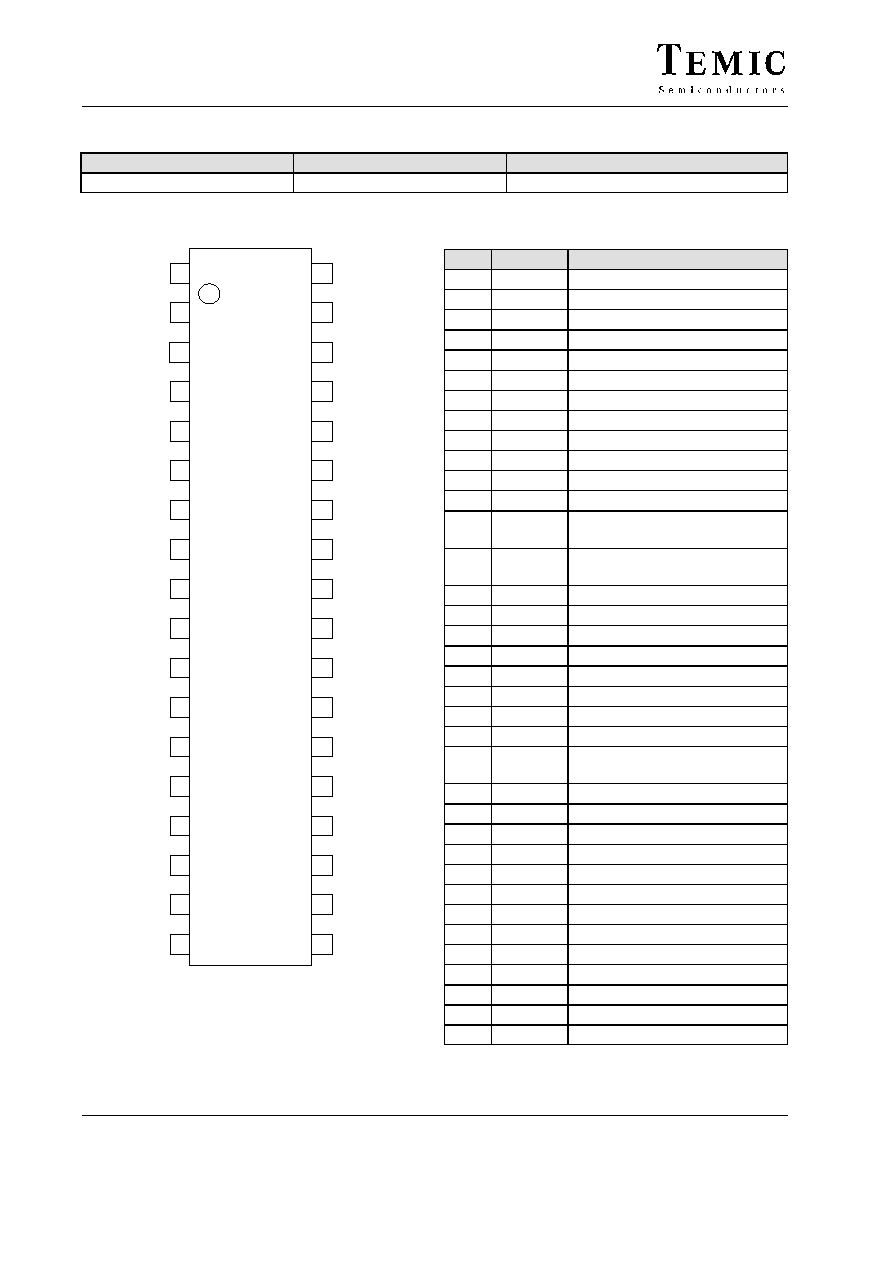
Block Diagram
1:2
N
22
21
15
16
MUX
90
�
V
Ref
Modulator
7
8
I NI
Q NQ
PU
NMIXOMIXO
32
33
23
35
36
2
1
Mixer
PFD
Charge
pump
14
13
31
28
10
11
27
26
RF
NRF
VSP
CPO
VS2
MDO
NMDO
ND
NND
RD
NRD
MC
GND2
CPCL
CPCH
14891
VS1 GND1
5
6
LO
4
3
MDLO
NMDLO
34
25
30
GND3
24
NMIXLO
29
VS3
12
GNDP
17
1:2
R
PUMIX MIXLO
Mode control
Figure 1. Block diagram
U2896B
Rev. A1, 18-Sep-98
2 (13)
Preliminary Information
Ordering Information
Extended Type Number
Package
Remarks
U2896B-MFCG3
SSO36
Taped and reeled
Pin Description
1
2
3
4
5
6
7
8
9
10
11
12
13
14
15
16
17
18
19
20
21
22
36
35
34
33
32
31
30
29
28
27
26
25
24
23
14892
I
NI
MDLO
NMDLO
GND1
VSI
1)
MDO
NMDO
SUB
VSP
CPO
GNDP
CPCL
CPCH
RD
NRD
MC
n.c.
VS3
1)
GND3
RF
NRF
VS2
1)
GND2
MIXO
NMIXO
MIXLO
PUMIX
NQ
Q
NMIXLO
PU
ND
NND
n.c.
n.c.
Figure 2. Pinning
Pin
Symbol
Function
���
���
1
����
����
I
�����������
�����������
In-phase base band-input
���
���
2
����
����
NI
�����������
�����������
Complementary to I
���
���
3
����
����
MDLO
�����������
�����������
I/Q-modulator LO input
���
���
4
����
����
NMDLO
�����������
�����������
Complementary to MDLO
���
���
5
����
����
GND1
�����������
�����������
Ground
���
6
����
VS1
1)
�����������
Supply I/Q modulator
���
���
7
����
����
MDO
�����������
�����������
I/Q modulator
���
���
8
����
����
NMDO
�����������
�����������
Complementary to MDO
���
���
9
����
����
SUB
�����������
�����������
Substrate, connected to GND
���
���
10
����
����
VSP
�����������
�����������
Supply charge pump
���
���
11
����
����
CPO
�����������
�����������
Charge pump output
���
���
12
����
����
GNDP
�����������
�����������
Ground
���
���
13
����
����
CPCL
�����������
�����������
Charge pump current control
GSM1800
���
�
�
�
���
14
����
�
��
�
����
CPCH
�����������
�
���������
�
�����������
Charge pump current control
GSM900
���
���
15
����
����
RD
�����������
�����������
R-divider input
���
���
16
����
����
NRD
�����������
�����������
Complementary to RD
���
���
17
����
����
MC
�����������
�����������
Mode control
���
18
����
n.c.
�����������
Not connected
���
���
19
����
����
n.c.
�����������
�����������
Not connected
���
���
20
����
����
n.c.
�����������
�����������
Not connected
���
���
21
����
����
NND
�����������
�����������
Complementary to ND
���
���
22
����
����
ND
�����������
�����������
N-divider input
���
�
�
�
���
23
����
�
��
�
����
PU
�����������
�
���������
�
�����������
Power-up. whole chip, except
mixer
���
���
24
����
����
NMIXLO
�����������
�����������
Complementary to MIXLO
���
���
25
����
����
MIXLO
�����������
�����������
Mixer LO input
���
���
26
����
����
GND2
�����������
�����������
Ground
���
���
27
����
����
VS2
1)
�����������
�����������
Supply (MISC)
���
���
28
����
����
NRF
�����������
�����������
Complementary to RF
���
���
29
����
����
RF
�����������
�����������
Mixer RF input
���
���
30
����
����
GND3
�����������
�����������
Ground
���
31
����
VS3
1)
�����������
Supply mixer
���
���
32
����
����
NMIXO
�����������
�����������
Complementary to MIXO
���
���
33
����
����
MIXO
�����������
�����������
Mixer output
���
���
34
����
����
PUMIX
�����������
�����������
Power-up mixer
���
���
35
����
����
NQ
�����������
�����������
Complementary to Q
���
���
36
����
����
Q
�����������
�����������
Quad-phase base-band input
1)
Between the Pins VS1, VS2 and VS3 the allowed
maximum voltage is
200 mV
U2896B
Rev. A1, 18-Sep-98
3 (13)
Preliminary Information
Absolute Maximum Ratings
Parameters
Symbol
Value
Unit
�������������
�������������
Supply voltage VS1, VS2, VS3
��������
��������
V
VS#
���������
���������
v V
VSP
�����
�����
V
�������������
�������������
Supply voltage charge pump VSP
��������
��������
V
VSP
���������
���������
5.5
�����
�����
V
�������������
�������������
Voltage at any input
��������
��������
V
Vi#
���������
���������
�0.5
v V
Vi#
v V
VS#
+5.5
�����
�����
V
�������������
�������������
Current at any input / output pin
except CPC
��������
��������
| I
I#
| | I
O#
|
���������
���������
2
�����
�����
mA
�������������
�������������
CPC output currents
��������
��������
| I
CPC
|
���������
���������
5
�����
�����
mA
�������������
�������������
Ambient temperature
��������
��������
T
amb
���������
���������
�20 to +85
�����
�����
�
C
�������������
�������������
Storage temperature
��������
��������
T
stg
���������
���������
�40 to +125
�����
�����
�
C
Operating Range
Parameters
Symbol
Value
Unit
�������������
�������������
Supply voltage
��������
��������
V
VS#
���������
���������
2.7 to 5.5
�����
�����
V
�������������
�������������
Supply voltage
��������
��������
V
VSP
���������
���������
2.7 to 5.5
�����
�����
V
�������������
�������������
Ambient temperature
��������
��������
T
amb
���������
���������
�20 to +85
�����
�����
�
C
Thermal Resistance
Parameters
Symbol
Value
Unit
�������������
�������������
Junction ambient SSO36
��������
��������
R
thJA
���������
���������
130
�����
�����
K/W
Electrical Characteristics
V
S
= 2.7 to 5.5 V, T
amb
= �20
�
C to +85
�
C, final test at 25
�
C
Parameters
Test Conditions / Pin
Symbol
Min.
Typ.
Max.
Unit
��������������������������������
��������������������������������
DC supply
��������
��������
Supply voltages VS#
���������
���������
V
VS1
= V
VS2
= V
VS3
�����
�����
V
VS#
�����
�����
2.7
���
���
����
����
5.5
����
����
V
��������
��������
Supply voltage VSP
���������
���������
�����
�����
V
VSP
�����
�����
V
VS#
� 0.3
���
���
����
����
5.5
����
����
V
��������
��������
Supply current I
VS1
���������
���������
Active (V
PU
= VS)
�����
�����
I
VS1A
�����
�����
���
���
17
����
����
22
����
����
mA
��������
pp y
���������
Standby (V
PU
= 0)
�����
I
VS1Y
�����
���
����
20
����
mA
��������
��������
Supply current I
VS2
���������
���������
Active (V
PU
= VS)
�����
�����
I
VS2A
�����
�����
���
���
17
����
����
22
����
����
mA
��������
��������
pp y
���������
���������
Standby (V
PU
= 0)
�����
�����
I
VS2Y
�����
�����
���
���
����
����
20
����
����
mA
��������
��������
Supply current I
VS3
���������
���������
Active (V
PUMIX
= VS)
�����
�����
I
VS3A
�����
�����
���
���
13
����
����
17
����
����
mA
��������
��������
pp y
���������
���������
Standby (V
PUMIX
= 0)
�����
�����
I
VS3Y
�����
�����
���
���
����
����
30
����
����
mA
��������
�
������
�
��������
Supply current I
VSP
1)
���������
�
�������
�
���������
Active
(V
PU
= VS, CPO open)
�����
�
���
�
�����
I
VSPA
�����
�
���
�
�����
���
�
�
�
���
1.4
����
�
��
�
����
1.8
����
�
��
�
����
mA
��������
���������
Standby (V
PU
= 0)
�����
I
VSPY
�����
���
����
20
����
mA
��������������������������������
��������������������������������
N & R divider inputs ND, NND & RD, NRD
��������
��������
N:1 divider frequency
���������
���������
50-
W source
�����
�����
f
ND
�����
�����
100
���
���
����
����
600
����
����
MHz
��������
��������
R:1 divider frequency
���������
���������
50-
W source
�����
�����
f
RD
�����
�����
100
���
���
����
����
600
����
����
MHz
��������
��������
Input impedance
���������
���������
Active & standby
�����
�����
Z
RD
, Z
ND
�����
�����
1
���
���
����
����
����
����
k
W
��������
��������
Input sensitivity
���������
���������
50-
W source
�����
�����
V
RD
, V
ND
�����
�����
5
2)
���
���
����
����
200
����
����
mV
rms
��������
��������
Input capacitance
���������
���������
Active & standby
�����
�����
C
RD
, C
ND
�����
�����
���
���
����
����
0.5
����
����
pF
1)
Mean value, measured with F
ND
= 151 MHz, F
RD
= 150 MHz, current vs. time, see page 6, figure 3
2)
For optimized noise performance this voltage level may be higher

U2896B
Rev. A1, 18-Sep-98
4 (13)
Preliminary Information
Electrical Characteristics (continued)
V
S
= 2.7 to 5.5 V, T
amb
= �20
�
C to +85
�
C, final test at 25
�
C
Parameters
Test Conditions / Pin
Symbol
Min.
Typ.
Max.
Unit
��������������������������������
��������������������������������
Phase-frequency detector (PFD)
��������
�
������
�
��������
PFD operation
��������
�
������
�
��������
f
ND
= 600 MHz, N = 2
f
RD
= 600 MHz, R = 2
�������
�
�����
�
�������
f
PFD
���
�
�
�
���
50
����
�
��
�
����
����
�
��
�
����
300
����
�
��
�
����
MHz
��������
��������
Frequency comparison
only
4)
��������
��������
f
ND
= 600 MHz, N = 2
f
RD
= 450 MHz, R = 2
�������
�������
f
FD
���
���
����
����
����
����
400
����
����
MHz
��������������������������������
��������������������������������
I/Q modulator baseband inputs I, NI & Q, NQ
��������
�
������
�
��������
DC voltage
��������
�
������
�
��������
Referred to GND
�������
�
�����
�
�������
V
I,
V
NI,
V
Q,
V
NQ
���
�
�
�
���
1.35
����
�
��
�
����
VS1/2
����
�
��
�
����
VS1/2
+ 0.1
����
�
��
�
����
V
��������
��������
MD_IQ
��������
��������
Frequency range
�������
�������
f
IO
���
���
0
����
����
����
����
1
����
����
MHz
��������
��������
AC voltage
5)
��������
��������
Referred to GND
�������
�������
AC
I,
AC
NI,
AC
Q,
AC
NQ
���
���
����
����
200
����
����
����
����
mV
pp
��������
��������
AC voltage
��������
��������
Differential (preferres)
�������
�������
AC
DI,
AC
DQ
���
���
����
����
400
����
����
����
����
mV
pp
��������������������������������
��������������������������������
I/Q modulator LO input MDLO
��������
��������
MDLO
��������
��������
Frequency range
�������
�������
f
MDLO
���
���
100
����
����
����
����
450
����
����
MHz
��������
��������
Input impedance
��������
��������
Active & standby
�������
�������
Z
MDLO
���
���
����
����
3
����
����
����
����
k
W
��������
��������
Input level
��������
��������
50-
W source
�������
�������
P
MDLO
���
���
�14
����
����
�11
����
����
�5
����
����
dBm
��������������������������������
��������������������������������
I/Q modulator outputs MDO, NMDO
��������
��������
DC current
��������
��������
V
MDO
, V
NMDO
= VS
�������
�������
I
MDO
, I
NMDO
���
���
����
����
0.8
����
����
����
����
mA
��������
Internal pull-up resistor
��������
�������
R
MDO
, R
NMDO
���
����
615
����
����
W
��������
��������
Voltage compliance
��������
��������
V
MDO
, V
NMDO
= VC
�������
�������
VC
MDO
, VC
NMDO
���
���
V
S
� 0.7
����
����
����
����
5.5
����
����
V
��������
�
������
�
��������
MDO output level
(differential)
��������
�
������
�
��������
615
W to VS
6)
1.5 pF external load
�������
�
�����
�
�������
P
MDO
���
�
�
�
���
40
����
�
��
�
����
����
�
��
�
����
60
����
�
��
�
����
mV
rms
��������
��������
Carrier suppression
6)
��������
��������
�������
�������
CS
MDO
���
���
�32
����
����
�35
����
����
����
����
dBc
��������
��������
Sideband suppression
6)
��������
��������
�������
�������
SS
MDO
���
���
�35
����
����
�40
����
����
����
����
dBc
��������
��������
IF spurious
6)
��������
��������
f
LO
�
3
f
mod
�������
�������
SP
MDO
���
���
����
����
�50
����
����
�45
����
����
dBc
��������
Noise
6)
��������
@ 400 kHz off carrier
�������
N
MDO
���
����
����
�115
����
dBc/Hz
��������
��������
Frequency range
��������
��������
�������
�������
f
MDO
���
���
100
����
����
����
����
450
����
����
MHz
��������������������������������
��������������������������������
Mixer (900 MHz)
��������
��������
RF input level
��������
��������
900 MHz
�������
�������
P9
RF
���
���
�23
����
����
����
����
�17
����
����
dBm
��������
��������
Output resistance
��������
��������
�������
�������
R
MIXO
, R
NMIXO
���
���
����
����
650
����
����
����
����
W
��������
�
������
�
��������
LO-spurious at
RF/NRF port
��������
�
������
�
��������
@ P9
MIXLO
= �10 dBm
@ P9
RF
= �15 dBm
�������
�
�����
�
�������
SP9
RF
���
�
�
�
���
����
�
��
�
����
����
�
��
�
����
�40
����
�
��
�
����
dBm
��������
MIXLO input level
��������
0.05 to 2 GHz
�������
P9
MIXLO
���
�22
����
����
�12
����
dBm
��������
��������
MIXO
��������
��������
Frequency range
�������
�������
f
MIXO
���
���
50
����
����
����
����
450
����
����
MHz
��������
�
������
�
��������
Output level
7)
differen-
tial
��������
�
������
�
��������
@ P9
MIXLO
= �15 dBm
�������
�
�����
�
�������
P9
MIXO
���
�
�
�
���
����
�
��
�
����
80
����
�
��
�
����
����
�
��
�
����
mV
rms
��������
��������
Carrier suppression
��������
��������
@ P9
MIXLO
= �15 dBm
�������
�������
CS9
MIXO
���
���
�20
����
����
����
����
����
����
dBc
4)
PFD can be used as a frequency comparator until 300 MHz for loop acquisition
5)
Single-ended operation (complementary baseband input is AC-grounded) leads to reduced linearity
(degrading suppression of odd harmonics)
6)
With typical drive levels at MDLO- & I/Q-inputs
7)
�1 dB compression point C = 1.5 pF to GND
U2896B
Rev. A1, 18-Sep-98
5 (13)
Preliminary Information
Electrical Characteristics (continued)
V
S
= 2.7 to 5.5 V, T
amb
= �20
�
C to +85
�
C, final test at 25
�
C
Parameters
Test Conditions / Pin
Symbol
Min.
Typ.
Max.
Unit
��������������������������������
��������������������������������
Mixer (1900 MHz)
��������
��������
Output resistance
��������
��������
������
������
R
MIXO
, R
NMIXO
����
����
����
����
650
����
����
����
����
W
��������
��������
RF input level
��������
��������
0.5 to 2 GHz
������
������
P19
RF
����
����
�23
����
����
����
����
�17
����
����
dBm
��������
�
������
�
��������
LO-spurious at
RF/NRF ports
��������
�
������
�
��������
@ P19
MIXLO
= �10 dBm
@ P19
RF
= �15 dBm
������
�
����
�
������
SP19
RF
����
�
��
�
����
����
�
��
�
����
����
�
��
�
����
�40
����
�
��
�
����
dBm
��������
MIXLO input level
��������
0.05 to 2 GHz
������
P19
MIXLO
����
�22
����
����
�12
����
dBm
��������
��������
MIXO
��������
��������
������
������
����
����
����
����
����
����
����
����
��������
�
������
�
��������
Output level
8)
differen-
tial
��������
�
������
�
��������
@ P19
MIXLO
= �17 dBm
������
�
����
�
������
P19
MIXO
����
�
��
�
����
����
�
��
�
����
70
����
�
��
�
����
����
�
��
�
����
mVrms
��������
��������
Carrier suppression
��������
��������
@ P19
MIXLO
= �17 dBm
������
������
CS19
MIXO
����
����
�20
����
����
����
����
����
����
dBc
��������������������������������
��������������������������������
Charge-pump output CPO (V
VSP
= 5 V; V
CPO
= 2.5 V)
��������
��������
Pump-current pulse
��������
��������
R
CPCH
9)
= 4.7 k
������
������
| I
CPO_H
|
����
����
1.4
����
����
2
����
����
2.6
����
����
mA
��������
p
p
��������
R
CPCL
10)
= 2.4 k
������
| I
CPO_L
|
����
3
����
4
����
5
����
mA
��������
�
������
�
��������
Sensivity to V
VSP
|
DI
CPO
I
CPO
|
|
DV
VSP
V
VSP
|
������
�
����
�
������
S
ICPO
����
�
��
�
����
����
�
��
�
����
����
�
��
�
����
0.1
����
�
��
�
����
�
��������
�
������
�
�
������
�
��������
V
CPO
voltage range
��������
�
������
�
�
������
�
��������
| I
CPO
| degradation <
10%
(V
VSP
= 2.7 V to 5 V)
������
�
����
�
�
����
�
������
V
CPO
����
�
��
�
�
��
�
����
0.5
����
�
��
�
�
��
�
����
����
�
��
�
�
��
�
����
V
VSP
�0.6
����
�
��
�
�
��
�
����
V
��������������������������������
��������������������������������
Mode control
��������
��������
Sink current
��������
��������
V
MC
= VS
������
������
I
MC
����
����
����
����
60
����
����
����
����
mA
��������������������������������
Power-up input PU (power-up for all functions, except mixer)
��������
�
������
�
��������
Settling time
��������
�
������
�
��������
Output power within 10%
of steady state values
������
�
����
�
������
S
PU
����
�
��
�
����
����
�
��
�
����
5
����
�
��
�
����
10
����
�
��
�
����
ms
��������
��������
High level
��������
��������
Active
������
������
V
PUH
����
����
2.0
����
����
����
����
����
����
V
��������
��������
Low level
��������
��������
Standby
������
������
V
PUL
����
����
0
����
����
����
����
0.4
����
����
V
��������
��������
High-level current
��������
��������
Active, V
PUH
= 2.2 V
������
������
I
PUH
����
����
����
����
����
����
70
����
����
mA
��������
��������
Low-level current
��������
��������
Standby, V
PUL
= 0.4 V
������
������
I
PUL
����
����
�1
����
����
����
����
20
����
����
mA
��������������������������������
Power-up input PUMIX (power-up for mixer only)
��������
�
������
�
��������
Settling time
��������
�
������
�
��������
Output power within 10%
of steady state values
������
�
����
�
������
t
setl
����
�
��
�
����
����
�
��
�
����
5
����
�
��
�
����
10
����
�
��
�
����
ms
��������
��������
High level
��������
��������
Active
������
������
V
PUMIXH
����
����
2.0
����
����
����
����
����
����
V
��������
��������
Low level
��������
��������
Standby
������
������
V
PUMIXL
����
����
0
����
����
����
����
0.4
����
����
V
��������
��������
High-level current
��������
��������
Active, V
PUMIXH
= 2.2 V
������
������
I
PUMIXH
����
����
0.1
����
����
����
����
70
����
����
mA
��������
��������
Low-level current
��������
��������
Standby,
V
PUMIXL
= 0.4 V
������
������
I
PUMIXL
����
����
�1
����
����
����
����
20
����
����
mA
8)
� 1 dB compression point C = 1.5 pF to GND
9)
R
CPCH
: external resistor to GND for charge-pump current control (MODE 1, 5, only Pin 14 active)
10)
R
CPCL
: external resistor to GND for charge-pump current control (MODE 2, 3, 4, only Pin 13 active)

U2896B
Rev. A1, 18-Sep-98
6 (13)
Preliminary Information
Supply Current of the Charge Pump I
VSP
vs. Time
Due to the pulsed operation of the charge pump, the
current into the charge-pump supply pin VSP is not
constant. Depending on I (see figure 5) and the phase
difference at the phase detector inputs, the current I
VSP
over time varies. Basically, the total current is the sum of
the quiescent current, the charge-/discharge current, and
� after each phase comparison cycle � a current spike (see
figure 3).
Internal current |I
CPC
| vs. R
CPC
R
CPC
|I
CPCO
|
19.2 k
W
0.5 mA
9.6 k
W
1 mA
4.8 k
W
2 mA
2.4 k
W
4 mA
(typical values)
Down
Up
2.5 I
CPCO
1.5 I
CPCO
I
CPCO
I
�I
CPCO
t
t
14913
I
VSP
I
CPO
Figure 3. Supply current of the charge pump
Mode Selection
The device can be programmed to different modes via an external resistor RMODE (including short, open) from Pin
MC to VS2. The mode is distinguished from specific N-, R-divider ratios, and the polarity of the charge-pump selection.
Mode Selection
N-Divider
R-Divider
CPO Current Polarity
4)
Application
CPCH
active
CPCL
active
Mode
Resistance
between Pin MC
and Pin VS2
f
n
< f
R
1)
f
n
> f
R
1)
1
0 (<50
W)
1:1
1:1
sink
source
t.b.d.
x
2
2.7 k
W (
�
5%)
1:1
1:1
source
sink
t.b.d.
x
3
10 k
W (
�
5%)
1:1
2:1
source
sink
t.b.d.
x
4
47 k
W (
�
5%)
2:1
2:1
source
sink
PCN/ PCS
2)
x
5
(> M
W)
2:1
2:1
sink
source
GSM
3)
x
1)
Frequencies referred to PFD input
2)
LO frequencies below VCO frequency
3)
LO frequencies above VCO frequency
4
)
Sink current into Pin CPO. Source: current out from Pin CPO.

U2896B
Rev. A1, 18-Sep-98
7 (13)
Preliminary Information
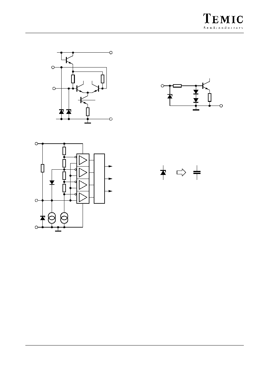
Equivalent Circuits at the IC's Pins
I,Q
NI, NQ
2230
2230
VS1
MDO
NMDO
GND
Baseband inputs
LO input
Output
14893
MDLO
V
Bias_MDLO
V
Ref_input
V
Ref_MDLO
V
Ref_output
2 x 615
W
Figure 4. I/Q modulator
14894
NRF
RF input
890
890
1 k
LO output
1.6 k
1.6 k
1 k
RF
MIXLO
MIXO
VS3
GND
V
Bias_RF
V
Ref_RF
V
Bias_LO
V
Ref_LO
650
W
650
W
NMIXO
Output
Figure 5. Mixer
14896
Ref
up
Ref
n
down
I
I
4
4
VSP
CPO
GNDP
n
= Transistor with an emitter area�factor of "n"
V
Ref
CPCL
CPCH
n
Figure 6. Charge pump
U2896B
Rev. A1, 18-Sep-98
8 (13)
Preliminary Information
14897
GND
2 k
2 k
ND/RD
NND/NRD
VS2
V
Ref_div
Figure 7. Dividers
14899
GND
PU, PUMIX
20 k
Figure 8. Power-up
14898
GND
N�divider
2x
60
�
A
Logic
R�divider
MUX
MC
VS2
Figure 9. Mode control
14900
C (U)
0.5 pF @ 2 V
C (U) is a non-linear junction capacitance
Figure 10. ESD-protection diodes
U2896B
Rev. A1, 18-Sep-98
9 (13)
Preliminary Information
Application Hints
Interfacing
For some of the baseband ICs it may be necessary to
reduce the I/Q voltage swing so that it can be handled by
the U2896B. In those cases, the following circuitry can be
used.
14901
I
I
R2
R1
R1
R2
R1
R1
NI
Q
NQ
Baseband IC
NI
Q
NQ
U2896B
C
C
Figure 11. Interfacing the U2896B to I/Q baseband circuits
Due to a possible current offset in the differential base-
band inputs of the U2896B the best values for the carrier
suppression of the I/Q modulator can be achieved with
voltage driven I/NI-, and Q/NQ-inputs. A value of
R
source
= R2/2*R
S
v 1.5 kW should be realized. R
S
is the
sum of R1 (above drawing) and the output resistance of
the baseband IC.
Mode Control
14895
R
Mode1
R
Mode2
VS2
MC
U2896B
VS2
MC
U2896B
R
Mode
VS2
MC
U2896B
VS2
MC
U2896B
R
Mode
36 k
or
10 k
R
Mode
a) any single mode
b) any 2 modes
c) any mode
& mode 5
d) mode 5 & mode 3 or mode 4
Figure 12. Application examples for programming
different modes

U2896B
Rev. A1, 18-Sep-98
10 (13)
Preliminary Information
Test Circuit
1
2
3
4
5
6
7
8
9
10
11
12
13
14
15
16
17
18
19
20
21
22
36
35
34
33
32
31
30
29
28
27
26
25
24
23
14903
450 mV
pp
V5
R1
R2
V4
1.35V
R3
200MHz
�10dBm
C1
C2
C3
3V
3V, 5V
C4
R4
V7
1.5V
R5
R6
R7
200.1MHz
�15dBm
C5
C6
R8
R9
R10
450 mV
pp
V2
R11
R12
V3
1.35V
C16
R14
200MHz
�15dBm
C15
3V
C14
R13
1100MHz
�15dBm
C13
3V
C12
C11
900MHz
�15dBm
C10
C9
3V
C7
C8
3V
3V
U2896B
n.c.
n.c.
n.c.
Figure 13. Test circuit
U2896B
Rev. A1, 18-Sep-98
11 (13)
Preliminary Information
Application Circuit for DCS1800 (1710 � 1785 MHz)
1
2
3
4
5
6
7
8
9
10
11
12
13
14
15
16
17
18
19
20
21
22
36
35
34
33
32
31
30
29
28
27
26
25
24
23
14904
R1
R2
2nd LO
C2
C3
C4
3V
3V, 5V
C5
R4
R5
R6
C9
C10
R9
R10
C20
C19
C18
C17
3V
C16
C15
C14
C13
3V
U2896B
C1
R3
Baseband
�10dBm
3V
R7
C11
L2
L1
C8
C6
C7
C12
R8
Baseband
880 to 915MHz
�20dBm
1710 to 1785MHz
�15dBm
1st LO
C29
L3
Tuning voltage
3V
VCO
3V
n.c.
n.c.
n.c.
Figure 14. Application circuit
Measurements
Modulation-Loop Settling Time
As valid for all PLL loops the settling time depends on
several factors. The following figure is an extraction from
measurements performed in an arrangement like the
application circuit. It shows that a loop settling time of a
few
ms can be achieved.
Modulation Spectrum & Phase Error
CPC: 1 k
to GND
CPC `open'
Vertical: VCO tuning voltage 1 V/Div
Horizontal: Time 1
ms/Div

U2896B
Rev. A1, 18-Sep-98
12 (13)
Preliminary Information
Package Information
13047
Package SSO36
Dimensions in mm
technical drawings
according to DIN
specifications
9.6
9.1
1.3
0.15
0.05
0.2
0.5
8.45
36
19
1
18
4.5
4.3
6.6
6.3
0.12
5.6
5.2

U2896B
Rev. A1, 18-Sep-98
13 (13)
Preliminary Information
Ozone Depleting Substances Policy Statement
It is the policy of TEMIC Semiconductor GmbH to
1. Meet all present and future national and international statutory requirements.
2. Regularly and continuously improve the performance of our products, processes, distribution and operating systems
with respect to their impact on the health and safety of our employees and the public, as well as their impact on
the environment.
It is particular concern to control or eliminate releases of those substances into the atmosphere which are known as
ozone depleting substances ( ODSs ).
The Montreal Protocol ( 1987 ) and its London Amendments ( 1990 ) intend to severely restrict the use of ODSs and
forbid their use within the next ten years. Various national and international initiatives are pressing for an earlier ban
on these substances.
TEMIC Semiconductor GmbH has been able to use its policy of continuous improvements to eliminate the use of
ODSs listed in the following documents.
1. Annex A, B and list of transitional substances of the Montreal Protocol and the London Amendments respectively
2 . Class I and II ozone depleting substances in the Clean Air Act Amendments of 1990 by the Environmental
Protection Agency ( EPA ) in the USA
3. Council Decision 88/540/EEC and 91/690/EEC Annex A, B and C ( transitional substances ) respectively.
TEMIC Semiconductor GmbH can certify that our semiconductors are not manufactured with ozone depleting
substances and do not contain such substances.
We reserve the right to make changes to improve technical design and may do so without further notice.
Parameters can vary in different applications. All operating parameters must be validated for each customer
application by the customer. Should the buyer use TEMIC products for any unintended or unauthorized
application, the buyer shall indemnify TEMIC against all claims, costs, damages, and expenses, arising out of,
directly or indirectly, any claim of personal damage, injury or death associated with such unintended or
unauthorized use.
TEMIC Semiconductor GmbH, P.O.B. 3535, D-74025 Heilbronn, Germany
Telephone: 49 ( 0 ) 7131 67 2594, Fax number: 49 ( 0 ) 7131 67 2423