
U3500BM
Preliminary Information
Rev. A3, 20-May-98
1 (17)
Cordless Telephone Signal Processor
Description
The programmable cordless phone signal processor
includes all necessary low frequency parts such as
microphone- and earphone amplifier, compander, pre-
emphasis, deemphasis, scrambler, data management,
power-supply management, as well as RF receiving parts
such as IF converter, FM demodulator. RSSI and low
noise amplifier.
Several gains and mutes in transmit and receive direction
are controlled by serial bus while compander, pre- and
deemphasis and scrambler can be bypassed.
Features
RF Receiver Part
D Low-noise amplifier
D IF converter
D FM demodulator
D RSSI
Low Frequency Part
D Symmetrical input of microphone amplifier
D Symmetrical output of earpiece amplifier
D Compander
D Pre- and deemphasis
D Scrambler
D Data management
D Power-supply management
D Serial bus
Application: CT0
Block Diagram
LOG
MIXO
IFIN2
IFIN1
DACO
Scrambler
frequency
Expander
REC
Oscillator
11.15 MHz
LNA
MIXIN
MIXGND
LOIN
LNAIN
RGND
LNAO
VBATT
D/A
Battery low
detector
LPF
C
D
Serial
Bus
LPF
TGAIN
ADJ.2
Limiter
Preem
TGAIN
ADJ.1
Compressor
IFAMP
Demodulator
RGAIN
ADJ
LPF
LPF
Deem
MIC
Scrambler
frequency
RXO
ETC
EXIN
RECO2
RECO1
RXDAT
TXDAT
MIC1
MIC2
MICO
COIN
VCC
TXO
GND
CTC
14678
LPF
Divider
Figure 1. Block diagram
U3500BM
Rev. A3, 20-May-98
Preliminary Information
2 (17)
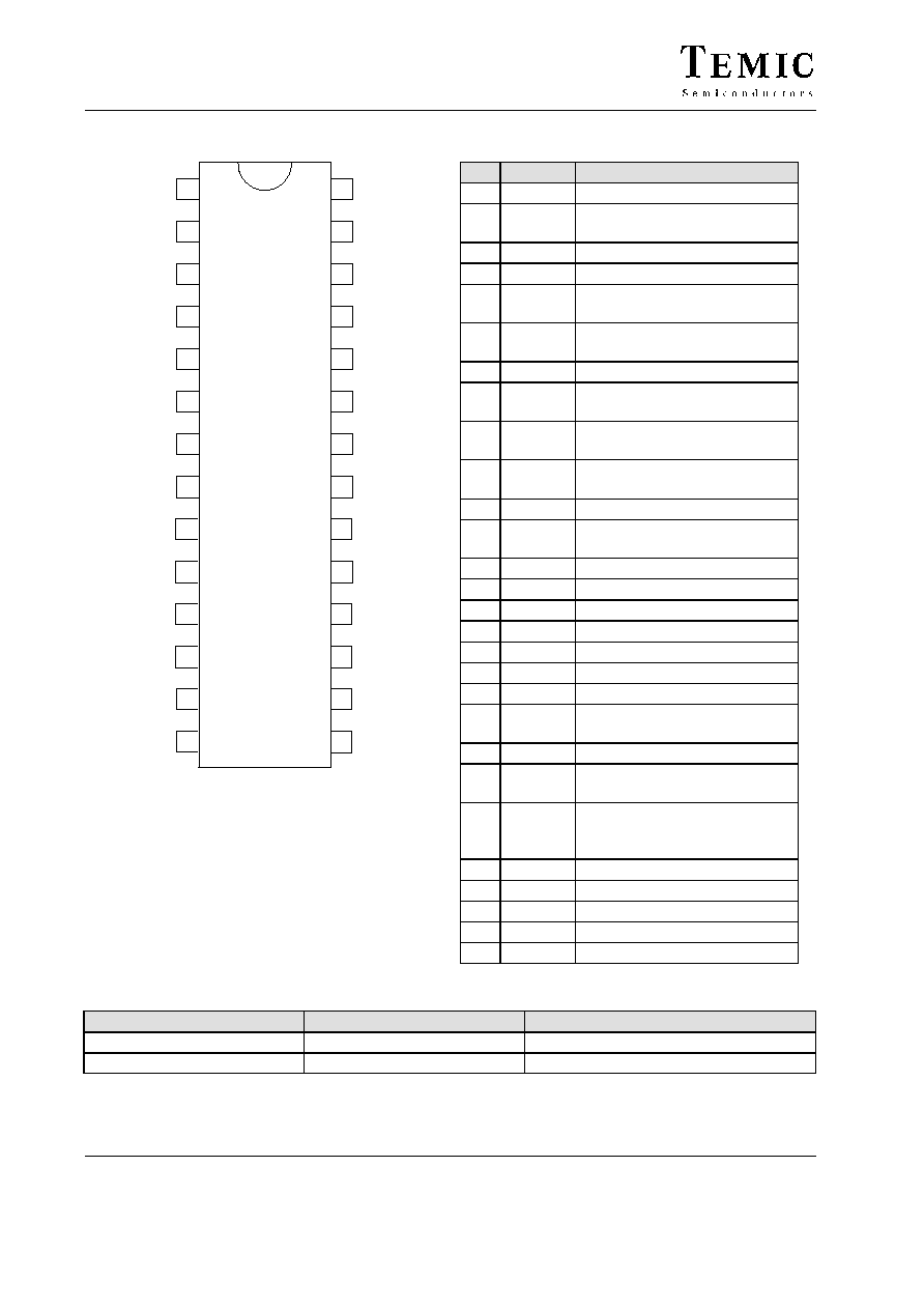
Pin Description
1
2
3
4
5
6
7
8
10
9
27
22
21
20
18
19
17
12
11
28
25
26
23
24
MIC1
GND
RXO
RECO2
RECO1
EXIN
MICO
MIC2
ETC
COIN
CTC
TXO
VCC
LOIN
VBATT
LNAO
RGND
LNAIN
C
DACO
MIXGND
D
RXDAT
TXDAT
16
15
14
13
96 11791
IFIN2
IFIN1
MIXIN
MIXO
Figure 2. Pinning
Pin
Symbol
Function
1
TXO
Transmit section analog output
2
CTC
Compressor time constant
control analog output
3
COIN
Compressor analog input
4
MICO
Microphone amplifier output
5
MIC2
Non-inverting input of
microphone amplifier
6
MIC1
Inverting input of microphone
amplifier
7
GND
LF analog/ digital ground
8
RXO
Intermediate receive analog
output
9
RECO2
Symmetrical output of receive
amplifier
10
RECO1
Symmetrical output of receive
amplifier
11
EMN
Expander analog input
12
ETC
Expander time constant control
analog output
13
IFIN2
Symmetrical IF amplifier input
14
IFIN1
Symmetrical IF amplifier input
15
MIXO
Mixer output
16
MIXIN
Mixer input
17
MIXGND IF amplifier and mixer ground
18
LNAIN
Low-noise amplifier input
19
RGND
Low-noise amplifier ground
20
LNAO
Low-noise amplifier output/
External LO input
21
VBATT
Battery supply
22
LOIN
Local oscillator input
(11.15 MHz)
23
VCC
Supply-voltage output for
peripherals and internal supply
of digital part
24
DACO
D/A comparator output
25
C
Clock input of serial bus
26
D
Data input of serial bus
27
RXDAT
Receive data digital output
28
TXDAT
Transmit data input
Order Information
Extended Type Number
Package
Remarks
U3500BM-BFL
SO28
U3500BM-BFLG3
SO28
Taped and reeled

U3500BM
Preliminary Information
Rev. A3, 20-May-98
3 (17)
Absolute Maximum Ratings
Parameters
Symbol
Value
Unit
Supply voltage
V
Batt
, V
CC
5.5
V
Junction temperature
T
j
+125
∞
C
Ambient temperature
T
amb
≠25 to +75
∞
C
Storage temperature
T
stg
≠50 to +125
∞
C
Power dissipation
T
amb
= 60
∞
C
P
tot
1
W
Thermal Resistance
Parameters
Symbol
Value
Unit
Junction ambient
SO28
R
thJA
120
K/W
Electrical Characteristics
Test conditions (unless otherwise specified): V
Batt
= V
CC
= 3.6 V, T
amb
= +25
∞
C
Parameters
Test Conditions / Pins
Symbol
Min.
Typ.
Max.
Unit
Fig.
Current consumption
ERX2
ELNA
ERXHF
ERX1
ERXO
EEA
EDEE
ETX
EPREE
0
0
0
0
0
0
0
0
0
Operating voltage range
3.1
3.6
5.2
V
Inactive mode
V
Batt
= 2.9 V
30
60
80
mA
Standby mode
100
120
mA
RX waiting for RSSI
ELNA = ERXHF = 1
1.7
2.5
3.4
mA
RX waiting for data
ELNA = ERXHF = ERX1 = 1
1.45
1.9
2.45
mA
Operating current, RX and
TX completely active
ERX2 = ELNA = ERXHF =
ERX1 = ERXO = EEA=
EDEE = GDEM = ETX = 1
4.5
6.5
9.5
mA
Low noise amplifier (LNA) f = 41.4 MHz, input level = ≠50 dBm
Supply current
0.8
1
1.2
mA
3
Input impedance
160
200
240
W
3
Output impedance
40
80
120
W
3
Gain
f = 50 MHz
20
23
26
dB
3
Noise figure
Bandwidth = 1 MHz
4
5
dB
3
1-dB input compression
point
≠27
≠24
dBm
3
Third-order input intercept
point
f = 41.4 MHz
f = 41.4125 MHz
Input level = ≠60 dBm
≠15
≠12
dBm
3
Frequency range FRF
20
50
MHz
3

U3500BM
Rev. A3, 20-May-98
Preliminary Information
4 (17)
Parameters
Test Conditions / Pins
Symbol
Min.
Typ.
Max.
Unit
Fig.
Receiver
IF mixer, f = 10.7 MHz
Input resistance
2000
3000
4000
W
4
Input capacitance
2.5
3
3.5
pF
4
Output impedance
1200
1500
1800
W
4
Gain GVMIX
Input level 7 mV
rms
G
MIX
13
15
17
dB
4
Input compression point
≠17
dBm
4
Third-order input intercept
point
≠9
dBm
4
Carrier breakthrough from
internal LO (11.15 MHz) to
IF output
300
mV
rms
4
Carrier breakthrough from
internal LO (11.15 MHz) to
RF input
10
mV
rms
4
IF amplifier: RSSI
Input resistance
1.6
2
2.5
k
W
5
RSSI-sensitivity
VIF = 0
mV
rms
starting from 0 increase RSSI-
level until mean of sampled
signal at DACO is
v 0.2
RSSI-level = CON0
VIF = 25.4
mV
rms,
f = 450 kHz
increase RSSI level again
until mean of sampled signal
at DACO is
v0.2.
RSSI-level = CON1
RSSI-sensitivity =
CON1≠CON0
1
5
RSSI-input voltage
dynamic range
60
65
dB
5
RSSI-level number of
programmable steps
*)
127
5
RSSI-level step size in the
logarithmic region
0.35
0.46
0.6
dB
5
*) RSSI Level Programming (Typical Values)
Input Voltage VIF (
mV
rms
)
RSSI Level (Decimal)
0
5
25.4
8
42.4
14
424
54
4240
97
42400
111

U3500BM
Preliminary Information
Rev. A3, 20-May-98
5 (17)
Parameters
Test Conditions / Pins
Symbol
Min.
Typ.
Max.
Unit
Fig.
RF demodulator
fIF = 450 kHz, fMOD = 1 kHz, V
IF
= 500
mV
rms
BSCR
EDEE
GRX0
GRX1
GRX2
GRX3
ERX1
ERXO
ERX2
1
0
1
1
1
0
1
1
1
Recovered audio
GDEM = 0,
DfFM = 2.5 kHz
GDEM = 1,
DfFM = 5.0 kHz
0.4
0.4
0.8
0.8
1.6
1.6
Vpp
Vpp
6
Recovered audio output
voltage drop
V
Batt
= 3.1 to 5.2 V
≠1
+1
dB
6
AM rejection ratio
30% AM
30
35
dB
6
RX audio
Change of RX0 signal
deemphasis bypass
EDEE = 0
≠0.5
0
0.5
dB
6
Gain adjust range
12
15
17
dB
6
Gain adjust step
0.8
1
1.2
dB
6
Output signal vs. frequency
relative to 1 kHz (0 dB)
deemphasis bypassed
100 Hz
300 Hz
1800 Hz
3200 Hz
4100 Hz
≠7.5
≠2.0
≠1.3
≠0.8
≠6.5
≠1.0
≠0.3
0.2
≠5.5
0
0.7
1.2
≠60
dB
6
Output signal vs. frequency
relative to 1 kHz (0 dB)
deemphasis enable
EDEE = 1
100 Hz
300 Hz
1800 Hz
3200 Hz
4100 Hz
≠0.7
3.7
≠5.7
≠10
0.3
4.7
≠4.7
≠9.0
1.3
5.7
≠3.7
≠8.0
≠66
dB
6
Total harmonic distortion
DFM = 250 Hz
DFM = 2.50 kHz
3.5
3.5
%
%
6
Audio mute
DFM = 2.5 kHz, ERXO = 0
ERX1 = 0, ERX2 = 0
65
dB
6
Output impedance
100
W
Expander
EEA
GEA0
GEA1
GEA2
GEA3
GEA4
1
0
0
0
1
1
Gain reference level
VEXIN = ≠10 dBV
rms
G
OREC
11
13
15
dB
7
Change of gain when
expander is bypassed
BCOMP = 1
≠0.5
0.5
dB
7
Gain tracking
VEXIN = ≠20 dBV
rms
VEXIN = ≠30 dBV
rms
VEXIN = ≠35 dBV
rms
VEXIN = ≠40 dBV
rms
≠21
≠41
≠53
≠50
≠60
≠19
≠39
≠47
dB
7
Input impedance
9.5
14.5
k
W
7
Gain change vs. supply
voltage
V
Batt
= 3.1 to 5.2 V
≠0.5
0.5
dB
7
Attack time
VEXIN = step
≠20 dBV
rms
≥ ≠14 dBV
rms
,
measure time after step, when
output voltage has 0.75 times
the final value
t
f
16
ms
7
Release time
VEXIN = step
14 dBV
rms
≥ ≠20 dBV
rms
,
measure time after step, when
output voltage has 1.5 times of
the final value
t
f
16
ms
7