Ad
ro
ni
c
Co
m
po
ne
nt
s
G
m
bH
U3550BM
Preliminary Information
Rev. A2, 10-Sep-98
1 (25)
Low-Power FM Transmitter / Synthesizer System 26 to 50 MHz
Description
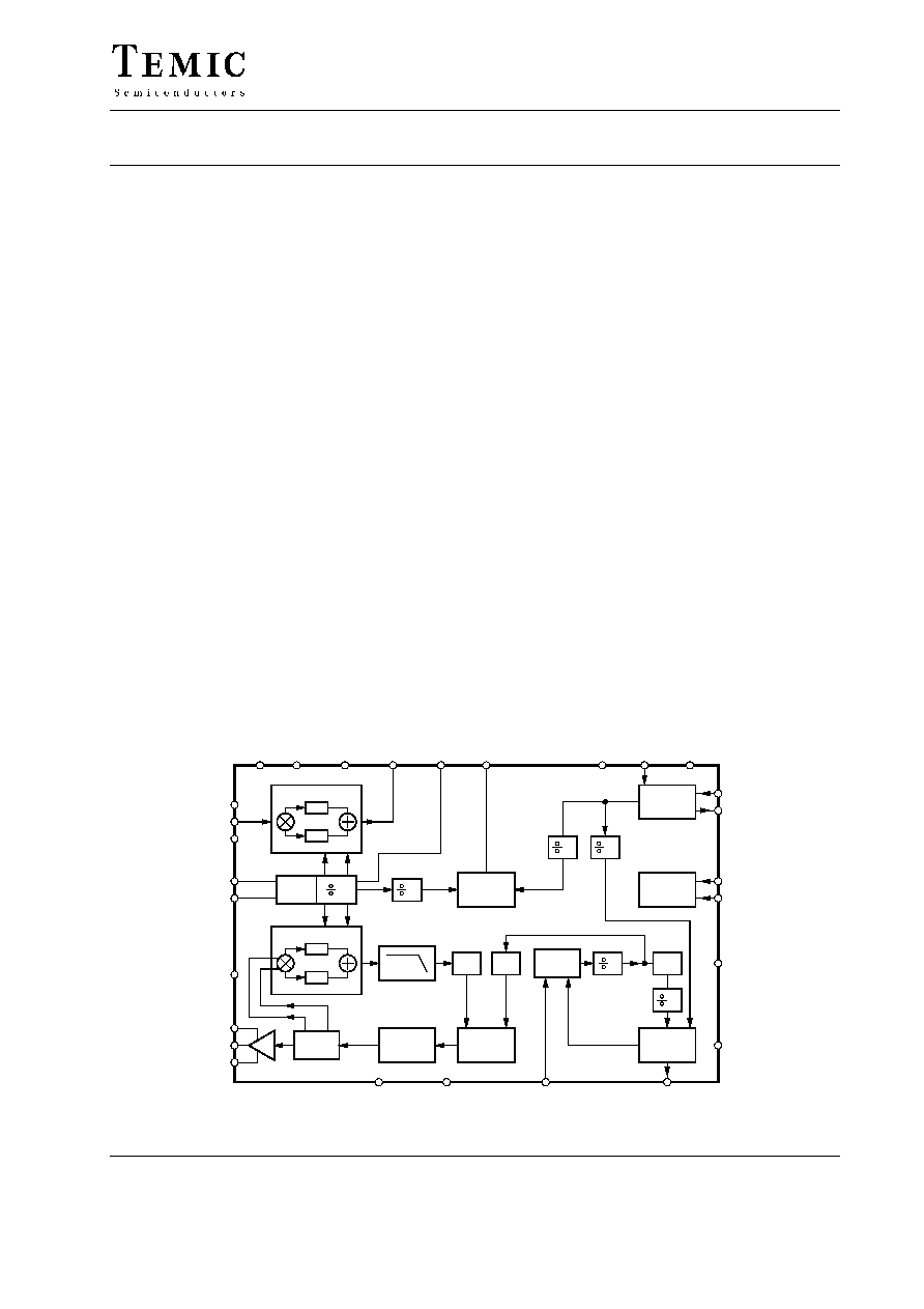
The U3550BM is a radio-frequency IC for analog
cordless telephone applications in the 26/50-MHz band
(CTO standard). The IC performs full duplex communi-
cation. The transmitting and receiving frequency depends
on whether the IC is used in the handset or in the base
station.
The U3550BM's frequency converter consists of an FM
transmitter with switchable output power and receiver
Mixer 1 in the same unit. A two-wire bus interface can be
used for frequency control as well as for switching the
transmitter's power amplifier and the receiver. Fine
frequency adjustment of the reference crystal oscillator is
programmable.
The receive part is designed for a double-conversion
architecture. The incoming radio-frequency signal will
be filtered and amplified before reaching the first mixer.
At this stage, the RF signal will be converted down to the
first intermediate frequency (10.7 MHz) by using a local
adjustable oscillator (VCO3). The frequency of this
oscillator is controlled by the PLL.
The transmitter part contains two PLL-controlled VCOs.
The frequency modulation is accomplished by
superposing the incoming audio signal on the first PLL
control voltage. In this system, the frequency is a product
of mixing VCO1 with local oscillator (VCO3). The FM-
modulated carrier is amplified by external power
amplifier before entering the output filter and the antenna
connector.
Features
D All PLLs and most of the oscillators are integrated
D All functions and channel selection controllable by
serial bus
D Receiver Mixer 1 with integrated image rejection
D Up to 25 channels selectable depending on CT0
standard
D Integrated oscillator circuit with external crystal
(11.15 MHz)
D Programmable carrier-modulation frequency
Application
D CT0 (USA, France, Spain, Netherlands, Portugal,
Korea, Taiwan, New Zealand, China)
D Narrowband voice and data transmitting / receiving
systems
Block Diagram
Mixer 1
+ 45
≠ 45
VCO 3
sin
cos
sin
cos
Mixer 2
+ 45
≠ 45
Phase
comparator
VCO 2
D 1
D 2
Loop
filter
VCO 1
Phase
comparator
D 3
N
Phase
comparator
Serial BUS
interface
Oscillator
interface
20
11.15 MHz
10.7 MHz
VCC
MIXIN
MIXVB
LO1
LO2
VTX
RFOVB
RFO
RFOGND
AGND
MODIN
MLF
XCK
MCKO
C
D
LFGND
VBAT
MIXO
PCLO
LOGND
MCKA
OSCGND
13280
557.5 KHz
DELGND
DELVB
OSCVDD
GREF
VSS
2
K
2
P
Figure 1. Block diagram
Ad
ro
ni
c
Co
m
po
ne
nt
s
G
m
bH
U3550BM
Rev. A2, 10-Sep-98
Preliminary Information
2 (25)
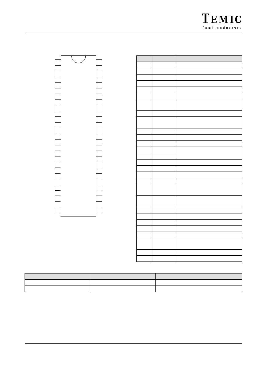
Pin Description
1
2
3
4
5
6
7
8
10
9
23
18
17
16
14
15
13
12
11
24
21
22
19
20
OSCVDD
DELVB
11623
DELGND
GREF
MIXIN
MIXVB
OSCGND
XCK
MIXO
C
D
MCKO
MLF
VBAT
AGND
VTX
RFOVB
RFO
MODIN
LFGND
RFOGND
MCKA
VSS
VCC
27
28
25
26
LO1
LO2
LOGND
PCLO
Figure 2. Pinning
Pin
Symbol
Function
1
MCKO
Clock output for peripherals
2
D
Data input of serial bus
3
C
Clock line of serial bus
4
OSCGND Oscillator ground
5
XCK
Oscillator input (11.15 MHz)
6
OSCVDD Oscillator supply input
7
DELVB
Phase correction VCO3 supply
input
8
DELGND Phase correction VCO3 ground
9
GREF
Voltage reference for internal
current sources
10
MIXIN
Mixer input
11
MIXVB
Mixer-supply input
12
MIXO
Mixer output
13
LO1
Tank elements for LO are
14
LO2
connected to these pins
15
PCLO
Phase comparator PLL3 output
16
LOGND
VCO3 ground
17
RFOGND RF transmit output ground
18
RFO
RF transmit output
19
RFOVB
Power-supply input of RF
transmit output buffer
20
VTX
Power-supply output of RF
external power amplifier
21
AGND
Analog ground
22
VBAT
Power supply of analog part
23
MLF
Modulator loop filter
24
LFGND
Modulator loop-filter ground
25
MODIN
Modulator input signal
26
MCKA
Peripheral-clock output
adjustment
27
VSS
Digital ground
28
VCC
Power supply of digital part
Order Information
Extended Type Number
Package
Remarks
U3550BM-AFL
SO28
U3550BM-AFLG3
SO28
Taped and reeled
Ad
ro
ni
c
Co
m
po
ne
nt
s
G
m
bH
U3550BM
Preliminary Information
Rev. A2, 10-Sep-98
3 (25)
VCO Adjustments
To be able to use a wide VCO frequency range
(i.e., VCO2 = 26.3 to 49.9 MHz), VCO1 and VCO2 have
a rough adjust and a fine adjust to increase the frequency
range given by the phase comparator.
The 4 rough adjusts for VCO1 and VCO2 (3 used in
VCO1) are correlated to the country setting. For each
country, there are two sets of VCO rough adjust settings,
one for the base and one for the handset (see tables
Channel Frequencies, Dividers and Country Settings).
To achieve the adaption to the various country standards,
there is a fine adjust with 32 steps for VCO1 and VCO2.
These fine adjusts can be set manually (for test purposes)
or by the automatically mode. Theoretically, the indicator
of the change (increase/ decrease when the voltage of the
phase comparator is too high) is selectable. The program-
ming value `1', however, is necessary.
Setting normal conditions VCO1:
EAFA1 = 1, automatic fine adjust VCO1 enabled
SAFA1 = 1, sign of auto fine adjustment VCO1 = 1.
Setting for VCO2 is identical.
For VCO3, there is no internal adjustment.
Speed-up of the Modulator Loop Filter
To obtain a fast locking time for the modulator loop, there
is a precharge and a speed-up mode for the external loop
filter.
During receive mode (VCO3 enabled, VCO1 disabled),
the modulator loop filter is precharged to 1.25 V.
During the first 30 ms after enabling VCO1, the modu-
lator phase comparator is in speed-up mode. In this mode,
the current of the phase comparator which charges the
loop filter is much larger than in normal mode. The
duration of the speed-up mode depends on the number of
oscillator clock cycles.
Duration Adjustment of the
Anti-Backlash Signals
The phase comparators of the modulator- and the mixer-
loop have a 2-bit adjustment for the duration of the up-
and down pulses when the loop is locked (anti-backlash).
Best results can be achieved by setting all the bits
(AMOD[2:1], AMIX[2:1]) to 0.
Adjustment of the Modulator Gain
To fulfill all requirements of the various countries, three
conversion gains of the modulator are selectable by the
bits GMOD[1:0].
For country settings, see tables Channel Frequencies,
Dividers and Country Settings. For the ranges, see tabel
Electrical Characteristics (RF transmitter).
Clock-Output Divider Adjustment
The MCKO pin is a clock output derived from the crystal
oscillator. It can be used to drive a microprocessor or
other remote components and thereby reduces the number
of crystals required.
The crystal oscillator frequency can be divided by an
integer value: 1, 2, 3, 4, 6 or switched off.
The divider value is adjusted by an analog level on the
MCKA pin.
Table 1 shows the clock-output value on MCKO for
different divider values and the corresponding level
required on MCKA.
Crystal oscillator = 11.15 MHz.
Table 1. Clock-output values
Level on MCKA
0 to 7% V
CC
13% to 27% V
CC
33% to 47% V
CC
53% to 67% V
CC
73% to 87% V
CC
93% to V
CC
Level on MCKA
for V
CC
= 3.6 V
0 to 0.25
0.47 to 0.97
1.19 to 1.69
1.91 to 2.41
2.63 to 3.13
3.35 to 3.6
Corresponding
divider
X
6
4
3
2
1
Corresponding
clock on MCKO
(MHz)
No output
1.858
2.7875
3.716
5.575
11.15

Ad
ro
ni
c
Co
m
po
ne
nt
s
G
m
bH
U3550BM
Rev. A2, 10-Sep-98
Preliminary Information
4 (25)
Frequency Synthesis
Phase
comparator
N
Loop
filter
1)
Modulator loop
2)
Mixer loop
3)
Local oscillator (LO) loop
3)
VCO 3
Phase
comparator
Loop
filter
VCO 2
D1
2)
D2
VCO 1
2
D3
Loop
filter
Q
223
Phase
comparator
f
mod
557.5 kHz
1)
96 11627
2
f
Ref3
f
LO
K
f
Ref
11.15 MHz
P+
f
Ref1
=
Figure 3.
Modulator Loop and Mixer Loop Dividers
D1
D2
D3
f
Ref2
(MHz)
f
mod
(MHz)
France
4
8
2
1.075
4.3
Spain
2
8
4
0.9
1.8
Netherlands
2
8
4
0.9
1.8
Portugal
2
8
4
0.625
1.25
USA (channels 1 to 10)
8
8
1
0.955
7.64
USA (new channels)
6
6
1
0.943
5.66
Taiwan
8
8
1
0.9625
7.70
New Zealand
4
8
2
0.5875
4.70
Korea
8
8
1
0.955
7.64
For France, Spain, Netherlands, Portugal, Taiwan and New Zealand, f
Ref2
and f
mod
do not change when the channel changes. For USA
and Korea is valid: f
Ref2
and f
mod
are varying according to the channel number. For all countries, f
Ref2
and f
mod
are identical for base
set and handset.
Reference Frequency Dividers for Local Oscillator
K
0
= 4460
K
1
= 2230
K
2
= 1784
K
3
= 1115
K
4
= 892
K
5
= 446
f
Ref3
=
2.5 kHz
f
Ref3
=
5 kHz
f
Ref3
=
6.25 kHz
f
Ref3
=
10 kHz
f
Ref3
=
12.5 kHz
f
Ref3
=
25 kHz
Ad
ro
ni
c
Co
m
po
ne
nt
s
G
m
bH
U3550BM
Preliminary Information
Rev. A2, 10-Sep-98
5 (25)
Modulator PLL
The fractional divider has been chosen to increase
reference the frequency of the modulator PLL.
557.5 kHz
+ f
mod
P
)
Q
223
P: integer part of the fractional divider
Q: fractional part of the fractional divider
Q
+ 223
f
mod
557.5 kHz
≠P
223
+ 557.7 kHz
2.5 kHz
The frequency step 2.5 kHz is a fraction of the reference
frequency 557.5 kHz
≥
Qx (P
) 1) ) (223≠Q)P
223
+ P )
Q
223
For each comparison cycle (f
Ref1
= 557.5 kHz), the accu-
mulator content is incremented by the Q value and the
divider divides by the P value. When the accumulator
value reaches or exceeds 223, the divider divides by the
value (P + 1). Then, the accumulator holds the excess
value (accumulator value ≠ 223). After 223 cycles, the
correct division is executed.
Local Oscillator PLL
f
Ref3
+
f
LO
N
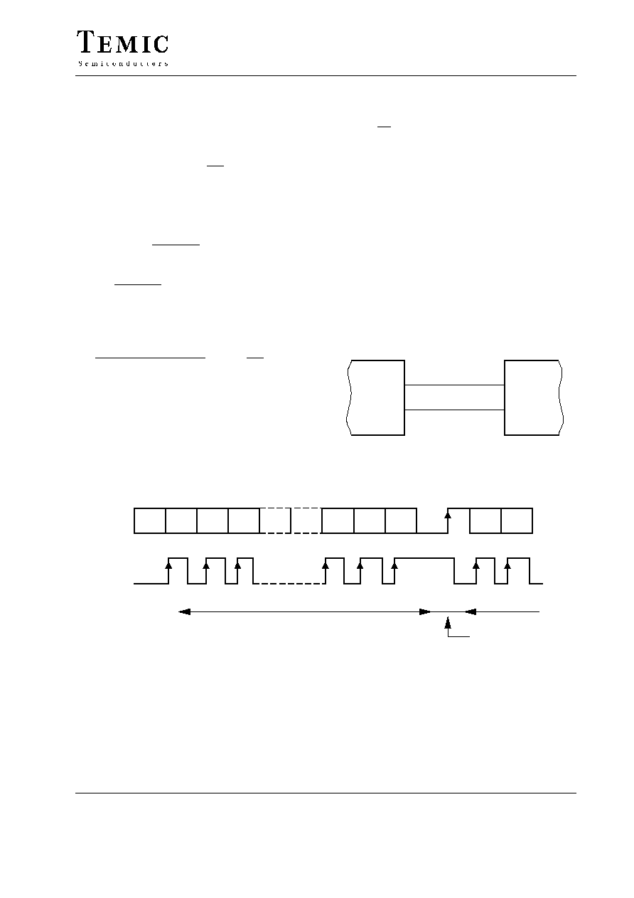
Serial Bus Interface
The circuit is remoted by an external microcontroller
through the serial bus.
The data is a 12-bit word:
A0 ≠ A3: address of the destination register (0 to 15)
D0 ≠ D7: contents of register
The data line must be stable when the clock is high and
data must be shifted serially.
After a 12-clock period, the transfer to the destination
register is generated (internally) by a low-to-high
transition of the data line when the clock is high.
Micro-
processor
D
Clock
C
96 11787
Data
Figure 4.
Word transmission
Transfer condition
2nd word
1st word
Data
(D)
Clock
(C)
D0
D1
D2
A1
A2
A3
13279
A0
Figure 5. Serial bus transmission