
U3760MB
Rev. A3, 19-Feb-98
1 (19)
Low-Voltage Standard Telephone Circuit
Description
TEMIC's low-voltage telephone circuit, U3760MB,
performs all the speech and line interface functions
required in an electronic telephone set tone ringer, pulse
and DTMF dialing with redial.
Electrostatic sensitive device.
Observe precautions for handling.
Features
Speech Circuit
D Adjustable dc characteristic
D Symmetrical input of microphone amplifier
D Receiving amplifier for dynamic or piezo-electric
earpieces
D Automatic line-loss compensation
D Selectable flashing duration by key pad
D Pause function
D Last number redial up to 32 digits
D Standard low-cost 3.58-MHz crystal or ceramic
resonator
Dialer
D DTMF / pulse switchable
D Pulse dialing 66/33 or 60/40 for 10 ppS and 20 ppS or
DTMF dialing selectable by pins
D Key tone
Tone Ringer
D Two-tone ringer
D Adjustable volume
D RC oscillator
D Adjustable threshold
Benefits
D Low number of external components
D High quality through one-IC solution
D One IC for all standards
Ordering Information
Extended Type Number
Package
Remarks
U3760MB-MSD
SDIP40
U3760MB-MFN
SSO44
U3760MB-MFNG3
SSO44
Taped and reeled
U3760MB
2 (19)
Rev. A3, 19-Feb-98
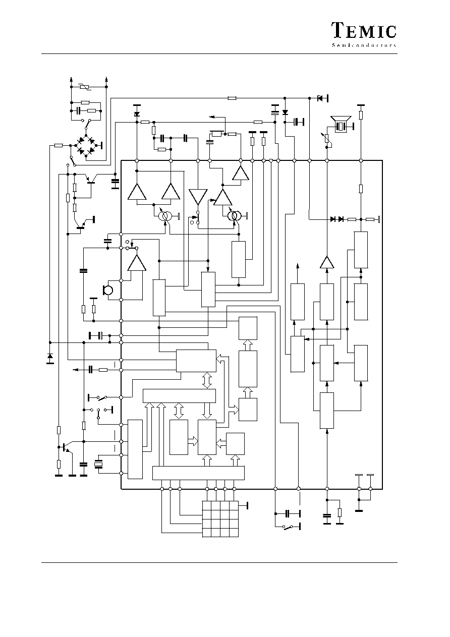
Block Diagram / Applications
¡¡
Sidetone amplifier
Receiver attenuation
Control function
Control function
RECIN
ST
MIC2
MIC1
Mute control
Supply current
regulator
AGC current
generator
≠
+
Microphone
amplifier
Pulse control logic
VDD1
Location
latch
Read ≠ write
counter
C
o
n
t
r
o
l
l
o
g
i
c
K e y b o a r d
i n t e r f a c e
AGC
RDC
MODE
Comparator
with hysteresis
Clock signal
oscillator
Divider
T
one signal generator
Divider
Supply
Power
-on-reset
Bandgap reference
HKS
VI
390
VRIAC
Ring
Ti
p
100
OUT
THA
XT
C1
C2
C3
R1
R2
R3
R4
RCK
GND1
RAM
8176
MICO
TIN
DP
HKS
HKS
Clock
generator
D/A
converter
Data
latch & decoder
ROW
& column
programmable
counter
T
ransmit
amplifier
Receiving amplifier
RECO1
VL
XT
MFO
2
13
F1
45
6
F2
78
9
F
3
*/T
0
#
R/P
VRING
BM
KT
RECO2
PRIV
ACY
EP
VDD2
GND2
220 k
1
M
470 k
BC546
100 n
3.58 MHz
47 n
5 k
220
18 k
22 k
220 n
MPSA42
3 k
33 k
220 k
220 k
1
13 V
330
680
470
2.4 k
3 n 3
47 n
2.2
100
1.8 k
12 k
39
10
28 V
10 k
10 k
47 n
1 n
150 k
m
m
m
m
¡¡
¡¡
5M
1 W
100 n
VBG
MUTE
m
EP
75V
1 W
2 n 2
CL
2N5401
5 V
1
Figure 1.

U3760MB
Rev. A3, 19-Feb-98
3 (19)
SDIP40
SSO44
1
2
3
4
5
6
7
8
9
10
11
12
13
14
15
16
17
18
19
20
40
39
38
37
36
35
34
33
32
31
30
29
28
27
26
25
24
23
22
21
R4
R3
R2
DP
MODE
BM
HKS
VBG
VDD 1
OUT
RCK
VRING
VRIAC
AGC
THA
ST
PRIVACY
RECO 1
RECO 2
C2
C3
KT
XT
GND 1
MFO
XT
MIC 1
MICO
VL
RDC
TIN
VI
MUTE
n.c.
RECIN
U3760MB
C1
GND 2
MIC 2
R1
VDD 2
10181
1
2
3
4
5
6
7
8
9
10
11
12
13
14
15
16
17
18
19
20
21
22
44
43
42
41
40
39
38
37
36
35
34
33
32
31
30
29
28
27
26
25
24
23
R4
R3
R2
n.c.
MODE
BM
HKS
n.c.
VDD 1
OUT
RCK
VRING
VRIAC
AGC
THA
ST
PRIVACY
RECO 1
RECO 2
C2
C3
n.c.
n.c.
n.c.
KT
XT
MFO
GND 1
MICO
VL
RDC
TIN
VI
MUTE
VBG
RECIN
U3760MB
C1
XT
GND 2
MIC 1
R1
VDD 2
10180
MIC 2
DP

U3760MB
4 (19)
Rev. A3, 19-Feb-98
Pin Description
PD means protection device
SDIP40
SSO44
Symbol
Function
Configuration
1
1
C1
Keyboard input
C1
PD
2
2
C2
C2
PD
PD
3
3
C3
C3
PD
15
4, 5,
6, 35
n.c.
Not connected
4
7
KT
Key tone signal output generated
for all keys in pulse dialing mode
(except Flash + Redial) with a fre-
quency of about 1240 Hz and dura-
tion about 50 ms
KT
5
8
XT
A built-in inverter provides
oscillation with an inexpensive
3.579545-MHz crystal or ceramic
resonator
XT
PD
6
9
XT
resonator
XT
PD
40P
40P
7
10
MFO
Output of DTMF
DTMF output frequency
Specified
Actual
Error
(HZ)
(Hz)
(%)
R1
697
699
+0.28
R2
770
766
≠0.52
R3
852
848
≠0.47
R4
941
948
+0.74
C1
1209
1216
+0.57
C2
1336
1332
≠0.30
C3
1477
1472
≠0.34
MFO
9
12
GND 1
Ground 1 connected with ground 2
8
11
GND 2
U3760MB
Rev. A3, 19-Feb-98
5 (19)
Configuration
Function
Symbol
SSO44
SDIP40
10
13
MIC 1
Inverting input of microphone
amplifier
MIC1
VI
MIC2
1V
PD
50K
11
14
MIC 2
Non-inverting input of microphone
amplifier
VI
MIC2
1V
PD
50K
12
15
MICO
Transmit pre-amp output which is
normally capacitively coupled to
Pin TIN
VI
1V
MICO
PD
16K
13
16
VL
Positive supply voltage input to the
device. The current through this
pin is modulated by the transmit
signal.
VL
RDC
PD
PD
16V
14
17
RDC
An external resistor (1 W) is
required from this pin to GND to
control the dc input impedance of
the circuit. It has a nominal value
of 39
W for low-voltage operation.
Values up to 100
W may be used to
increase the available transmit
output voltage swing at the expense
of low-voltage operation.
RDC
AGC
VL
PD
PD
16
18
TIN
Input to the line output driver am-
plifier. Transmit AGC is applied to
this stage.
1V
TIN
PD
5.6K
16V
17
19
V
I
This internal voltage bias line must
be connected to VL via an external
resistor, R
B
, which dominates the
ac input impedance of the circuit
and should be 680
for 600-
W
input impedance or 1.2 k
for a
900-
input impedance.
VI
PD
16V