 | –≠–ª–µ–∫—Ç—Ä–æ–Ω–Ω—ã–π –∫–æ–º–ø–æ–Ω–µ–Ω—Ç: U3762MB | –°–∫–∞—á–∞—Ç—å:  PDF PDF  ZIP ZIP |
U3762MB
Preliminary Information
Rev. A1, 15-Sep-98
1 (23)
Universal Telephone IC
* All Functions Integrated
Description
TEMIC's low-voltage telephone circuit U3762MB
performs all the speech and line interface functions
required in an electronic telephone set, the tone ringer, the
pulse and DTMF dialing with redial. Operation below
15 mA is possible with reduced performance (no dialing).
Features
Speech Circuit
D Adjustable DC characteristic
D Symmetrical input of microphone amplifier
D Receiving amplifier for dynamic or
piezo-electric earpieces
D Automatic line-loss compensation
D Anti-clipping in transmit direction
Dialer
D DTMF / pulse switchable
D Pulse dialing 66/33 or 60/40 or DTMF dialing
selectable by pin
D Flashing time duration 98 ms
D Pause function
D Last number redial up to 32 digits
D Standard low-cost crystal 3.57 MHz or
ceramic resonator
D Key tone
Tone Ringer
D 2-tone ringer
D Adjustable volume
D RC oscillator
D Adjustable threshold
Benefits
D Low number of external components
D High quality through one IC solution
Ordering Information
Type
Package
Remarks
U3762MB-MFN
SSO44
U3762MB-MFNG3
SSO44
Taped and reeled

U3762MB
Rev. A1, 15-Sep-98
Preliminary Information
2 (23)
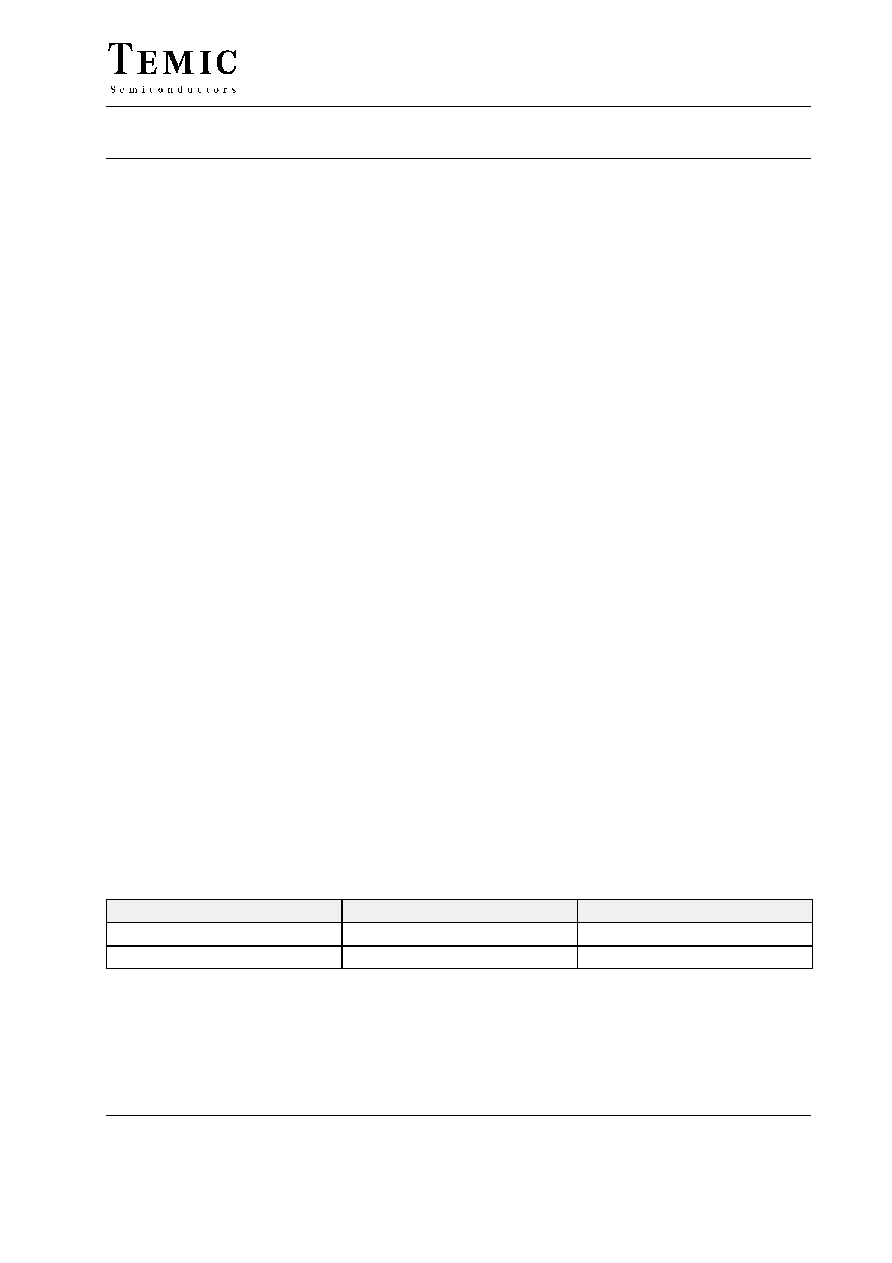
Block Diagram / Applications
Mask
470
m
F
PRIND
MODE
to key
board
matrix
HKS
ROW
& column
programmable
counter
Clock
generator
RAM
Location
latch
Read ≠ write
counter
Control
logic
Pulse
control
logic
Supply
current
regulator
Key≠
board
inter≠
face
XT
3.58 MHz
KT
Earth
DP
Data
latch &
decoder
D /
A
converter
Mute
control
VDD
HFI
HFO
TEST
Handsfree
control
logic
MFO
MIC1
MIC2
≠
+
Micro≠
phone
amplifier
MICO
TIN
220 nF
18 k
W
220 nF
MPSA42
3 k
W
33 k
W
HKS
220 k
W
XT
2.2 nF
CL
2.4 k
W
680
W
T
ransmit
amplifier
Control
function
Sidetone
amplifier
Control
function
AGC
current
generator
Receiver
attenuation
Receiving
amplifier
VL
ST
3.3 nF
RECIN
47 nF
RECO1
2.2
m
F
100
W
RECO2
330
W
1
m
F
470
W
13 V/
1 W
5 M
W
Ti
p
Ring
75 V
5.1 V
Clock signal
oscillator
Divider
Supply
Power on reset
T
one signal
generator
Divider
Bandgap
reference
Comparator
with hysteresis
AGC
12 k
W
RDC
39
W
300
W
1.8 k
W
VI
100
m
F
MUTE
MFIND
VRING
10
m
F
OUT
10 k
W
THA
10 k
W
VRIAC
C1
C2
C3
C4
R1
R2
R3
R4
12
3
45
6
78
9
F
*/T
0
#
R/P
1 nF
RCK
150 k
W
2N5401
HKS
1 W
14912
100 k
W
2.2
m
F
CLIM
470 nF
1 k
W
VI
Figure 1.

U3762MB
Preliminary Information
Rev. A1, 15-Sep-98
3 (23)
Pin Description
1
2
3
4
5
6
7
8
9
10
11
12
13
14
15
16
17
18
19
20
21
22
44
43
42
41
40
39
38
37
36
35
34
33
32
31
30
29
28
27
26
25
24
23
R4
R3
R2
Mask
MODE
KT
HKS
n.c.
VDD
OUT
RCK
VRING
VRIAC
AGC
THA
ST
CLIM
RECO 1
RECO 2
C2
C3
C4
Earth
HFI
HFO
XT
MFO
GND
MICO
VL
RDC
TIN
VI
MUTE
PRIND
RECIN
U3762MB
C1
XT
MFIND
MIC 1
R1
TEST
14835
MIC 2
DP
SSO44

U3762MB
Rev. A1, 15-Sep-98
Preliminary Information
4 (23)
Pin
Symbol
Function
Configuration
1
C1
Keyboard input
C1
VDD
VDD
2
C2
VDD
PD
3
C3
VDD
C2≠C4
4
C4
VDD
PD = Protection Device
5
Earth
Earth key ( 604 ms high pulse, 1 s pause)
VDD
EARTH
PD
6
HFI
Input with 200 k
W pull-down resistor.
HFI triggers HFO with each LH edge.
HFI
VDD
VDD
PD
200K
7
HFO
Output will be toggled by each LH edge at
HFI.
HFO
VDD
PD
8
9
XT
XT
A built-in inverter provides oscillation with an
inexpensive 3.579545-MHz crystal or ceramic
resonator
XT
VDD
VDD
VDD
VDD
XT
PD
PD
10
MFO
Output of DTMF
DTMF output frequency
Specified
Actual
Error
(Hz)
(Hz)
(%)
R
1
697
699
+0.28
R
2
770
766
≠0.52
R
3
852
848
≠0.47
R
4
941
940
≠0.10
C
1
1209
1216
+0.57
C
2
1336
1332
≠0.30
C
3
1477
1472
≠0.34
MFO
VDD
VDD
PD

U3762MB
Preliminary Information
Rev. A1, 15-Sep-98
5 (23)
Configuration
Function
Symbol
Pin
11
MFIND
Output switches to low being in temporary
DTMF mode. Reset by on hook condition.
VDD
MFIND
PD
MFIND
12
GND
Ground
13
14
MIC 1
MIC 2
Inverting input of microphone amplifier
Non-inverting input of microphone amplifier
MIC2
VI
VI
MIC1
PD
PD
1V
1V
50K
50K
15
MICO
Transmit pre-amp output which is normally
capacitively coupled to Pin TIN
VI
1V
MICO
PD
16K
16
VL
Positive supply voltage input to the device.
The current through this pin is modulated by
the transmit signal.
VL
RDC
PD
PD
16V
17
RDC
An external resistor (1 W) is required from
this pin to GND to control the DC input im-
pedance of the circuit. It has a nominal value
of 39
W for low-voltage operation. Values up
to 100
W may be used to increase the available
transmit output voltage swing at the expense
of low-voltage operation.
RDC
AGC
VL
PD
PD
18
TIN
Input to the line output driver amplifier.
Transmit AGC applied to this stage.
1V
TIN
PD
5.6K
16V