
U3900BM
Target Specification
Rev. A2, 25-Aug-98
1 (34)
Programmable Telephone Audio Processor
Description
The programmable telephone audio processor U3900BM
is a linear integrated circuit for use in feature phones,
answering machines, fax machines and cordless phones.
It contains the speech circuit, tone-ringer interface with
DC/DC converter, sidetone equivalent and ear-protection
rectifiers. The circuit is line-powered and contains all
components necessary for signal amplification and
adaptation to the line. The U3900BM can also be supplied
via an external power supply. An integrated voice switch
with loudspeaker amplifier enables hands-free or loud-
hearing operation. With an anti-feedback function,
acoustical feedback during loudhearing can be reduced
significantly. The generated supply voltage is suitable for
a wide range of peripheral circuits.
Features
D Speech circuit with anti-clipping
D Tone ringer interface with DC/DC converter
D Speaker amplifier with anti-distortion
D Power-supply management, regulated, unregulated
and a special supply for electret microphone
D Voice switch
D CLID + SCWID
D DTMF generator
D Switch matrix
D Line current information
D Fully programmable
D Watchdog
Benefits
D Savings of one piezoelectric transducer
D Complete system integration of analog signal
processing on one chip
D Very few external components
D Highly integrated solution
D Extremely versatile due to full programmability
Applications
Feature phone, answering machine, fax machine, speaker
phone, base station of cordless phone
14602
Speech
circuit
Voice
switch
Audio
amplifier
Serial
bus
Class
Clock
Data
Reset
MCU
DTMF
Tone
ringer
Ordering Information
Extended Type Number
Package
Remarks
U3900BM-AFN
SSO44
U3900BM-AFNG3
SSO44
Taped and reeled

U3900BM
Rev. A2, 25-Aug-98
Target Specification
2 (34)
Pin Description
1
2
3
4
5
6
7
8
9
10
11
12
13
14
15
16
17
18
19
20
21
22
44
43
42
41
40
39
38
37
36
35
34
33
32
31
30
29
28
27
26
25
24
23
TSACL
MIC2
MIC1
MIC3
TXACL
RECO2
RECO1
TLDR
INLDR
TLDT
HFTX
CEAR
CMIC
AMREC
AMPB
STO
STRC
STC
RESET
OSCOUT
SAO2
GND
VB
ES
VMPS
SENSE
IND
RECIN
CLI2
IMPA
COSC
SWOUT
VMP
INT
BCL
BDA
OSCIN
14761
VRING
SAO1
VMIC
INLDT
CLI1
ADIN
VL
Figure 1. Pinning
Pin
Symbol
Function
1
SAO1
Positive output of speaker amplifier
(single ended and push-pull operation)
2
SAO2
Negative output of speaker amplifier
(push-pull only)
3
GND
Ground, reference point for DC- and
AC signals
4
VB
Unstabilized supply voltage
5
ES
Input for external supply indication
6
VMPS
Unregulated supply voltage for the micro-
controller (via series regulator to VMP)
7
SENSE
Input for sensing the available line current
8
VL
Positive supply-voltage input to the device in
speech mode
9
IND
The internal equivalent inductance of the
circuit is proportional to the value of the
capacitor at this pin. A resistor connected to
ground may be used to adjust the DC mask.
10
RECIN
Receive amplifier input
Pin
Symbol
Function
11
ADIN
Input of A/D converter
12
CLI2
CLID input 2
13
CLI1
CLID input 1
14
VRING
Input for ringer supply
15
IMPA
Input for adjusting the ringer input impedance
16
COSC
70-kHz oscillator for ringing power converter
17
SWOUT
Output for driving the external switching
transistor
18
VMP
Regulated output voltage for supplying the
microcontroller (typ. 3.3 V/ 6 mA in speech
mode)
19
INT
Interrupt line for serial bus
20
BCL
Clock input for serial bus
21
BDA
Data line for serial bus
22
OSCIN
Input for 3.58-MHz oscillator
23
OSCOU
T Clock output for the microcontroller
24
RESET
Reset output for the microcontroller
25
STC
Input for sidetone network
26
STRC
Input for sidetone network
27
STO
Output for connecting the sidetone network
28
AMPB
Input for playback signal of answering
machine
29
AMREC
Output for recording signal of answering
machine
30
CMIC
Input for cordless telephone
31
CEAR
Output for cordless telephone
32
HFTX
Output for transmit-level detector in intercom
mode
33
TLDT
Time constant of transmit-level detector
34
INLDT
Input of transmit-level detector
35
INLDR
Input of receive-level detector
36
TLDR
Time constant of receive-level detector
37
RECO1
Positive output of the receive amplifier, also
used for sidetone network
38
RECO2
Negative output of the receive amplifier
39
TXACL
Time-constant adjustment for transmit anti-
clipping
40
MIC3
Input of hands-free microphone
41
VMIC
Reference node for microphone amplifier,
supply for electret microphone
42
MIC1
Inverting input of symmetrical microphone
amplifier with high common-mode rejection
ratio
43
MIC2
Non-inverting input of symmetrical micro-
phone amplifier with high common-mode
rejection ratio
44
TSACL
Time-constant for speaker amplifier anti-
clipping

U3900BM
Target Specification
Rev. A2, 25-Aug-98
3 (34)
Table of Contents
1
Block Diagram
4
. . . . . . . . . . . . . . . . . . . . . . . . . . . . . . . . . . . . . . . . . . . . . . . . . . . . . . . . . . . . . . . . . . . .
2
Class Function
5
. . . . . . . . . . . . . . . . . . . . . . . . . . . . . . . . . . . . . . . . . . . . . . . . . . . . . . . . . . . . . . . . . . . . .
2.1
CLID
5
. . . . . . . . . . . . . . . . . . . . . . . . . . . . . . . . . . . . . . . . . . . . . . . . . . . . . . . . . . . . . . . . . . . . . .
2.1.1
Description
5
. . . . . . . . . . . . . . . . . . . . . . . . . . . . . . . . . . . . . . . . . . . . . . . . . . . . . . . .
2.1.2
Carrier Detect
5
. . . . . . . . . . . . . . . . . . . . . . . . . . . . . . . . . . . . . . . . . . . . . . . . . . . . . .
2.1.3
Demodulator
5
. . . . . . . . . . . . . . . . . . . . . . . . . . . . . . . . . . . . . . . . . . . . . . . . . . . . . . .
2.1.4
Clock Recovery
5
. . . . . . . . . . . . . . . . . . . . . . . . . . . . . . . . . . . . . . . . . . . . . . . . . . . .
2.1.5
Data Recovery and Buffer
6
. . . . . . . . . . . . . . . . . . . . . . . . . . . . . . . . . . . . . . . . . . . .
2.1.6
CLID: Logical Part
6
. . . . . . . . . . . . . . . . . . . . . . . . . . . . . . . . . . . . . . . . . . . . . . . . . .
2.1.7
Carrier Detect, Bandpass Frequencies
6
. . . . . . . . . . . . . . . . . . . . . . . . . . . . . . . . . . .
Low Frequencies
6
. . . . . . . . . . . . . . . . . . . . . . . . . . . . . . . . . . . . . . . . . . . . . . . . . . . .
High Frequencies
6
. . . . . . . . . . . . . . . . . . . . . . . . . . . . . . . . . . . . . . . . . . . . . . . . . . .
2.1.8
Special Carrier Detect
7
. . . . . . . . . . . . . . . . . . . . . . . . . . . . . . . . . . . . . . . . . . . . . . . .
2.2
SCWID
7
. . . . . . . . . . . . . . . . . . . . . . . . . . . . . . . . . . . . . . . . . . . . . . . . . . . . . . . . . . . . . . . . . . . .
2.2.1
Overview
7
. . . . . . . . . . . . . . . . . . . . . . . . . . . . . . . . . . . . . . . . . . . . . . . . . . . . . . . . . .
2.2.2
Description
7
. . . . . . . . . . . . . . . . . . . . . . . . . . . . . . . . . . . . . . . . . . . . . . . . . . . . . . . .
2.2.3
Guard Time, Overview
8
. . . . . . . . . . . . . . . . . . . . . . . . . . . . . . . . . . . . . . . . . . . . . . .
2.2.4
Up Guard Time, Description
8
. . . . . . . . . . . . . . . . . . . . . . . . . . . . . . . . . . . . . . . . . .
2.2.5
Early Guard Time, Description
8
. . . . . . . . . . . . . . . . . . . . . . . . . . . . . . . . . . . . . . . . .
2.2.6
Down Guard Time, Description
9
. . . . . . . . . . . . . . . . . . . . . . . . . . . . . . . . . . . . . . . .
2.2.7
Wetting Pulse Function
9
. . . . . . . . . . . . . . . . . . . . . . . . . . . . . . . . . . . . . . . . . . . . . . .
2.2.8
SCWID: Overview
10
. . . . . . . . . . . . . . . . . . . . . . . . . . . . . . . . . . . . . . . . . . . . . . . . . .
2.2.9
CAS Detect Process
10
. . . . . . . . . . . . . . . . . . . . . . . . . . . . . . . . . . . . . . . . . . . . . . . . .
3
DC Line Interface and Supply-Voltage Generation
12
. . . . . . . . . . . . . . . . . . . . . . . . . . . . . . . . . . . . . .
3.1
Supply Structure of the Chip
12
. . . . . . . . . . . . . . . . . . . . . . . . . . . . . . . . . . . . . . . . . . . . . . . . . . .
4
Ringing Power Converter (RPC)
12
. . . . . . . . . . . . . . . . . . . . . . . . . . . . . . . . . . . . . . . . . . . . . . . . . . . . .
4.1
Ringing Frequency Detector (RFD)
13
. . . . . . . . . . . . . . . . . . . . . . . . . . . . . . . . . . . . . . . . . . . . . .
5
Clock Output Divider Adjustment
13
. . . . . . . . . . . . . . . . . . . . . . . . . . . . . . . . . . . . . . . . . . . . . . . . . . . .
6
Serial Bus Interface
13
. . . . . . . . . . . . . . . . . . . . . . . . . . . . . . . . . . . . . . . . . . . . . . . . . . . . . . . . . . . . . . . .
6.1
Bus Timing
13
. . . . . . . . . . . . . . . . . . . . . . . . . . . . . . . . . . . . . . . . . . . . . . . . . . . . . . . . . . . . . . . . .
7
DTMF Dialing
14
. . . . . . . . . . . . . . . . . . . . . . . . . . . . . . . . . . . . . . . . . . . . . . . . . . . . . . . . . . . . . . . . . . . . .
7.1
Melody ≠ Confidence Tone Generation
14
. . . . . . . . . . . . . . . . . . . . . . . . . . . . . . . . . . . . . . . . . . .
8
Power-on Reset
18
. . . . . . . . . . . . . . . . . . . . . . . . . . . . . . . . . . . . . . . . . . . . . . . . . . . . . . . . . . . . . . . . . . . .
9
Watchdog Function
18
. . . . . . . . . . . . . . . . . . . . . . . . . . . . . . . . . . . . . . . . . . . . . . . . . . . . . . . . . . . . . . . .
10
Acoustic Feedback Suppression
20
. . . . . . . . . . . . . . . . . . . . . . . . . . . . . . . . . . . . . . . . . . . . . . . . . . . . . .
11
Analog-to-Digital Converter (ADC)
21
. . . . . . . . . . . . . . . . . . . . . . . . . . . . . . . . . . . . . . . . . . . . . . . . . . .
12
Switch Matrix
22
. . . . . . . . . . . . . . . . . . . . . . . . . . . . . . . . . . . . . . . . . . . . . . . . . . . . . . . . . . . . . . . . . . . . .
13
Sidetone System
24
. . . . . . . . . . . . . . . . . . . . . . . . . . . . . . . . . . . . . . . . . . . . . . . . . . . . . . . . . . . . . . . . . . .
14
Technical Data
26
. . . . . . . . . . . . . . . . . . . . . . . . . . . . . . . . . . . . . . . . . . . . . . . . . . . . . . . . . . . . . . . . . . . . .
14.1
Absolute Maximum Ratings
26
. . . . . . . . . . . . . . . . . . . . . . . . . . . . . . . . . . . . . . . . . . . . . . . . . . . .
14.2
Thermal Resistance
26
. . . . . . . . . . . . . . . . . . . . . . . . . . . . . . . . . . . . . . . . . . . . . . . . . . . . . . . . . . .
14.3
Electrical Characteristics
26
. . . . . . . . . . . . . . . . . . . . . . . . . . . . . . . . . . . . . . . . . . . . . . . . . . . . . .
15
Package Information
33
. . . . . . . . . . . . . . . . . . . . . . . . . . . . . . . . . . . . . . . . . . . . . . . . . . . . . . . . . . . . . . .
U3900BM
Rev
. A2,
25-Aug-98
T
a
r
get Specification
4 (34)
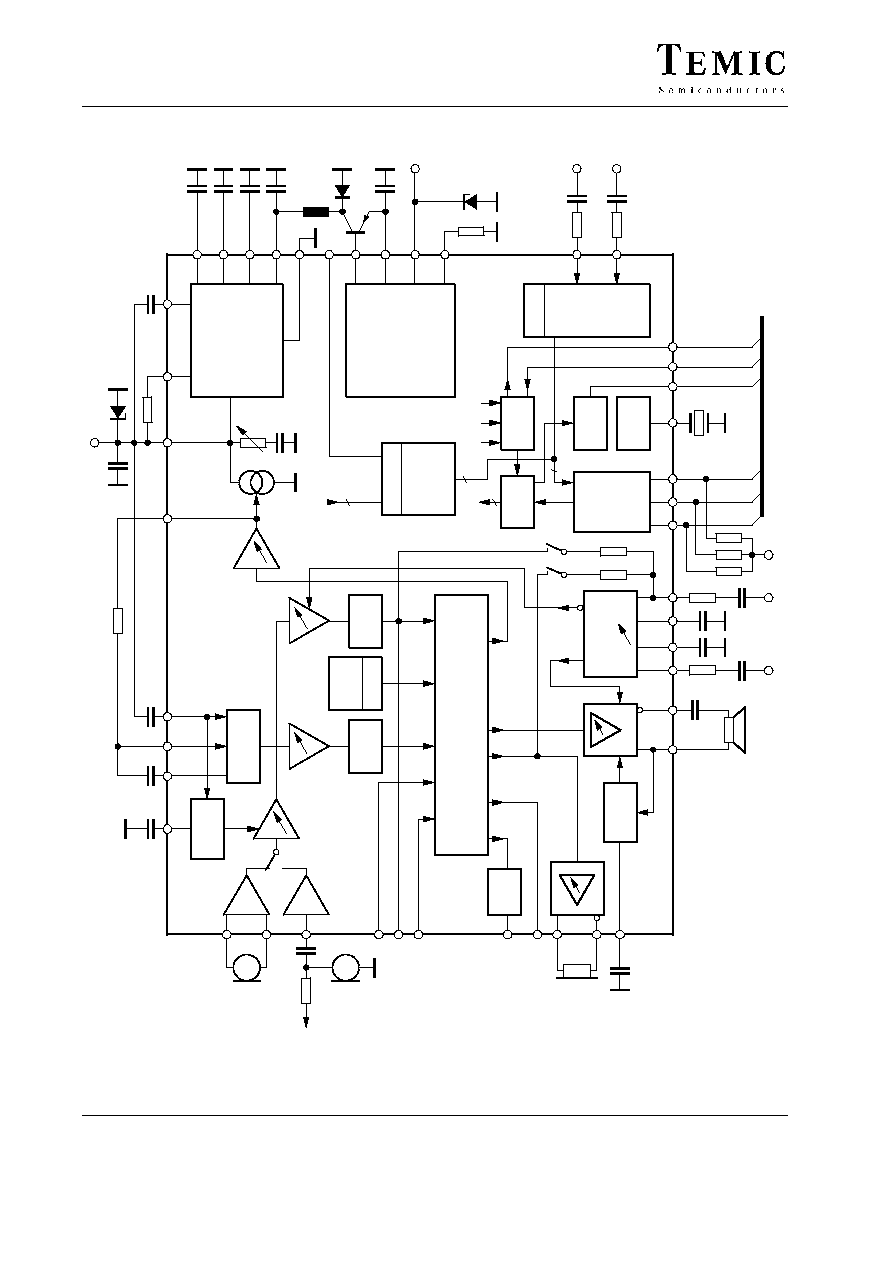
1
Block Diagram
42
43
40
DTMF/
melody
Filter
Offset
canceler
Offset
canceler
CMIC
RXLS
MIC
LRX
DTMF
AMPB
CEAR
AMREC
LTX
EPO
Switch matrix
AGC
AGARX
STBAL
TXACL
39
25
26
10
AGATX
8
41
6
18
4
17
16
14
15
30
31
37
38
44
SACL
1
2
AFS
control
BIDIR
serial
bus
1/8/16/32
DIV.
35 36
33
34
20
21
19
22
23 5
24
3
11
3.58 MHz
OSC.
MUX
ADC
REG
POR
Power
supply
Ringing
power
converter
7
9
V
L
V
RING
V
MIC
14604
RECO1
TXOUT
RA
SA
VMP RFDO
LIDET
TXA
MICRO
mC
V
MP
29
32
28
Filters
CLID
13
12
TIP
RING
27
Figure
2. Block diagram

U3900BM
Target Specification
Rev. A2, 25-Aug-98
5 (34)
2
Class Function
The U3900BM includes a class function Calling Line
IDentification (CLID) for on-hook and Spontaneous Call
Waiting IDentifier (SCWID) for off-hook status.
2.1
CLID
CLID is designed to demodulate CCITT V23 and BELL
202 (1200 bauds FSK asynchronous data) and is
compatible with both formats without external
intervention. It fulfils the CS B14-10W requirements.
The main feature of this part is to provide, for the user,
information about the caller before answering the call.
The information is a DATA message sent from the Central
Office (CO) to the CPE during the silent interval, and
after the first ringing burst.
2.1.1
Description
On the receive side, the received signal coming from
CLI1 and CLI2 first goes to an antialiasing filter after the
differential op-amp.
The next section is a bandpass filter composed of an FSK
filter composed of a fifth order high-pass followed by a
third order low-pass filter. The low-pass and high-pass
cut-off frequencies are about 300 Hz and 3400 Hz
respectively.
2.1.2
Carrier Detect
The carrier detect provides an indication (to the micro-
processor with an interrupt request) of the presence of a
signal in the FSK band. It detects a sufficient amplitude
signal at the output of the FSK bandpass filter.
Note that signals such as speech or DTMF tones also lie
in the FSK frequency band and the carrier detect may be
activated by these signals. The signals will be
demodulated and presented as DATA. To avoid false
DATA detection, a command bit is used to disable the
demodulator when no FSK signal is expected.
Four bits are provided to improve carrier detection
[CD_CD
<3..0
>]. With these bits it is possible to select
a capture window (see the tables next page), and avoid a
false detection.
With the use of SCD bit the carrier detect function is
improved, because after a normal carrier detection
(NCD), a part (10 bits) of the channel seizure is taken in
count before alerting the microprocessor.
Note:
When the CPE is off hook (SCWID mode) the CO sends
FSK data without channel seizure. The
mark signal = 80 bits
±
10 at 1200 bauds (1300 Hz con-
tinuously during 67 ms).
For this case a selected bandpass 1000 Hz to 1700 Hz
could be very useful for the carrier detect ...
After the interrupt due to the carrier detect the micro-
processor can change the bandpass frequencies according
to the FSK band.
D The normal carrier detect guard time is 26.4 ms.
D The improved carrier detect guard time is 34.7 ms.
D The carrier lost guard time is 8.8 ms, in all the cases.
2.1.3
Demodulator
This part is enabled with the carrier detect signal.
The reference signal is at 1700 Hz, (the same frequency
for BELL 202 and V23). All the incoming signals are
compared to this value to make a digital square wave
frequency varying in frequency and in phase as a function
of the input frequencies.
2.1.4
Clock Recovery
The process starts at the first low-level bit received from
the demodulator. After that the CLOCK is generated for
the 10 serial bits (1 bit start, 8 bits data, 1 bit stop).When
all the data are received DATA READY is generated. This
signal loads the serial data in a parallel buffer.
DATA READY provides an indication (to the micro-
processor with an interrupt request) of the presence data
byte available.