
U4037B
Preliminary Information
TELEFUNKEN Semiconductors
Rev. A1, 08-Oct-96
1 (6)
Low Voltage Speech Circuit with Tone Ringer Interface
Description
TELEFUNKEN microelectronic's low voltage speech
and ringer interface circuit, U4037B performs all neces-
sary speech, line interface functions and the tone ringer
required in an electronic telephone set.
The circuit is line powered and contains all components
necessary for amplification of signals and adaption to the
line. The power supply of U4037B provides the MCU
during the ringing and the speech mode.
Features
Speech Circuit
D Adjustable dc characteristic
D Symmetrical input of microphone amplifier
D Receiving amplifier for dynamic or piezo-electric
earpieces
D Automatic line loss compensation
D MCU controlled earphone gain 8 dB
D Anti-clipping in transmit direction
Tone Ringer Interface
D Adjustable volume via 2 bit D/A converter
D Adjustable threshold
D MCU power supply
Benefits
D Low number of external components
Applications
Standard, telephones, fax machines
U4037B
TELEFUNKEN Semiconductors
Rev. A1, 08-Oct-96
Preliminary Information
2 (6)
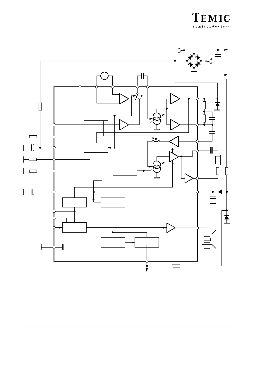
Block Diagram / Applications
Microphone
amplifier
MIC2
MICO
�
+
MIC1
TIN
Transmit
amplifier
Sidetone
amplifier
Supply current
regulator
Control
function
Receiver
attenuation
Receiving
amplifier
Mute control
VL
ST
RECIN
AGC current
generator
RECO1
AGC
VI
VB
Ringer volume
control
Supply
Comparator
with hysteresis
Bandgap
reference
OUT
Tip
Ring
620
W
22
mF
VDD
MELI
VOL2
VOL1
MUTE
DTMF
Receive volume
control
RFO
9879
SWAMP
RDC
GND
RECO2
to
mC
Figure 1. Block diagram

U4037B
Preliminary Information
TELEFUNKEN Semiconductors
Rev. A1, 08-Oct-96
3 (6)
Pin Description
Pin
Symbol
Function
OUT
Buzzer output
MELI
Melody input
RECO1
RECO2
Output of the receiver amplifier
Suitable for dynamic or piezoelec-
tronic transducers
GND
Ground
ST
The output of the sidetone can-
cellation signal, which requires a
balanced impedance of 8 to
10 times the subscribers line
impedance to be connected to
Pin V
L
.
TIN
Input to the line output driver
amplifier, transmit a.g.c. applied
to this stage
MICO
Transmit pre-amplifier output
MIC 1,
MIC 2
Inputs of symmetrical microphone
amplifier with high common mode
rejection ratio
V
DD
Regulated output voltage of for
biasing the MCU
RECIN
Receive amplifier input
The receiving amplification is
regulated by an a.g.c.
V
L
Positive supply voltage input to
the device
The current through this pin is
modulated by the transmit signal.
Pin
Symbol
Function
SWAMP
An external resistor (1 W) is
required from this pin to GND to
control the dc input impedance of
the circuit. It has a nominal value
of 56
W for low voltage operation.
VOI1
VOI2
Volume adjustment of ringer and
earphone amplifier
RFO
Output for ringing frequency
detection
V
I
This internal voltage bias line
must be connected to V
L
via an
external resistor, R
B
, which domi-
nates the ac input impedance of
the circuit and should be 620
for an 600
W input impedance or
910
for a 900
input
impedance.
R
AGC
The range of transmit and receive
gain variations between short and
long loops may be adjusted by
connecting a resistor R
AGC
from
this pin to (GND). This pin can be
left open to set a.g.c. out of action.
DTMF
DTMF input
MUTE
Control input for DTMF operation
VB
Ringer supply
RDC
Input for setting the DC
characteristic
U4037B
TELEFUNKEN Semiconductors
Rev. A1, 08-Oct-96
Preliminary Information
4 (6)
Electrical Characteristics speech circuit
Reference point Pin GND, f = 1000 Hz, 0 dBm = 775 mV
rms,
R
DC
= 60 k
, T
amb
= 25
�
C, unless otherwise specified
Parameters
Test Conditions / Pin
Symbol
Min
Typ
Max
Unit
Line voltage
I
L
= 8 mA
I
L
= 20 mA
I
L
= 30 mA
I
L
= 73 mA
V
L
1.8
3.0
3.6
7.7
2.1
3.3
2.6
3.6
4.5
9.7
V
V
V
V
Transmit and sidetone
Input resistance
R
i
R
i
30
50
75
k
Gain
I
L
= 30 mA
G
s
47
48
49
dB
Line loss compensation
R
AGC
= 0
W, I
L
= 73 mA
DG
s
� 5
�6
� 7
dB
Distortion at line
I
L
> 15 mA, V
L
= 775 mVrms
d
s
2
%
Maximum output voltage
I
L
> 19 mA, d < 5 %,
V
mic
= 10 mV, RDC = 100 k
W
V
1max
1.8
3
4.2
dBm
Anti-clipping attack time
V
mic
= 20 mV, C = 470 nF
0.5
ms
Release time
Each 3 dB overdrive
9
ms
Noise at line weighted
psophometrically
I
L
> 30 mA, G
S
= 48 dB
n
o
� 72
dBmp
Sidetone reduction
I
L
y 20 mA
G
STA
10
15
20
dB
DTMF-amplifier
Volume range d
y 5%
V
0
1
V
RMS
Receiving amplifier
Gain
IL
w 20 mA
G
R
4
dB
Amplification of DTMF signal
from DTMF IN to RECO1/2
I
F
w 15 mA, mute active
G
RM
�15
�12
�9
dB
Frequency response
I
L
> 15 mA, C
L
= 4.7 nF,
f =300 to 3400 Hz
DG
RF
"0.5
dB
Gain change with current
I
L
= 15 to 100 mA
D
GR
"0.5
dB
Gain deviation
T
amb
= �10 to +60
�
C,
I
L
= 15 mA
D
GR
"0.5
dB
Ear protection differential
I
L
w 15 mA, V
gen
= 11 V
rms
2.2
V
rms
Line loss compensation
I
L
= 73 mA
DG
R
� 5
� 6
� 7
dB
Receiving noise at earphone
psophometrially weighted
I
L
= 73 mA
n
i
� 80
� 71
dBm
Gain change when muted
I
L
y 20 mA
G
RM
40
dB
Output voltage push pull
I
L
y 20 mA
V
0
0.8
0.9
1
V
rms
Supply voltage
Output voltage
I
L
y 20 mA
speech mode
V
DDS
3
V
V
Mute suppression
I
L
w 20 mA
G
SM
60
dB

U4037B
Preliminary Information
TELEFUNKEN Semiconductors
Rev. A1, 08-Oct-96
5 (6)
Electrical Characteristics of Tone Ringer Interface
Parameters
Test Conditions / Pin
Symbol
Min
Typ
Max
Unit
Supply current,
outputs open
V
RING
= 14 V
I
S
1.5
2.0
2.5
mA
Switch-on threshold
11
V
Switch-off threshold
6.5
V
Volume adjustment range
VOI1
VOI2
40
dB(A)
Supply voltage for MCU
I
DD
< 1 mA
3.2
V
Ordering Information
Type
Package
U4037B
SO24
Package Information
Package SO24
technical drawings
according to DIN
specifications
1.27
13.97
15.5
15.3
0.49
0.35
2.7
2.45
2.45
2.25
0.3
0.2
0.1 min
10.55
10.15
7.5
7.3
9.25
8.75
Dimensions in mm
95 11492