 | –≠–ª–µ–∫—Ç—Ä–æ–Ω–Ω—ã–π –∫–æ–º–ø–æ–Ω–µ–Ω—Ç: U4055B1 | –°–∫–∞—á–∞—Ç—å:  PDF PDF  ZIP ZIP |

U4055B/U4055B1
Preliminary Information
TELEFUNKEN Semiconductors
Rev. A1, 06-May-96
1 (10)
Low-Voltage Electronic Speech Circuit with Dialer Interface
Description
The U4055B electronic speech circuit is a linear
integrated circuit for use in telephone and other line fed
terminal equipment. It replaces the common speech
circuit with carbon microphone, hybrid transformer,
sidetone equivalent and ear protection rectifiers. A
low-cost electrodynamic transducer is used as the
earphone. It contains all components necessary for
amplification of signals and adaption to the line.
Features
D An electronic circuit replaces the microphone hybrid
transformer
D Symmetrical input for dynamic or piezo microphone
D High performance through the use of dynamic
transducers as the earphone (non-linear distortion
x 2%)
D Automatic line loss compensation
D DTMF interface with muting
D Supply voltage for dialer
D High range of line feeding current
D Input resistance independent of line current and
sidetone suppression circuit.
D Built-in ear protection by earphone voltage limiter
D Operation possible from 8 mA
U4055B1: High level mute; U4055B: Low level mute
Figure 1. Block diagram and pin connection

U4055B/U4055B1
TELEFUNKEN Semiconductors
Rev. A1, 06-May-96
Preliminary Information
2 (10)
Pin Description
Pin
Symbol
Function
1, 2
H
1
and H
2
The push-pull complementary
outputs of the receive amplifier.
Dynamic transducers with a
minimum impedance of 100
W
can be directly driven by these
outputs.
3
GND
Ground.
4
ST
The output of the sidetone
cancellation signal, which
requires a balanced impedance
of 8≠10 times the subscribers
line impedance to be connected
to Pin 13.
5
CK2
Input to the line output driver
amplifier. Transmit a.g.c. applied
to this stage.
6
CK1
The transmit pre-amp output
respective of the DTMF output
which is normally capacitively
coupled to Pin 5.
7, 8
MIC 1,
MIC 2
Inputs of symmetrical
microphone amplifier with high
common mode rejection ratio.
9
DTMF IN The DTMF input has an internal
resistor connected to ground. It
provides the load resistor for the
emitter of a CMOS DTMF
generator. This input is only
active when MUTE (Pin 10) is
pulled high or MUTE is pulled
low.
10
MUTE or
MUTE
The MUTE input must be pulled
at least at 1.5 V (MUTE) or at
less than 0.5 V (MUTE) to mute
the MIC Amp. and Audio Amp.
and enable DTMF IN.
Pin
Symbol
Function
11
V+
Regulated output voltage of
2.7 V for biasing a DTMF
generator activated by MUTE.
12
REC IN
The receive amplifier input. The
receiving amplification is
regulated of an a.g.c.
13
V
L
Positive supply voltage input to
the device. This input should be
connected to the positive output
of the polarity guard. The current
through this pin is modulated by
the transmit signal.
14
R
DC
An external resistor (2 W) is
required from this pin to GND to
control the dc input impedance
of the circuit. It has a nominal
value of 56
W for low voltage
operation. Values up to 100
W
may be used to increase the
available transmit output voltage
swing at the expense of low-
voltage operation.
15
V
I
This internal voltage bias line
must be connected to V
L
via an
external resistor, R
B
, which
dominates the ac input imped-
ance of the circuit and should be
620
for an 600
W input
impedance or 910
for a 900
input impedance.
16
R
AGC
The range of transmit and
receive gain variations between
short and long loops may be
adjusted by connecting a resistor
R
EX1
from this pin to Pin 3
(GND). This pin can be left open
to set a.g.c. out of action.

U4055B/U4055B1
Preliminary Information
TELEFUNKEN Semiconductors
Rev. A1, 06-May-96
3 (10)
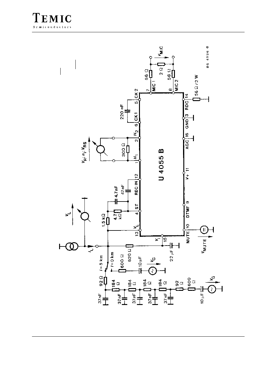
Pin Connection
Figure 2.
Absolute Maximum Ratings
Reference point Pin 3, unless otherwise specified.
Parameters
Symbol
Value
Unit
Line current
I
L
200
mA
DC line voltage, t
p
= 3 ms
Pin 13
V
L
20
V
Power dissipation, I
L
= 100 mA
P
tot
560
mW
Junction temperature
T
j
150
∞
C
Ambient temperature range
T
amb
≠28 to + 80
∞
C
Storage temperature range
T
stg
≠55 to +150
∞
C
Thermal Resistance
Parameters
Symbol
Value
Unit
Junction ambient
R
thJA
85
K/W

U4055B/U4055B1
TELEFUNKEN Semiconductors
Rev. A1, 06-May-96
Preliminary Information
4 (10)
Electrical Characteristics
Reference point Pin 3, cable equivalent = I = 1 km,
0.5 mm, R' = 184
, C' = 37 nF, f = 1300 Hz, 0 dBm = 775 mV
rms,
R
DC
= 56
/ 2 W, T
amb
= 25
∞
C, unless otherwise specified.
Parameters
Test Conditions / Pins
Symbol
Min.
Typ.
Max.
Unit
Line voltage
I
L
= 8 mA
I
L
= 20 mA
I
L
= 30 mA
I
L
= 73 mA, see figure 4
V
L
1.8
3.0
3.6
7.7
2.1
3.3
2.6
3.6
4.5
9.7
V
V
V
V
Transmit and sidetone
see figure 5
Input resistance
Pin 7 - 8
R
i
7
10
13
k
Gain
I
L
= 30 mA
=
l = 5 km
adjustable with R
AGC
I
L
= 30 to 73 mA
l
= 5
km to
0 km
G
s
DG
s
57
≠7
59
61
≠9
dB
dB
Noise at line weighted
psophometrically
I
L
= 73 mA
l
= 0
km
V
MIC
= 0 V
n
o
≠70
≠68
dBm
Sidetone reduction
I
L
y 20 mA
G
STA
10
15
20
dB
DTMF-Amplifier
see figure 6
Input resistance
Pin 8 - 3
R
D
8
10
13
k
DTMF Gain
I
L
= 30 mA
I = 5 km
R
ex1
= 0 adjustable with R
ex1
I
L
= 31 mA to 78 mA = l =
5 km to 0 km
G
D
DG
D
9
≠7
13
≠9
dB
dB
Volume range d
y 5%
V
0
1
V
RMS
Receiving amplifier
see figure 4
Input resistance
Pin 12 - 3
R
i
50
k
Gain
R
HH
= 300
,
I
L
= 30 mA
l =
5 km
R
HH
= 300
adjustable with
R
AGC,
I
L
= 31 mA to 78 mA
l = 5 km to 0 km
G
R
DG
R
≠1
≠5
≠3
≠6
≠5
≠7
dB
dB
Receiving noise at earphone
weighted psophometrially
I
L
= 78 mA = l = 0 km
S2 = 0
n
i
≠80
≠71
dBm
Gain change when muted
I
L
y 20 mA
G
RM
15
20
24
dB
Output saturation threshold
I
L
y 20 mA
V
0
0.8
1
1.5
V
pp
MUTE or MUTE-input
MUTE-input current
Pin 9 = 0 V
I
M
20
50
80
µ
A
MUTE off input voltage
V
Moff
1.5
V
MUTE on input voltage
V
M on
0.3
V
MUTE-input current
Pin 9 = 1.5 V
I
M
10
20
30
µ
A
MUTE off input voltage
V
M off
0.3
V
MUTE on input voltage
V
M on
1.5
V
Supply voltage
see figure 4
Output voltage
I
L
y 20 mA MUTE or MUTE
switched off
switched on
Pin 10
V+
3
2.5
2.9
6.1
3.1
V
V
Output current
I
L
y 20 mA MUTE or MUTE
switched off
switched on
Pin 10
I+
1
30
µ
A
mA
U4055B/U4055B1
Preliminary Information
TELEFUNKEN Semiconductors
Rev. A1, 06-May-96
5 (10)
V
: Receiving voltage when muted
G : Receiving gain at 0 km
G = 20 lg
G = 20 lg
R
V
R
L
RM
R
V
RM
D
V
RM
R
V
Figure 3. Receiving amplifier