
U4065B
Rev. A3, 15-Oct-98
1 (23)
FM Receiver
Description
The IC U4065B is a bipolar integrated FM-frontend
circuit. It contains a mixer, an oscillator, two IF
preamplifiers and an unique interference sensor. The
device is designed for high performance car radio and
home receiver applications.
Features
D All frontend functions of a high performance FM-
receiver, except the RF preamplifier, are integrated
D Improved dynamic range by high current double
balanced mixer design and a new AGC conception
with 3 loops on chip
D Improved blocking and intermod behavior by use of
an unique "interference" sensor controlling the AGC
D Easy cascading of three IF filters (ceramic) by use of
two on-chip IF preamplifiers
D On-chip control functions are available for system
gain adjust (dB linear vs. dc current)
D Low noise LO design
D ESD protected
Block Diagram
V
S
22
1
11
9
8
10
6
17
13
3
5
7
4
21
18
19
16
15
14
23
24
+
IF BPF
IF BPF
IF BPF
IF outp
IF 2
IF 1
IF gain adjust
V
S
Voltage
reg.
IF BPF
ANT
Inter-
ference
mixer
Mixer
RF
PIN
ATT
RF tank
V
tune
RF tank
Local
oscill.
IF tank
LO output
V
ref
= 4 V
20
2
LO tank
AGC adjust
AGC level
V
S
V
S
12
D.N.C.
AGC
(wide band)
wide band
& IF
I F &
detector
Interference
94 8768
U4065B
Rev. A3, 15-Oct-98
2 (23)
Pin Description
Pin
Symbol
Function
1
LOBUFF
Buffered local oscillator output
2
GND1
Ground of the second IF ampli-
fier
3
IF2OUT
Output of the second IF ampli-
fier
4
GAINIF1
Gain control of the first
IF amplifier
5
IF2IN
Input of the second IF amplifier
6
VS
Supply voltage
7
IF1OUT
Output of the first IF amplifier
8
GND2
Ground
9
IMIFIN
Input of the amplifier for the
IM-sensor
10
AGCOUT
Output of the automatic gain
control
11
IMMIXOUT Output of the intermodulation
mixer
12
D.N.C.
Do not connect
Pin
Symbol
Function
13
AGCWB
Threshold adjustment of the
wideband AGC
14
GND3
Mixer ground
15
MIXIN1
Input 1 of the double balanced
mixer
16
MIXIN2
Input 2 of the double balanced
mixer
17
VREF
Reference voltage output
18
MIXOUT1
Mixer output 1
19
MIXOUT2
Mixer output 2
20
GND4
Ground of the first
IF amplifier
21
IF1IN
Input of the first amplifier
22
GND5
Oscillator ground
23
LOE
Local oscillator (emitter)
24
LOB
Local oscillator (base)
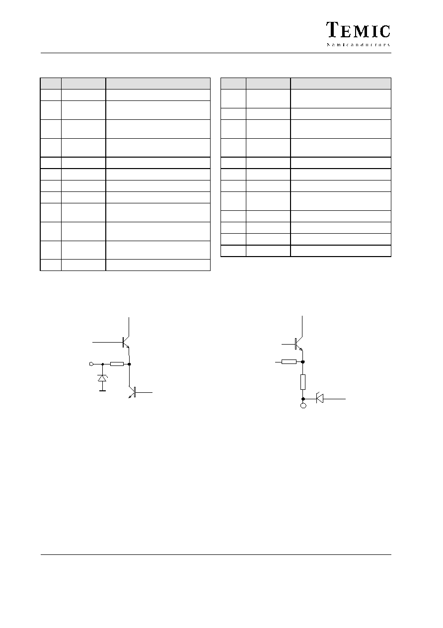
LOBUFF
23
50
1
1 V
ESD
+
94 8769
Buffered local oscillator output:
It drives the FM-input of the PLL circuit (for example
U428xBM-family). The typical parallel output resistance
at 100 MHz is 70
W, the parallel output capacitance is
about 10 pF. When using an external load of 500
W /
10 pF, the oscillator swing is about 100 mV. The second
harmonic of the oscillator frequency is less than
� 15 dBc.
GND1
ESD
2
8
94 8770
Ground of the second IF amplifier:
There is no internal connection to the other ground pins.

U4065B
Rev. A3, 15-Oct-98
3 (23)
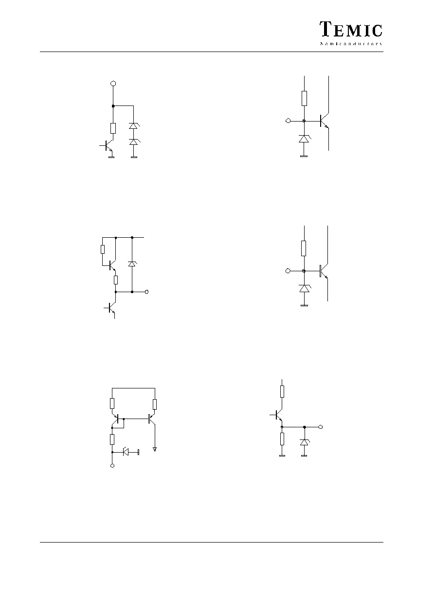
IF2OUT
3
ESD
V
S
V
ref
94 8771
Output of the second IF amplifier:
The parallel output capacitance to ground is about 7 pF.
The external load resistance is to connect to V
S
. The dc
current into the pin is typically 3 mA.
Note: Supply voltage V
S
has to be protected against
IF-distortion
GAINIF1
17
4
ESD
V
ref
2 k
W
94 8772
Gain control of the first IF amplifier:
The gain of the first IF amplifier can be adjusted by a re-
sistor to ground. This is useful for example to com-
pensate the insertion loss tolerances of the ceramic BPF's.
Please ensure that the output current of the pin does not
exceed 150
mA in any case. Linear increasing in the cur-
rent out of GAINIF1 effects dB linear increasing of the
gain (0.15 dB/
mA).
I4 = 0
� G= Gmin = 2 dB
I4 = 140
mA � G = Gmax = 22 dB
IF2IN
ESD
5
V
ref
94 8773
Input of the second IF amplifier:
The parallel input resistance is 330
W. The parallel input
capacitance is about 12 pF. No dc current is allowed. To
avoid overload of this stage an internal detector watches
the input level and causes current at the AGCOUT pin.
IF1OUT
ESD
330
7
V
S
94 8774
Output of the first IF amplifier:
The parallel output resistance is 330
W which allows the
use of a standard ceramic BPF. The parallel output capa-
citance is about 7 pF. The dc voltage at the pin is 0.5 V
less than V
S
.
IMIFIN
9
ESD
94 8775
Input of the IF amplifier for the IM-sensor:
The parallel input resistance is 330
W. The amplifier is ex-
tremely sensitive to ac signals. A few hundred
mV of
IF-signal at this pin will cause current at the AGC output.
Therefore pay attention when connecting the standard ce-
ramic filter used between IMOUT and this pin. The
reference point of the filter has to be free of any ac signal.
Please avoid dc current at this pin.
U4065B
Rev. A3, 15-Oct-98
4 (23)
AGCOUT
10
1 k
1 V
ESD
94 8776
Output of the automatic gain control:
The AGC output is an open collector output. The current
of the pin diode is this current multiplied by the current
gain of the external PNP transistor. The dc voltage at the
pin may vary from 2 V to V
S
, therefore you can easily use
this pin as an indicator of the AGC regulation state.
IMMIXOUT
ESD
300
V
S
1 V
11
94 8777
Output of the intermodulation mixer:
The parallel output resistance is 330
W which allows the
use of a standard ceramic BPF without any further match-
ing network. Please ensure that the ground-pin of the filter
is free of ac signals.
AGCWB
25 k
32 k
ESD
13
V
ref
94 8778
Threshold adjustment of the wideband AGC:
The threshold of the wideband AGC can be adjusted by
an external resistor to ground. The setting range is 10 dB.
For minimum blocking this pin is connected to ground. In
order to set the threshold to smaller levels the resistance
value should be up to a few hundred k
W.
MIXIN1
2.5 k
15
ESD
V
ref
94 8779
Input 1 of the double balanced mixer:
The parallel input resistance is 1.2 k
W. The parallel input
capacitance is about 9 pF. When using the mixer unbal-
anced this pin is to be grounded for RF-signals by an
external capacitance of a few nF. DC current is not allowed.
MIXIN2
2.5 k
16
ESD
V
ref
94 8780
Input 2 of the double balanced mixer:
The parallel input resistance is 1.6 k
W. The parallel input
capacitance is about 7 pF. The double sideband noise fig-
ure of the unbalanced mixer is about 7 dB. In the balanced
case the noise figure will be reduced by about 0.8 dB.
VREF
94 8781
4.6 V
200
ESD
V
S
17
Reference voltage:
The internal temperature compensated reference voltage
is 3.9 V. It is used as bias voltage for most blocks, so the
electrical characteristics of the U4065B are widely inde-
pendent of the supply voltage. The internal output
resistance of the reference voltage is less than 10
W. To
avoid internal coupling across this pin external capacitors
are required. The maximum output current is I
ref
= 5 mA.

U4065B
Rev. A3, 15-Oct-98
5 (23)
MIXOUT1, MIXOUT2
18
ESD
94 8782
19
Mixer output 1, 2:
The mixer output is an open collector of a bipolar transis-
tor. The minimum voltage at this pins is 5 V (V
S
-voltage
swing). The dc current into this pins is typically 9 mA.
Good LO- and RF suppression at the mixer output can be
achieved by symmetrical load conditions at the pins MIX-
OUT1 and MIXOUT2.
IF1IN
21
330
V
ref
ESD
94 8784
Input of the first IF amplifier:
The typical input resistance is 330
W. The dc voltage is
nearly the same one as the reference voltage. Please avoid
dc current at this pin.
LOE
23
ESD
94 8785
Emitter of the local oscillator:
An external capacitor is connected between LOE and
ground. The ground pin of this capacitor is to connect to
the pin GND5. GND5 is the chip internal ground of the
local oscillator.
LOB
24
ESD
94 8786
Base of the local oscillator:
The tank of the local oscillator is connected at pin LOB.
The ground pin of this tank is to connect to the pin GND5.
GND5 is the chip internal ground into pin 24 of the local
oscillator. The resonant resistance of the tank should be
about 250
W. Minimum Q of the unloaded tank is 50.