U4084B
Preliminary Information
TELEFUNKEN Semiconductors
Rev. A1, 31-Jan-97
1 (26)
Low-Voltage, Voice-Switched Circuit for Hands-Free Operation
Description
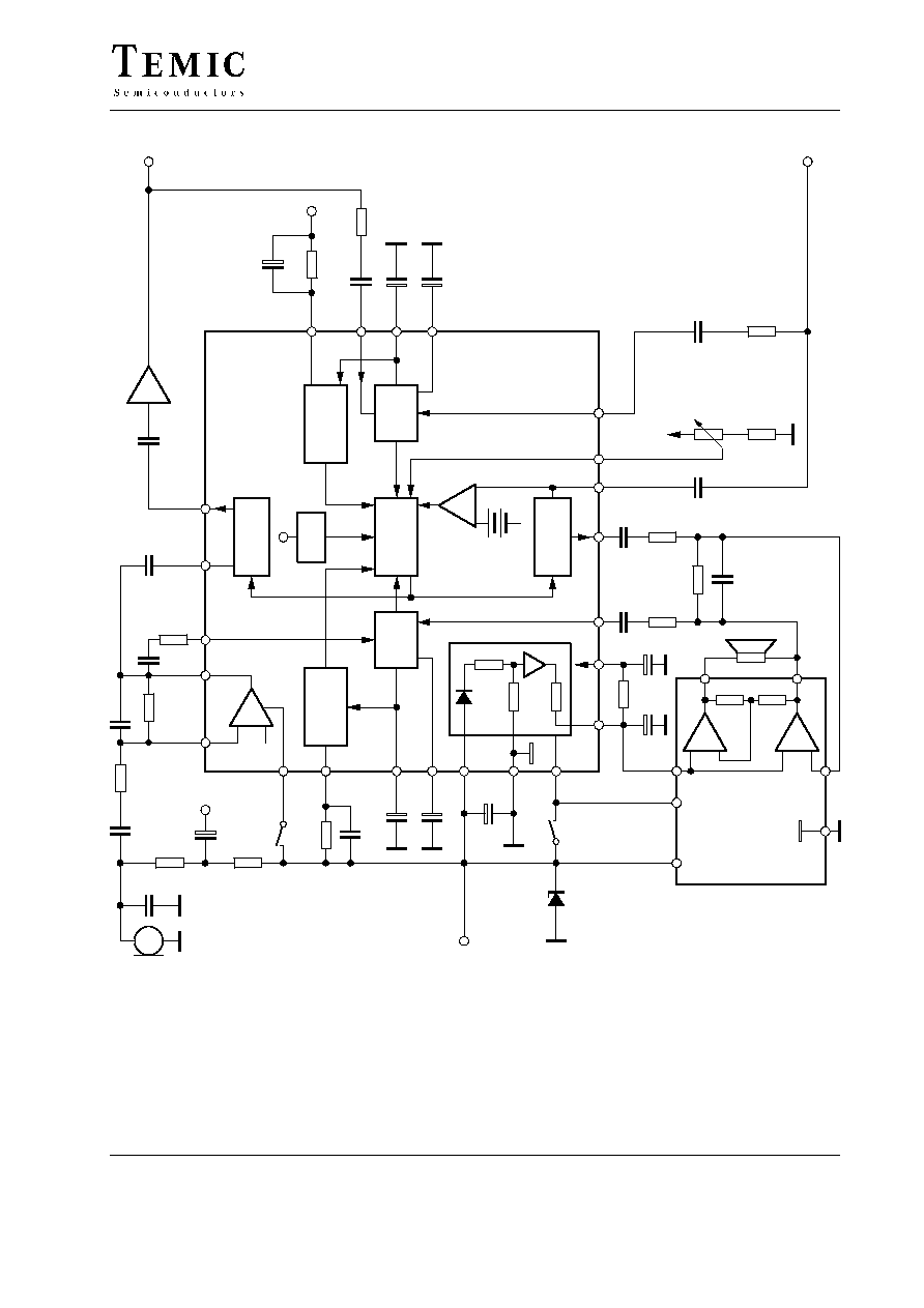
The low-voltage, voice-switched speakerphone circuit
U4084B incorporates the features listed below. The ver-
satility of the device is further enhanced by giving access
to internal circuit points.
The block diagram shows amplifiers, level detectors,
transmit and receive attenuators operating in comple-
mentary functions, back ground noise monitors, chip
disable, dial tone detector and mute function etc.
Due to low-voltage operation, it can be operated either by
low supply voltage or via a telephone line requiring
4.0 mA typ. Further features are stand-alone operation
via a coupling transformer (Tip and Ring) or in
conjunction with a handset speech network, as shown in
figure 2.
Features
D Low-voltage operation: 3.0 to 6.5 V
D Attenuator gain range between
transmit and receive: 52 dB
D Four-point signal sensing for improved sensitivity
D Monitoring system for background-noise level
D Microphone-amplifier gain adjustable
D Mute function
D Chip disable for active/ standby operation
D Dial tone detector
D Compatible with the speaker amplifier U4083B
D Case: DIP24 or SO24
Benefits
D Fast channel switching enables quasi duplex
operation
D Low current consumption for high output volume
D Optimized U3800BM interface

U4084B
TELEFUNKEN Semiconductors
Rev. A1, 31-Jan-97
Preliminary Information
4 (26)
Pin Description
Pin
Symbol
Function
1
GND
Ground
2
NC
Not connected
3
CD
Chip disable.
A logic LOW (< 0.8 V) sets normal
operation. A logic HIGH (> 2.0 V)
disables the IC to conserve power.
The input impedance is nominally
90 k
W.
4
V
S
Supply voltage 2.8 to 6.5 V,
approximately @ 4 mA.
The AGC circuit reduces the receive
attenuator gain @ 25 dB.
Receive mode @ 2.8 V.
5
TO
Transmit attenuator output.
The DC level is approximately V
B
.
6
TI
Transmit attenuator input.
Max. signal level is 350 mV
rms
.
The input impedance is approxi-
mately 10 k
W.
7
MICO
Microphone amplifier output.
The gain is set by external resistors.
8
MIC
Microphone amplifier input.
The bias voltage is approximately
V
B
.
9
MUTE
Mute input.
A logic LOW (< 0.8 V) sets normal
operation. A logic HIGH (> 2.0 V)
mutes the microphone amplifier
without affecting the rest of the
circuit. The input impedance is
nominally 90 k
W.
10
VCI
Volume control input.
When VCI = V
B
, the receive attenu-
ator is at maximum gain in the
receive mode.
When VCI = 0.3 V
B
, the receive
gain is 35 dB lower. This does not
affect the transmit mode.
Pin
Symbol
Function
11
C
T
Response time.
An RC at this pin sets the response
time for the circuit to switch modes.
12
V
B
Output voltage
V
S/2
.
It is a system AC ground, and biases
the volume control. A filter cap is
required.
13
CPT
An RC at this pin sets the time
constant for the transmit background
monitor.
14
TLI2
Transmit-level detector input on the
microphone/ speaker side.
15
TLO2
Transmit-level detector output on
the microphone/ speaker side, and
input to the transmit background
monitor.
16
RLO2
Receive-level detector output on the
microphone/ speaker side
17
RLI2
Receive-level detector input on the
microphone/ speaker side
18
RI
Input receive attenuator and dial-
tone detector.
The max. input level is 350 mV
rms
.
The input impedance is approxi-
mately 10 k
W.
19
RECO
Receive attenuator output.
DC level is approximately V
B
.
20
TLI1
Transmit-level detector input on the
line side
21
TLO1
Transmit-level detector output on
the line side
22
RLO1
Receive-level detector output on the
line side, and input to the receive
background monitor
23
RLI1
Receive-level detector input on the
line side
24
CPR
An RC at this pin sets the time
constant for the receive background
monitor

U4084B
Preliminary Information
TELEFUNKEN Semiconductors
Rev. A1, 31-Jan-97
5 (26)
Absolute Maximum Ratings
Reference point Pin 1, T
amb
= 25
∞
C, unless otherwise specified.
Parameters
Symbol
Value
Unit
Supply voltage
Pin 4
V
S
≠1.0 to +7.0
V
Voltages
Pins 3 and 9
Pin 10
Pins 6 and 18
≠1.0 to (V
S
+ 1.0)
≠1.0 to (V
S
+ 0.5)
≠0.5 to (V
S
+ 0.5)
V
Storage temperature range
T
stg
≠55 to +150
∞
C
Junction temperature
T
j
125
∞
C
Ambient temperature range
T
amb
≠20 to +60
∞
C
Power dissipation
T
amb
= 60
∞
C
DIP24
SO24
P
tot
P
tot
650
520
mW
Maximum Thermal Resistance
Parameters
Symbol
Value
Unit
Junction ambient
DIP24
SO24
R
thJA
R
thJA
100
120
K/W
K/W
Operation Recommendation
Parameters
Test Conditions / Pins
Symbol
Min.
Typ.
Max.
Unit
Supply voltage
Pin 4
V
S
3.5
≠
6.5
V
CD input
MUTE input
Pin3
Pin 9
0
≠
V
S
V
Output current
Pin 12
I
B
≠
≠
500
mA
Volume control input
Pin 10
VCI
0.3
V
B
≠
V
B
V
Attenuator input signal
voltage
Pins 6 and 18
0
≠
350
mV
rms
Microphone amplifier
0
≠
40
dB
Load current
@ RECO, TO Pins 5, 19
@ MICO
Pin 7
0
0
≠
≠
"2.0
"1.0
mA
Ambient temperature range
T
amb
≠20
≠
+60
∞
C