U4087B
Preliminary Information
TELEFUNKEN Semiconductors
Rev. A1, 09-Sep-96
1 (8)
Low Voltage Voice Switch Interface Circuit for Hands-free
Operation in Telephone
Description
The voice switch interface circuit U4087B is a linear
integrated circuit for improvement of handsfree
performance of U4090B system.
The U4087B provides an optimized interface to U4090B,
the necessary level detectors and switching control for a
properly operating speakerphone. The detection
sensitivity and timing are externally controllable.
Additionally, the U4087B provides a back- ground noise
monitor which makes the circuit insensitive to room
noise.
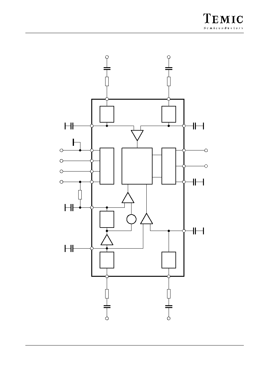
The Block diagram shows level detectors, back ground
noise monitor.
Due to low voltage operation it can be operated via power
supply management of U4090B requiring 1.0 mA typ.
Features
D Low voltage operation: 3.0 to 7.0 V
D Four point signal sensing
D Monitoring system for background noise level
D Case: SO 16
D Chip Disable for active/standby operation
Benefits
D Fast channel switching allows quasi duplex operation
D Low current consumption
Block Diagram
Bias
Noise
detector
7
13
6
5
TS
≠
+
=
14
+
≠
Logic
15
Logic
16
C.T.
Generator
Charge
DIRA
Discharge
Logic
9
≠
+
DIRE
2
Logic
Logic
1
4
10
11
12
CT
8
12610
TLO2
CPT
VB
VM
CD GND
TLO1
TLI1
RLI1
3
TLDR
TLDT
RLO1
RLO2
RLI2
TLI2
Figure 1. Block diagram with external circuit

U4087B
Preliminary Information
TELEFUNKEN Semiconductors
Rev. A1, 09-Sep-96
5 (8)
Pin Description
Pin
Symbol
Function
1
TLI1
Transmit level detector input on the line side
2
TLO1
Transmit level detector output on the line side
3
RLO1
Receive level detector output on the line side
4
RLI1
Receive level detector input on the line side
5
GND
Ground
6
CD
Chip Disable
A logic low (< 0.8 V) sets normal operation. A logic high (> 2.0 V) disables the IC to con-
serve power. Input impedance is nominally 90 k
W.
7
V
B
Supply voltage 2.8 to 7.0 V, approx. @ 1 mA
8
RLO2
Receive level detector output on the microphone/speaker side
9
RLI2
Receive level detector input on the microphone/speaker side
10
TLDR
Positive control output for U4090B
11
TLDT
Negative control output for U4090B
12
C
T
Response time
An RC at this pin sets the response time for the circuit to switch modes
13
V
M
It is a system ac ground, supplied by U4090B, V
M
X VB/2
14
CPT
An RC at this pin sets the time constant for the transmit background monitor
15
TLI2
Transmit level detector input on the microphone/speaker side
16
TLO2
Transmit level detector output on the microphone/speaker side, and input to the transmit
background monitor
Absolute Maximum Ratings
Reference point Pin 1, T
amb
= 25
∞
C, unless otherwise specified
Parameters
Symbol
Value
Unit
Supply voltage
Pin 7
V
B
≠ 0.3 to + 12
V
Voltages:
Pin 6
Pin 13
≠ 0.3 to 6
≠ 0.3 to (V
B
+ 0.3)
V
Storage temperature range
T
stg
≠ 55 to + 150
∞
C
Junction temperature
T
j
125
∞
C
Ambient temperature range
T
amb
≠ 20 to + 60
∞
C
Power dissipation
T
amb
= 60
∞
C
SO 16
P
tot
750
mW
Maximum thermal resistance
Junction ambient
SO 16
R
thJA
110
K/W
Operation Recommendation
Parameters
Test conditions / Pin
Symbol
Min.
Typ.
Max.
Unit
Supply voltage
Pin 7
V
B
3.0
≠
7.0
V
CD input Pin 6
0
≠
V
B
V
Ambient temperature range
T
amb
≠ 20
≠
+ 60
∞
C