TELEFUNKEN Semiconductors
U4091B
Preliminary Information
Rev. A1: 12.07.1995
1 (11)
Programmable Telephone Audio Processor
Description
The programmable telephone audio processor U4091B is
a linear integrated circuit for use in feature phones, an-
swering machines and fax machines. It contains the
speech circuit, tone ringer interface with dc/dc converter,
sidetone equivalent and ear protection rectifiers. The cir-
cuit is line powered and contains all components
necessary for amplification of signals and adaptation to
the line.
An integrated voice switch with loudspeaker amplifier al-
lows handsfree or loudhearing operation. With an
anti-feedback function, acoustical feedback during loud-
hearing can be reduced significantly. The generated
supply voltage is suitable for a wide range of peripheral
circuits.
Features
D Speech circuit with anti-clipping
D Tone ringer interface with dc / dc converter
D Speaker amplifier with anti-distortion
D Power supply management, regulated, unregulated
and a special supply for electret microphone
D Voice switch
Benefits
D Savings of one piezo electric transducer
D Complete system integration of analog signal proces-
sing on one chip
D Very few external components
Applications
Feature phone, answering machine, fax machine, speaker
phone
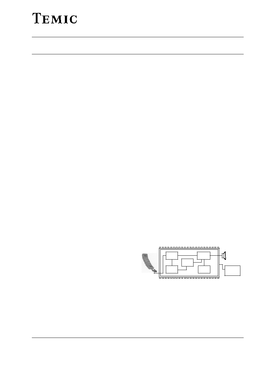
MC with
EEPROM/
DTMF
Audio
amplifier
Speech
circuit
Voice
switch
Tone
ringer
Loudhearing
and
Tone ringing
¡¡
¡¡
BUS

TELEFUNKEN Semiconductors
U4091B
Preliminary Information
Rev. A1: 12.07.1995
2 (11)
Serial Bus Controlled Functions
Speech circuit
D Transmit gain: 36 to 52 dB (1 dB step)
D Receive gain: ≠7 dB to +9 dB (1 dB step) + one 6 dB
step
D Speaker amplifier gain: ≠10 dB to +30 dB (1.5 dB
step)
D Mute R, Mute T
D Automatic gain adjustment ( AGA ): 7 different
characteristics
D Impedance selection: 600/ 900 W
Ringer
D Volume adjustment
Voice switch
D Volume adjustment
D Attenuation range: 0 to 50 dB (1 dB steps)
D 4 thresholds for mode switching
D Mute of handsfree microphone
D Chip disable
D Hand set / handsfree switching
D Four point level detection

TELEFUNKEN Semiconductors
U4091B
Preliminary Information
Rev. A1: 12.07.1995
3 (11)
Pin Description
Pin
Symbol
Function
DTMF
Input for DTMF signals, also used
for the answering machine and
handsfree input
MICO
Output of microphone preamplifier
MIC 2
Non-inverting input of microphone
amplifier
MIC 1
Inverting input of microphone
amplifier
PD
Active high input for reducing the
current consumption of the circuit,
simultaneously V
L
is shorted by an
internal switch
IND
The internal equivalent inductance
of the circuit is proportional to the
value of the capacitor at this pin, a
resistor connected to ground may be
used to reduce the dc line voltage
V
L
Line voltage
GND
Reference point for dc- and
ac-output signals
SENSE
A small resistor (fixed) connected
from this pin to V
L
sets the slope of
the dc characteristic and also effects
the line length equalization
characteristics and the line current
at which the loudspeaker amplifier
is switched on
V
B
Unregulated supply voltage for
peripheral circuits (voice switch),
limited to typically 7 V
SAO
Output of loudspeaker amplifier
V
MPS
Unregulated supply voltage for
µ
P,
limited to 6.3 V
V
MP
Regulated supply voltage 3.3 V for
peripheral circuits (especially
microprocessors), maximum output
current: 2 mA
SWOUT Output for driving external
switching transistor
COSC
40 kHz oscillator for ringing power
converter
VRING
Input for ringing signal
THA
Threshold adjustment for ringing
frequency detector
RFDO
Output of ringing frequency detector
LIDET
Line detect; output is low when the
line current is more than 15 mA
Pin
Symbol
Function
TSACL
Time constant of anti-clipping of
speaker amplifier
SA I
Speaker amplifier input (for
loudspeaker, tone ringer and
handsfree use)
RLO1
Receive level output 1
RLI1
Receive level input 1
MICHF
Handsfree Mic input
BNMT
Background noise monitor in trans-
mit direction
RLI2
Receive level input 2
RLO2
Receive level output 2
C
Clock
D
Data
Reset
Reset
IREF
Internal reference current
generation; RREF = 62 k
;
IREF = 20
µ
A
STO
Side tone reduction output
output resistance is approx. 300
,
maximum load impedance: 10 k
.
V
M
Reference node for microphone-
earphone and loudspeaker amplifier,
supply for electret microphone
(IM
300
mA)
RECO 2
Inverting output of receiving
amplifier
STI S
Input for side tone network (short
loop) or for answering machine
STI L
Input for side tone network (long
loop)
RAC
Input of receiving amplifier for ac
coupling in feedback path
RECO 1
Output of receiving amplifier
TTXA
Time constant of anticlipping in
transmit path
RECIN
Input of receiving path; input
impedance is typically 80 k
W
TXIN
Input of intermediate transmit stage,
input resistance is typically 20 k
TLDI
Transmit level detector input
TLDO
Time constant of level detector for
transmit voice recognition
TS
Time constant for switching
TELEFUNKEN Semiconductors
U4091B
Preliminary Information
Rev. A1: 12.07.1995
5 (11)
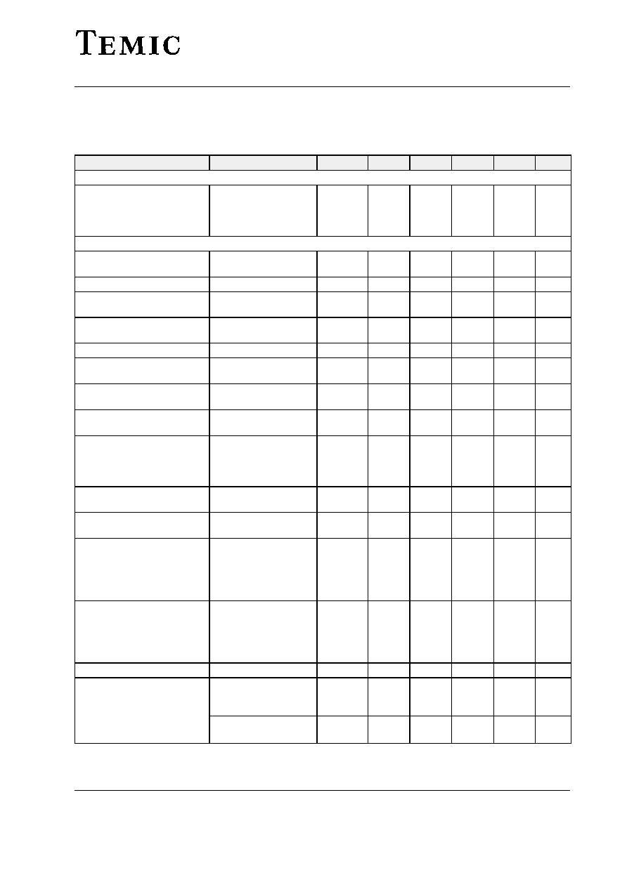
Electrical Characteristics
f = 1 kHz, 0 dBm = 775 mV
rms
, I
M
= 0.3 mA, I
MP
= 2 mA, RDC = 130 k
W, T
amb
= 25
∞
C,
Z
ear
= 68 nF + 100
W, Z
M
= 68 nF, unless otherwise specified.
Parameters
Test Conditions / Pin
Symbol
Min.
Typ.
Max.
Unit
Figure
DC characteristics
DC voltage drop over circuit
I
L
= 2 mA
I
L
= 14 mA
I
L
= 60 mA
I
L
= 100 mA
V
L
4.6
8.8
2.4
5.0
7.5
9.4
5.4
10.0
V
Transmission amplifier, I
L
= 14 mA, V
MIC
= 2 mV, RGT = 27 k
W, unless otherwise specified
Adjustment range of transmit
gain
G
T
36
52
dB
Transmitting amplification
G
T
47
48
49
dB
Frequency response
I
L
w 14 mA,
f = 300 to 3400 Hz
DG
T
"0.5
dB
Gain change with current
Pin 31 open
I
L
= 14 to 100 mA
DG
T
"0.5
dB
Gain deviation
T
amb
= ≠ 10 to + 60
∞
C
DG
T
"0.5
dB
CMRR of microphone
amplifier
CMRR
60
80
dB
Input resistance of MIC
amplifier
RGT = 12 k
W
RGT = 27 k
W
R
i
45
50
75
110
k
W
Distortion at line
I
L
> 14 mA
V
L
= 700 mVrms
d
t
2
%
Maximum output voltage
I
L
> 19 mA
d < 5%
Vmic = 25 mV
CTXA = 1
mF
V
Lmax
1.8
3
4.2
dBm
Noise at line psophomet-
rically weighted
I
L
> 14 mA
G
T
= 48 dB
no
≠ 80
≠72
dBmp
Anti-clipping attack time
release time
CTXA = 1
mF
each 3 dB overdrive
0.5
9
ms
Gain at low operating current
I
L
= 10 mA
I
MP
= 1 mA
RDC = 68 k
W
Vmic = 1 mV
I
M
= 300
mA
G
T
40
42.5
dB
Distortion at low operating
current
I
L
= 10 mA
I
M
= 300
mA
I
MP
= 1 mA
RDC = 68 k
W
Vmic = 10 mV
d
t
5
%
Line loss compensation
I
L
= 100 mA
DG
TI
≠ 6.4
≠ 5.8
≠ 5.2
dB
Mute suppression
a) MIC muted (microphone
preamplifier
I
L
w 14 mA
Mutx = open
G
TM
60
80
dB
p
p
b) TXA muted (second
stage)
IMPSEL = open
G
TTX
60
dB