 | –≠–ª–µ–∫—Ç—Ä–æ–Ω–Ω—ã–π –∫–æ–º–ø–æ–Ω–µ–Ω—Ç: U4254BM | –°–∫–∞—á–∞—Ç—å:  PDF PDF  ZIP ZIP |
U4254BM
TELEFUNKEN Semiconductors
Rev. A1, 08-Jul-97
1 (12)
Low-Noise AM/FM Antenna Impedance Matching IC
Description
The U4254BM is an integrated low-noise AM/FM
antenna impedance matching circuit in BICMOS
technology. The device is designed in particular for car
application and is suitable for windscreen and roof
antennas.
Features
D High dynamic range for AM and FM
D Integrated AGC for FM
D High intercept point 3rd order for FM
D FM amplifier adjustable to various cable impedance
D High intercept point 2nd order for AM
D Low noise output voltage
D Low power consumption
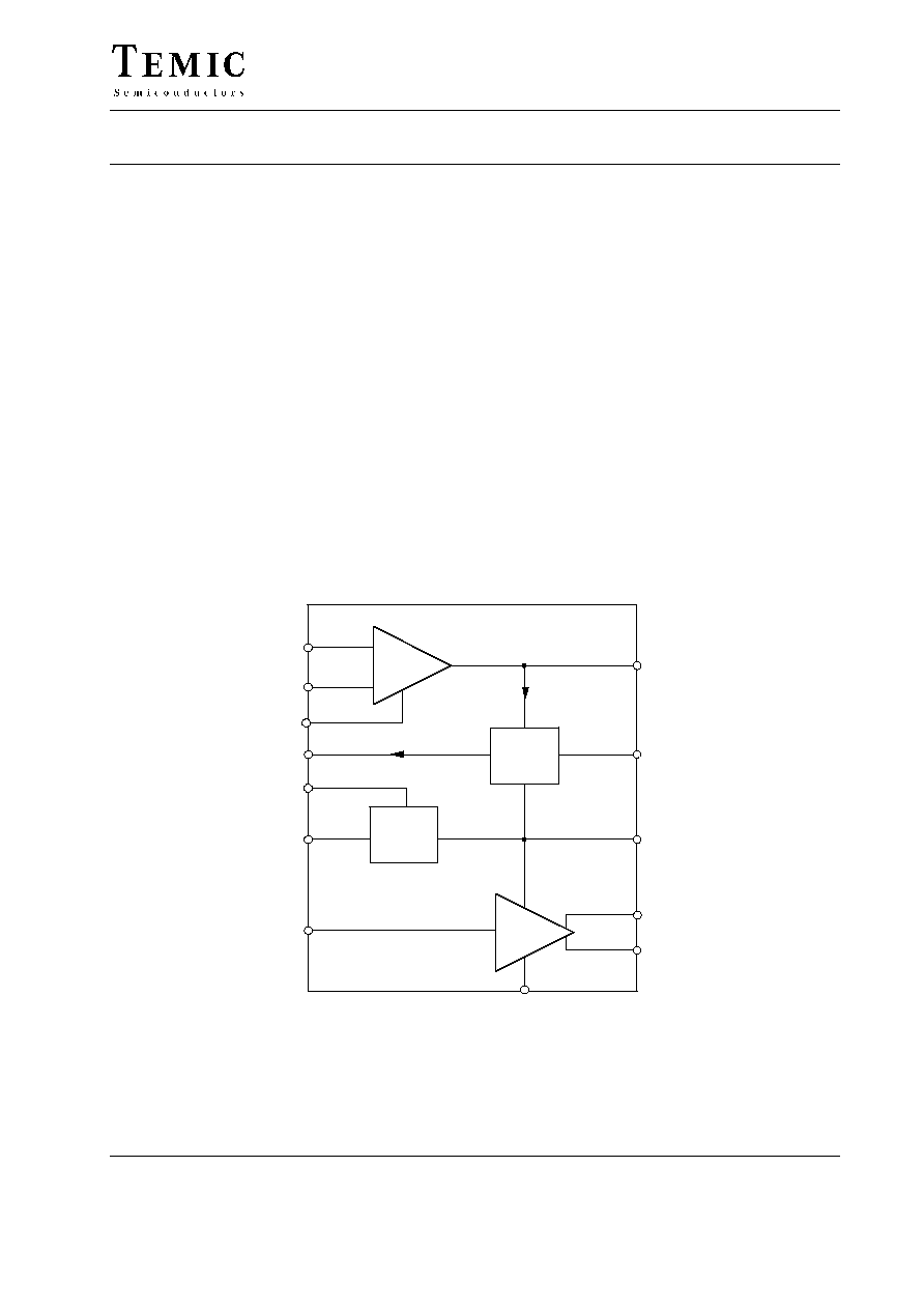
Block Diagram
FM
AGC
FMIN
AGC
VS
AMIN
AMOUT
VREF1
FMOUT
FMGAIN
GND1
I
AGC
AGCADJ
GND2
VREF2
VREF
1
2
4
3
5
7
8
10
14
12
13
15
AMOUT1
11
AM
13932
Figure 1. Block diagram

U4254BM
TELEFUNKEN Semiconductors
Rev. A1, 01-Jul-97
2 (12)
Ordering and Package Information
Extended Type Number
Package
Remarks
U4254BM-AFP
SO16
U4254BM-AFPG3
SO16
Taping corresponding, ICE-286-3
Pin Description
1
2
3
4
5
6
7
8
16
15
14
13
12
11
10
9
FMGAIN
AGC
VREF2
NC
GND2
AMIN
FMIN
GND1
VS
AGCADJ
VREF1
AMOUT1
AMOUT
NC
NC
FMOUT
13933
Figure 2. Pinning
Pin
Symbol
Function
1
FMIN
FM input
2
GND1
Ground for FM part
3
FMGAIN
FM gain adjustment
4
AGC
AGC output
5
VREF2
Reference voltage 2 output
6
NC
Not connected
7
GND2
Ground for AM part
8
AMIN
AM input
9
NC
Not connected
10
AMOUT
AM output
11
AMOUT1 AM output
12
VREF1
Reference voltage 1 output
13
AGCADJ
Adjustment FM wide-band
AGC threshold
14
VS
Supply voltage
15
FMOUT
FM output
16
NC
Not connected
U4254BM
TELEFUNKEN Semiconductors
Rev. A1, 08-Jul-97
3 (12)
Pin Description
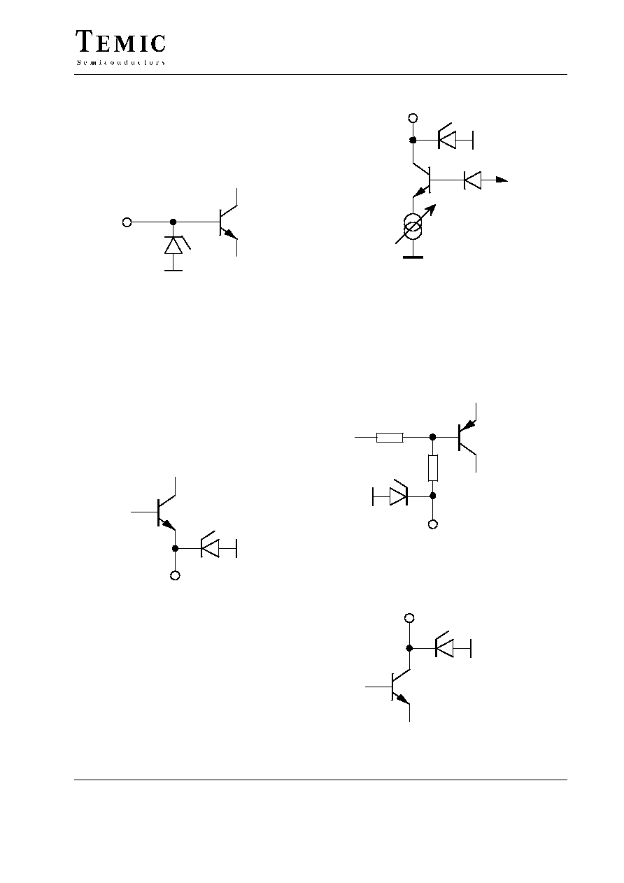
FMIN
FMIN is the input of the FM amplifier. It is the base of a
bipolar transistor. A resistor or a coil is connected
between FMIN and VREF2. If a coil is used, noise perfor-
mance is excellent.
ESD
1
FMIN
12390
Figure 3.
GND1
To avoid crosstalk between AM and FM signals, the
circuit has two separate ground pins. GND1 is the ground
for the FM part.
FMGAIN
The DC current of the FM amplifier transistor is adjusted
by an external resistor which is connected between
FMGAIN and GND1. In order to influence the AC gain
of the amplifier, a resistor is connected in series to an
capacitor between FMGAIN and GND1. The capacitor
has to be a short at frequencies of 100 MHz.
ESD
3
FMGAIN
12391
Figure 4.
AGC
DC current flows into the AGC pin at high FM antenna
input signals. This current has to be amplified via the cur-
rent gain of an external PNP transistor that feeds a
PIN-diode. This diode dampens the antenna input signal
and protects the amplifier input against overload. The
maximum current which flows in the AGC pin is approxi-
mately 1 mA. In low end applications, the AGC function
is not necessary and therefore the external components
can be omitted.
ESD
4
V
S
AGC
12392
Figure 5.
AGCADJ
The threshold of the AGC can be adjusted by variing the
DC current at pin AGCADJ. If pin AGCADJ is connected
directly to GND1, the threshold is set to 96 dB
µ
V at the
FM amplifier output. If a resistor is connected between
AGCADJ and GND1, the threshold is shifted to higher
values with increasing resistances. If AGCADJ is open,
the threshold is set to 106 dB
µ
V.
ESD
13
65 k
W
12397
AGCADJ
Figure 6.
FMOUT
The FM amplifiers output is an open collector of a bipolar
RF-transistor. It should be connected to VS via a coil.
ESD
15
12398
FMOUT
Figure 7.

U4254BM
TELEFUNKEN Semiconductors
Rev. A1, 01-Jul-97
4 (12)
AMIN
The AM input has an internal bias voltage. The DC
voltage at this pin is V
Ref1
/2. The input resistance is about
470 k
W. The input capacitance is less than 10 pF.
ESD
8
470 k
W
VREF1/2
12394
AMIN
Figure 8.
AMOUT, AMOUT1
The buffered AM amplifier consists of a complementary
pair of CMOS source followers. The transistor gates are
connected to AMIN. The pin AMOUT is the NMOS
transistor's source, pin AMOUT1 is the PMOS transistor'
source. Due to the two different DC levels of these pins,
they have to be connected together via an external
capacitor of about 100 nF. By means of this technique an
excellent dynamic range can be achieved.
AMOUT1
ESD
ESD
AMOUT
13768
11
10
Figure 9.
VREF1
VREF1 is the stabilized voltage for the AM amplifier and
the AGC block. To achieve excellent noise performance
at LW frequencies, it is recommended that this pin is
connected to ground via an external capacitor of about
1
mF.
ESD
12
VS
GND1
12396
VREF1
Figure 10.
VREF2
For the DC biasing of the FM amplifier a second voltage
reference circuit is integrated. Because of temperature
independence of the collector current the output voltage
has a negative temperature coefficient of about ≠1 mV/K.
To stabilize this voltage an external capacitor to ground
of a few nF is recommended.
ESD
5
GND1
12393
VREF2
Figure 11.
GND2
GND2 is the ground for the AM amplifier.

U4254BM
TELEFUNKEN Semiconductors
Rev. A1, 08-Jul-97
5 (12)
Functional Description
The U4254BM is an integrated AM/FM antenna imped-
ance matching circuit. It compensates cable losses
between the antenna (for example windscreen, roof or
bumper antennas) and the car radio which is usually
placed far away from the antenna.
The FM amplifier provides excellent noise performance.
External components are used to adjust the gain and the
input-output matching impedance. Therefore it is
possible to adjust the amplifier to various cable
impedances (usually 50, 75 or 150
W). To protect the
amplifier against input overload an Automatic Gain
Control (AGC) is included on the chip. The AGC
observes the AC voltage at the FM amplifier output,
rectifies this signal, and delivers DC current to dampen
the input antenna signal via an external PIN diode. The
threshold for the AGC is adjustable. Simple and
temperature compensated biasing is possible due to the
integrated voltage reference V
Ref2
.
The AM part consists of a buffer amplifier. The voltage
gain of this stage is approximately one. The input
resistance is 470 k
W, the input capacitance less than
10 pF. The output resistance is 125
W. An excellent
dynamic range is achieved due to the complementary
CMOS source follower stage.
Absolute Maximum Ratings
Reference point is ground (Pins 2 and 7)
Parameters
Symbol
Value
Unit
Supply voltage
V
S
8.8
V
Power dissipation, P
tot
at T
amb
= 85
∞
C
P
tot
460
mW
Junction temperature
T
j
150
∞
C
Ambient temperature
T
amb
≠40 to +85
∞
C
Storage temperature
T
stg
≠50 to +150
∞
C
Electrostatic handling (HBM)
"V
ESD
2000
V
Thermal Resistance
Parameters
Symbol
Value
Unit
Junction ambient
R
thJA
140
K/W