 | –≠–ª–µ–∫—Ç—Ä–æ–Ω–Ω—ã–π –∫–æ–º–ø–æ–Ω–µ–Ω—Ç: U4256BM | –°–∫–∞—á–∞—Ç—å:  PDF PDF  ZIP ZIP |
U4256BM
Preliminary Information
Rev. A2, 03-Nov-98
1 (14)
Frequency Synthesizer for Radio Tuning
Description
The U4256BM is a single chip frequency synthesizer in
BICMOS technology. Together with the AM/FM IC
U4255BM, it performs a complete AM/FM car radio front
end, which is recommended also for RDS (Radio Data
System) applications. It is controlled by 3-wire bus and
contains also Digital to Analog Converters (DACs) for
automatic alignment of the AM/FM tuner.
Features
D Reference oscillator up to 15 MHz (tuned)
D Oscillator buffer output (for AM up/down conversion)
D Two programmable 16-bit dividers
D Fine-tuning steps: AM
1 kHz, FM
2 kHz
D
Fast response time due to integrated loop push-pull stage
D 3-wire bus (enable, clock and data; 3 V and 5 V micro-
controllers acceptable)
D Four programmable switching outputs (open drain)
D Three DACs for software controlled tuner alignment
D Low power consumption
D High S/N ratio
D Integrated band gap * only one supply voltage
necessary
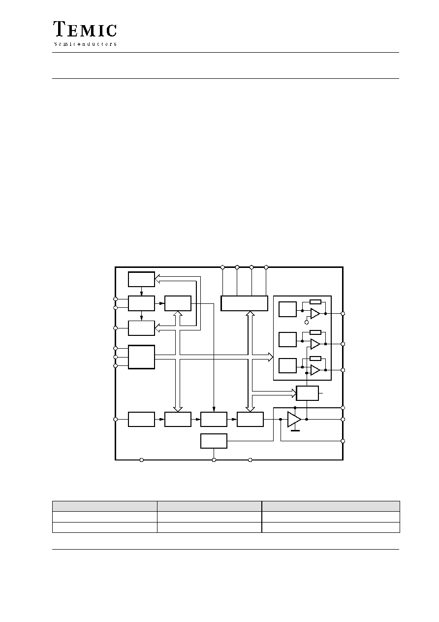
Block Diagram
FM≠
preamp
N≠
divider
Phase
detector
Current
sources
DAC1
AM/FM
DAC2
DAC3
3≠bit
VRef
SWO1 SWO2 SWO3 SWO4
Switching outputs
R≠
divider
Oscillator
OSC
buffer
3W≠
bus
interface
16
17
18
13
12
15
19
7
8
9
10
OSCIN
OSCOUT
MX2LO
CLK
DATA
EN
FMOSCIN
Band-gap
6
1
2
5
4
3
VRef
14
11
20
GNDan
V5
GND
96 11799
DAC3
DAC2
DAC1
VS
PDO
PD
Tuning
Figure 1. Block diagram
Ordering Information
Extended Type Number
Package
Remarks
U4256BM-AFS
SSO20
U4256BM-AFSG3
SSO20
Taped and reeled

U4256BM
Rev. A2, 03-Nov-98
Preliminary Information
2 (14)
Pin Description
1
2
3
4
5
6
7
8
13
14
15
16
17
18
19
20
U4256BM
EN
DATA
CLK
SWO1
SWO2
SWO3
SWO4
GNDan
OSCOUT
OSCIN
MX2LO
VS
PD
PDO
DAC2
V5
9
11
12
FMOSCIN
DAC1
GND
10
96 11944
DAC3
Figure 2. Pinning
Pin
Symbol
Function
¡¡¡
¡¡¡
1
¡¡¡¡¡
¡¡¡¡¡
PDO
¡¡¡¡¡¡¡¡¡¡
¡¡¡¡¡¡¡¡¡¡
Analog output
¡¡¡
¡¡¡
2
¡¡¡¡¡
¡¡¡¡¡
PD
¡¡¡¡¡¡¡¡¡¡
¡¡¡¡¡¡¡¡¡¡
Current output
¡¡¡
¡
¡
¡
¡¡¡
3
¡¡¡¡¡
¡
¡¡¡
¡
¡¡¡¡¡
DAC1
¡¡¡¡¡¡¡¡¡¡
¡
¡¡¡¡¡¡¡¡
¡
¡¡¡¡¡¡¡¡¡¡
Output 1,
digital to analog converter
¡¡¡
¡¡¡
4
¡¡¡¡¡
¡¡¡¡¡
DAC2
¡¡¡¡¡¡¡¡¡¡
¡¡¡¡¡¡¡¡¡¡
Output 2,
digital to analog converter
¡¡¡
¡
¡
¡
¡¡¡
5
¡¡¡¡¡
¡
¡¡¡
¡
¡¡¡¡¡
DAC3
¡¡¡¡¡¡¡¡¡¡
¡
¡¡¡¡¡¡¡¡
¡
¡¡¡¡¡¡¡¡¡¡
Output 3,
digital to analog converter
¡¡¡
¡¡¡
6
¡¡¡¡¡
¡¡¡¡¡
VS
¡¡¡¡¡¡¡¡¡¡
¡¡¡¡¡¡¡¡¡¡
Supply voltage analog part
¡¡¡
¡¡¡
7
¡¡¡¡¡
¡¡¡¡¡
SWO1
¡¡¡¡¡¡¡¡¡¡
¡¡¡¡¡¡¡¡¡¡
Switching output 1
¡¡¡
¡¡¡
8
¡¡¡¡¡
¡¡¡¡¡
SWO2
¡¡¡¡¡¡¡¡¡¡
¡¡¡¡¡¡¡¡¡¡
Switching output 2
¡¡¡
¡¡¡
9
¡¡¡¡¡
¡¡¡¡¡
SWO3
¡¡¡¡¡¡¡¡¡¡
¡¡¡¡¡¡¡¡¡¡
Switching output 3
¡¡¡
¡¡¡
10
¡¡¡¡¡
¡¡¡¡¡
SWO4
¡¡¡¡¡¡¡¡¡¡
¡¡¡¡¡¡¡¡¡¡
Switching output 4
¡¡¡
¡¡¡
11
¡¡¡¡¡
¡¡¡¡¡
GND
¡¡¡¡¡¡¡¡¡¡
¡¡¡¡¡¡¡¡¡¡
Ground, digital part
¡¡¡
12
¡¡¡¡¡
OSCOUT
¡¡¡¡¡¡¡¡¡¡
Oscillator output
¡¡¡
¡¡¡
13
¡¡¡¡¡
¡¡¡¡¡
OSCIN
¡¡¡¡¡¡¡¡¡¡
¡¡¡¡¡¡¡¡¡¡
Oscillator input
¡¡¡
¡¡¡
14
¡¡¡¡¡
¡¡¡¡¡
V5
¡¡¡¡¡¡¡¡¡¡
¡¡¡¡¡¡¡¡¡¡
Capacitor band gap
¡¡¡
¡¡¡
15
¡¡¡¡¡
¡¡¡¡¡
MX2LO
¡¡¡¡¡¡¡¡¡¡
¡¡¡¡¡¡¡¡¡¡
Oscillator buffer output
¡¡¡
¡¡¡
16
¡¡¡¡¡
¡¡¡¡¡
DATA
¡¡¡¡¡¡¡¡¡¡
¡¡¡¡¡¡¡¡¡¡
Data input
¡¡¡
¡¡¡
17
¡¡¡¡¡
¡¡¡¡¡
CLK
¡¡¡¡¡¡¡¡¡¡
¡¡¡¡¡¡¡¡¡¡
Clock
¡¡¡
¡¡¡
18
¡¡¡¡¡
¡¡¡¡¡
EN
¡¡¡¡¡¡¡¡¡¡
¡¡¡¡¡¡¡¡¡¡
Enable
¡¡¡
¡¡¡
19
¡¡¡¡¡
¡¡¡¡¡
FMOSCIN
¡¡¡¡¡¡¡¡¡¡
¡¡¡¡¡¡¡¡¡¡
FM-oscillator input
¡¡¡
¡¡¡
20
¡¡¡¡¡
¡¡¡¡¡
GNDan
¡¡¡¡¡¡¡¡¡¡
¡¡¡¡¡¡¡¡¡¡
Ground, analog part
Circuit Description
The U4256BM is a single chip PLL circuit, designed for
AM/FM RDS (Radio Data System) applications. The
special design allows to build automatic alignment tuner
systems. Two programmable DACs (Digital to Analog
Converter) support the computer controlled alignment.
The U4256BM has a very fast response time of maximum
800
ms (at 2 mA, fref = 100 kHz, measured on MPX
signal). It performs a high signal to noise ratio.
Only one supply voltage is necessary, due to a
integrated band gap.
The U4256BM is controlled via 3-wire bus.
Functional Description
The U4256BM is especially designed for AM up/down
converter systems, together with the tuner U4255BM.
Due to the integrated DACs, an automatic tuner
alignment is possible. All the functions of the U4256BM
can be software controlled via a serial 3-wire bus,
consisting of Enable, Clock and Data. The format and
procedure for the data transfer from the microcontroller
is shown in figures 3, 4 and table Data Transfer. All
requested data have to be transferred via 16-bit or 24-bit
commands. Due to the 8-bit structure, the serial output
interface of a microcontroller can be used for the data
transfer. The PLL functions can be controlled by 24-bit
commands, while the alignment functions are controlled
by 16-bit commands. The alignment function control
normally is set once by switching on the tuner. Then the
tuner automatically will be aligned. The data for
alignment are stored in a separate EPROM. Via integrated
capacitors it is possible to tune the reference oscillator
(this function is controlled via the 3-wire bus).

U4256BM
Preliminary Information
Rev. A2, 03-Nov-98
3 (14)
Absolute Maximum Ratings
All voltages are referred to GND (Pin 15)
Parameters
Symbol
Value
Unit
¡¡¡¡¡¡¡¡¡¡¡¡¡¡¡¡¡
¡¡¡¡¡¡¡¡¡¡¡¡¡¡¡¡¡
Analog supply voltage
Pin 6
¡¡¡¡¡
¡¡¡¡¡
V
S
¡¡¡¡¡¡¡¡
¡¡¡¡¡¡¡¡
8 to 15
¡¡¡¡¡
¡¡¡¡¡
V
¡¡¡¡¡¡¡¡¡¡¡¡¡¡¡¡¡
¡¡¡¡¡¡¡¡¡¡¡¡¡¡¡¡¡
Input voltage
Pins 16, 17 and 18
¡¡¡¡¡
¡¡¡¡¡
V
I
¡¡¡¡¡¡¡¡
¡¡¡¡¡¡¡¡
≠0.3 to +12
¡¡¡¡¡
¡¡¡¡¡
V
¡¡¡¡¡¡¡¡¡¡¡¡¡¡¡¡¡
¡¡¡¡¡¡¡¡¡¡¡¡¡¡¡¡¡
Output current
Pins 7, 8, 9 and 10
¡¡¡¡¡
¡¡¡¡¡
I
O
¡¡¡¡¡¡¡¡
¡¡¡¡¡¡¡¡
≠1 to +5
¡¡¡¡¡
¡¡¡¡¡
mA
¡¡¡¡¡¡¡¡¡¡¡¡¡¡¡¡¡
¡¡¡¡¡¡¡¡¡¡¡¡¡¡¡¡¡
Output drain voltage
Pins 7, 8, 9 and 10
¡¡¡¡¡
¡¡¡¡¡
V
OD
¡¡¡¡¡¡¡¡
¡¡¡¡¡¡¡¡
15
¡¡¡¡¡
¡¡¡¡¡
V
¡¡¡¡¡¡¡¡¡¡¡¡¡¡¡¡¡
¡¡¡¡¡¡¡¡¡¡¡¡¡¡¡¡¡
Ambient temperature range
¡¡¡¡¡
¡¡¡¡¡
T
amb
¡¡¡¡¡¡¡¡
¡¡¡¡¡¡¡¡
≠40 to +85
¡¡¡¡¡
¡¡¡¡¡
∞
C
¡¡¡¡¡¡¡¡¡¡¡¡¡¡¡¡¡
¡¡¡¡¡¡¡¡¡¡¡¡¡¡¡¡¡
Storage temperature range
¡¡¡¡¡
¡¡¡¡¡
T
stg
¡¡¡¡¡¡¡¡
¡¡¡¡¡¡¡¡
≠40 to +125
¡¡¡¡¡
¡¡¡¡¡
∞
C
¡¡¡¡¡¡¡¡¡¡¡¡¡¡¡¡¡
¡¡¡¡¡¡¡¡¡¡¡¡¡¡¡¡¡
Junction temperature
¡¡¡¡¡
¡¡¡¡¡
T
j
¡¡¡¡¡¡¡¡
¡¡¡¡¡¡¡¡
125
¡¡¡¡¡
¡¡¡¡¡
∞
C
¡¡¡¡¡¡¡¡¡¡¡¡¡¡¡¡¡
¡¡¡¡¡¡¡¡¡¡¡¡¡¡¡¡¡
Electrostatic handling
¡¡¡¡¡
¡¡¡¡¡
V
ESD
¡¡¡¡¡¡¡¡
¡¡¡¡¡¡¡¡
t.b.d.
¡¡¡¡¡
¡¡¡¡¡
V
Thermal Resistance
Parameters
Symbol
Value
Unit
Junction ambient
when soldered to PCB
R
thJA
140
K/W
Operating Range
All voltages are referred to GND (Pin 15)
Parameter
Symbol
Min.
Typ.
Max.
Unit
¡¡¡¡¡¡¡¡¡¡¡¡¡¡¡¡¡
¡¡¡¡¡¡¡¡¡¡¡¡¡¡¡¡¡
Supply voltage range
Pin 6
¡¡¡¡
¡¡¡¡
V
S
¡¡¡¡
¡¡¡¡
8
¡¡¡¡
¡¡¡¡
8.5
¡¡¡¡
¡¡¡¡
14
¡¡¡¡
¡¡¡¡
V
¡¡¡¡¡¡¡¡¡¡¡¡¡¡¡¡¡
¡¡¡¡¡¡¡¡¡¡¡¡¡¡¡¡¡
Ambient temperature
¡¡¡¡
¡¡¡¡
T
amb
¡¡¡¡
¡¡¡¡
≠40
¡¡¡¡
¡¡¡¡
¡¡¡¡
¡¡¡¡
+85
¡¡¡¡
¡¡¡¡
∞
C
¡¡¡¡¡¡¡¡¡¡¡¡¡¡¡¡¡
¡¡¡¡¡¡¡¡¡¡¡¡¡¡¡¡¡
Input frequency
Pin 19
¡¡¡¡
¡¡¡¡
RFi
¡¡¡¡
¡¡¡¡
70
¡¡¡¡
¡¡¡¡
¡¡¡¡
¡¡¡¡
160
¡¡¡¡
¡¡¡¡
MHz
¡¡¡¡¡¡¡¡¡¡¡¡¡¡¡¡¡
¡¡¡¡¡¡¡¡¡¡¡¡¡¡¡¡¡
Programmable divider
¡¡¡¡
¡¡¡¡
SF
¡¡¡¡
¡¡¡¡
2
¡¡¡¡
¡¡¡¡
¡¡¡¡
¡¡¡¡
65535
¡¡¡¡
¡¡¡¡
¡¡¡¡¡¡¡¡¡¡¡¡¡¡¡¡¡
¡¡¡¡¡¡¡¡¡¡¡¡¡¡¡¡¡
Crystal oscillator
Pins 12 and 13
¡¡¡¡
¡¡¡¡
fXTAL
¡¡¡¡
¡¡¡¡
0.1
¡¡¡¡
¡¡¡¡
¡¡¡¡
¡¡¡¡
15
¡¡¡¡
¡¡¡¡
MHz
Electrical Characteristics
Test conditions (unless otherwise specified): V
S
= +8.5 V, T
amb
= +25
∞
C
Parameters
Test Conditions / Pins
Symbol
Min.
Typ.
Max.
Unit
¡¡¡¡¡¡¡¡¡¡¡¡¡¡¡¡¡¡¡¡¡¡¡¡¡¡¡¡¡¡¡¡
¡¡¡¡¡¡¡¡¡¡¡¡¡¡¡¡¡¡¡¡¡¡¡¡¡¡¡¡¡¡¡¡
Supply voltage
Pin 6
¡¡¡¡¡¡¡¡¡¡¡
¡¡¡¡¡¡¡¡¡¡¡
Analog supply voltage
¡¡¡¡¡¡¡¡¡
¡¡¡¡¡¡¡¡¡
¡¡¡¡
¡¡¡¡
V
A
¡¡¡
¡¡¡
8
¡¡¡
¡¡¡
8.5
¡¡¡¡
¡¡¡¡
12
¡¡¡¡
¡¡¡¡
V
¡¡¡¡¡¡¡¡¡¡¡¡¡¡¡¡¡¡¡¡¡¡¡¡¡¡¡¡¡¡¡¡
¡¡¡¡¡¡¡¡¡¡¡¡¡¡¡¡¡¡¡¡¡¡¡¡¡¡¡¡¡¡¡¡
Supply current
Pin 20
¡¡¡¡¡¡¡¡¡¡¡
¡¡¡¡¡¡¡¡¡¡¡
Analog supply current
¡¡¡¡¡¡¡¡¡
¡¡¡¡¡¡¡¡¡
¡¡¡¡
¡¡¡¡
I
A
¡¡¡
¡¡¡
4.5
¡¡¡
¡¡¡
10
¡¡¡¡
¡¡¡¡
20
¡¡¡¡
¡¡¡¡
mA
¡¡¡¡¡¡¡¡¡¡¡¡¡¡¡¡¡¡¡¡¡¡¡¡¡¡¡¡¡¡¡¡
¡¡¡¡¡¡¡¡¡¡¡¡¡¡¡¡¡¡¡¡¡¡¡¡¡¡¡¡¡¡¡¡
OSCIN
Pin 13
¡¡¡¡¡¡¡¡¡¡¡
¡¡¡¡¡¡¡¡¡¡¡
Input voltage
¡¡¡¡¡¡¡¡¡
¡¡¡¡¡¡¡¡¡
f = 0.1 to 15 MHz
¡¡¡¡
¡¡¡¡
V
OSC
¡¡¡
¡¡¡
100
¡¡¡
¡¡¡
¡¡¡¡
¡¡¡¡
¡¡¡¡
¡¡¡¡
mV
rms
¡¡¡¡¡¡¡¡¡¡¡¡¡¡¡¡¡¡¡¡¡¡¡¡¡¡¡¡¡¡¡¡
¡¡¡¡¡¡¡¡¡¡¡¡¡¡¡¡¡¡¡¡¡¡¡¡¡¡¡¡¡¡¡¡
FMOSCIN
Pin 19
¡¡¡¡¡¡¡¡¡¡¡
¡¡¡¡¡¡¡¡¡¡¡
Input voltage
¡¡¡¡¡¡¡¡¡
¡¡¡¡¡¡¡¡¡
f = 70 to 120 MHz
f = 120 to 160 MHz
¡¡¡¡
¡¡¡¡
V
FMOSC
V
FMOSC
¡¡¡
¡¡¡
40
150
¡¡¡
¡¡¡
¡¡¡¡
¡¡¡¡
¡¡¡¡
¡¡¡¡
mV
rms
mV
rms
¡¡¡¡¡¡¡¡¡¡¡¡¡¡¡¡¡¡¡¡¡¡¡¡¡¡¡¡¡¡¡¡
¡¡¡¡¡¡¡¡¡¡¡¡¡¡¡¡¡¡¡¡¡¡¡¡¡¡¡¡¡¡¡¡
PD
Pin 2
¡¡¡¡¡¡¡¡¡¡¡
¡¡¡¡¡¡¡¡¡¡¡
Output current 1
¡¡¡¡¡¡¡¡¡
¡¡¡¡¡¡¡¡¡
PD = 2.5 V
¡¡¡¡
¡¡¡¡
¡¡¡
¡¡¡
20
¡¡¡
¡¡¡
25
¡¡¡¡
¡¡¡¡
30
¡¡¡¡
¡¡¡¡
µ
A
¡¡¡¡¡¡¡¡¡¡¡
¡¡¡¡¡¡¡¡¡¡¡
Output current 2
¡¡¡¡¡¡¡¡¡
¡¡¡¡¡¡¡¡¡
PD = 2.5 V
¡¡¡¡
¡¡¡¡
¡¡¡
¡¡¡
80
¡¡¡
¡¡¡
100
¡¡¡¡
¡¡¡¡
120
¡¡¡¡
¡¡¡¡
µ
A
¡¡¡¡¡¡¡¡¡¡¡
¡¡¡¡¡¡¡¡¡¡¡
Output current 3
¡¡¡¡¡¡¡¡¡
¡¡¡¡¡¡¡¡¡
PD = 2.5 V
¡¡¡¡
¡¡¡¡
±
IPD
¡¡¡
¡¡¡
400
¡¡¡
¡¡¡
500
¡¡¡¡
¡¡¡¡
600
¡¡¡¡
¡¡¡¡
µ
A
¡¡¡¡¡¡¡¡¡¡¡
¡¡¡¡¡¡¡¡¡¡¡
Output current 4
¡¡¡¡¡¡¡¡¡
¡¡¡¡¡¡¡¡¡
PD = 2.5 V
¡¡¡¡
¡¡¡¡
¡¡¡
¡¡¡
1600
¡¡¡
¡¡¡
2000
¡¡¡¡
¡¡¡¡
2400
¡¡¡¡
¡¡¡¡
µ
A
¡¡¡¡¡¡¡¡¡¡¡
¡¡¡¡¡¡¡¡¡¡¡
Leakage current
¡¡¡¡¡¡¡¡¡
¡¡¡¡¡¡¡¡¡
PD = 2.5 V
¡¡¡¡
¡¡¡¡
±
IPDL
¡¡¡
¡¡¡
¡¡¡
¡¡¡
¡¡¡¡
¡¡¡¡
20
¡¡¡¡
¡¡¡¡
nA

U4256BM
Rev. A2, 03-Nov-98
Preliminary Information
4 (14)
Electrical Characteristics (continued)
Test conditions (unless otherwise specified): V
S
= +8.5 V, T
amb
= +25
∞
C
Parameters
Test Conditions / Pins
Symbol
Min.
Typ.
Max.
Unit
¡¡¡¡¡¡¡¡¡¡¡¡¡¡¡¡¡¡¡¡¡¡¡¡¡¡¡¡¡¡¡¡
¡¡¡¡¡¡¡¡¡¡¡¡¡¡¡¡¡¡¡¡¡¡¡¡¡¡¡¡¡¡¡¡
PDO
Pin 1
¡¡¡¡¡¡¡¡¡¡¡
¡¡¡¡¡¡¡¡¡¡¡
Saturation voltage
HIGH
LOW
¡¡¡¡¡¡¡¡¡
¡¡¡¡¡¡¡¡¡
V
SATH
≠ (V
A
≠ V
PDOFM
),
I = 15 mA
¡¡¡¡
¡¡¡¡
V
SATH
V
SATL
¡¡¡
¡¡¡
100
¡¡¡
¡¡¡
200
¡¡¡¡
¡¡¡¡
500
400
¡¡¡¡
¡¡¡¡
mV
mV
¡¡¡¡¡¡¡¡¡¡¡¡¡¡¡¡¡¡¡¡¡¡¡¡¡¡¡¡¡¡¡¡
¡¡¡¡¡¡¡¡¡¡¡¡¡¡¡¡¡¡¡¡¡¡¡¡¡¡¡¡¡¡¡¡
SWO1, SWO2, SWO3, SWO4 (open drain)
Pins 7, 8, 9 and 10
¡¡¡¡¡¡¡¡¡¡¡
¡
¡¡¡¡¡¡¡¡¡
¡
¡¡¡¡¡¡¡¡¡¡¡
Output leakage current
HIGH
¡¡¡¡¡¡¡¡¡
¡
¡¡¡¡¡¡¡
¡
¡¡¡¡¡¡¡¡¡
I = 1 mA,
V7,8,9,10 = 8.5 V
¡¡¡¡
¡
¡¡
¡
¡¡¡¡
I
OHL
¡¡¡
¡¡
¡
¡¡¡
¡¡¡
¡
¡
¡
¡¡¡
¡¡¡¡
¡
¡¡
¡
¡¡¡¡
100
¡¡¡¡
¡
¡¡
¡
¡¡¡¡
nA
¡¡¡¡¡¡¡¡¡¡¡
¡¡¡¡¡¡¡¡¡¡¡
Output voltage
LOW
¡¡¡¡¡¡¡¡¡
¡¡¡¡¡¡¡¡¡
¡¡¡¡
¡¡¡¡
V
SWOL
¡¡¡
¡¡¡
¡¡¡
¡¡¡
100
¡¡¡¡
¡¡¡¡
400
¡¡¡¡
¡¡¡¡
mV
¡¡¡¡¡¡¡¡¡¡¡¡¡¡¡¡¡¡¡¡¡¡¡¡¡¡¡¡¡¡¡¡
DAC1, DAC2
Pins 3 and 4
¡¡¡¡¡¡¡¡¡¡¡
¡¡¡¡¡¡¡¡¡¡¡
Output current
¡¡¡¡¡¡¡¡¡
¡¡¡¡¡¡¡¡¡
¡¡¡¡
¡¡¡¡
I
DAC1, 2
¡¡¡
¡¡¡
¡¡¡
¡¡¡
¡¡¡¡
¡¡¡¡
1
¡¡¡¡
¡¡¡¡
mA
¡¡¡¡¡¡¡¡¡¡¡
¡¡¡¡¡¡¡¡¡¡¡
Output voltage
¡¡¡¡¡¡¡¡¡
¡¡¡¡¡¡¡¡¡
¡¡¡¡
¡¡¡¡
V
DAC1, 2
¡¡¡
¡¡¡
0.3
¡¡¡
¡¡¡
¡¡¡¡
¡¡¡¡
V
S
≠ 0.5
¡¡¡¡
¡¡¡¡
V
¡¡¡¡¡¡¡¡¡¡¡
¡¡¡¡¡¡¡¡¡¡¡
Gain range (resolution 256 steps)
¡¡¡¡¡¡¡¡¡
¡¡¡¡¡¡¡¡¡
¡¡¡¡
¡¡¡¡
¡¡¡
¡¡¡
0.6
¡¡¡
¡¡¡
¡¡¡¡
¡¡¡¡
2.3
¡¡¡¡
¡¡¡¡
¡¡¡¡¡¡¡¡¡¡¡
¡¡¡¡¡¡¡¡¡¡¡
Offset range (resolution 24 steps)
¡¡¡¡¡¡¡¡¡
¡¡¡¡¡¡¡¡¡
¡¡¡¡
¡¡¡¡
¡¡¡
¡¡¡
≠0.6
¡¡¡
¡¡¡
¡¡¡¡
¡¡¡¡
0.7
¡¡¡¡
¡¡¡¡
V
¡¡¡¡¡¡¡¡¡¡¡¡¡¡¡¡¡¡¡¡¡¡¡¡¡¡¡¡¡¡¡¡
¡¡¡¡¡¡¡¡¡¡¡¡¡¡¡¡¡¡¡¡¡¡¡¡¡¡¡¡¡¡¡¡
DAC 3
Pin 5
¡¡¡¡¡¡¡¡¡¡¡
¡¡¡¡¡¡¡¡¡¡¡
Output current
¡¡¡¡¡¡¡¡¡
¡¡¡¡¡¡¡¡¡
¡¡¡¡
¡¡¡¡
I
DAC3
¡¡¡
¡¡¡
¡¡¡
¡¡¡
¡¡¡¡
¡¡¡¡
1
¡¡¡¡
¡¡¡¡
mA
¡¡¡¡¡¡¡¡¡¡¡
¡¡¡¡¡¡¡¡¡¡¡
Output voltage (resolution 16 steps)
¡¡¡¡¡¡¡¡¡
¡¡¡¡¡¡¡¡¡
¡¡¡¡
¡¡¡¡
V
DAC3
¡¡¡
¡¡¡
0.25
¡¡¡
¡¡¡
¡¡¡¡
¡¡¡¡
6
¡¡¡¡
¡¡¡¡
V
¡¡¡¡¡¡¡¡¡¡¡¡¡¡¡¡¡¡¡¡¡¡¡¡¡¡¡¡¡¡¡¡
¡¡¡¡¡¡¡¡¡¡¡¡¡¡¡¡¡¡¡¡¡¡¡¡¡¡¡¡¡¡¡¡
MX2LO
¡¡¡¡¡¡¡¡¡¡¡
¡¡¡¡¡¡¡¡¡¡¡
Output AC voltage
¡¡¡¡¡¡¡¡¡
¡¡¡¡¡¡¡¡¡
At Pin15: 47 pF and 1 k
W
¡¡¡¡
¡¡¡¡
V
MX2LO
¡¡¡
¡¡¡
80
¡¡¡
¡¡¡
120
¡¡¡¡
¡¡¡¡
200
¡¡¡¡
¡¡¡¡
mV
pp
¡¡¡¡¡¡¡¡¡¡¡
¡¡¡¡¡¡¡¡¡¡¡
Output DC voltage
¡¡¡¡¡¡¡¡¡
¡¡¡¡¡¡¡¡¡
¡¡¡¡
¡¡¡¡
V
DC
¡¡¡
¡¡¡
1.6
¡¡¡
¡¡¡
1.9
¡¡¡¡
¡¡¡¡
2.1
¡¡¡¡
¡¡¡¡
V
3-Wire Bus Description
12
24-bit command
16-bit command
DATA
CLK
LSB
LSB
MSB
MSB
BYTE 1
BYTE 2
EN
EN
CLK
DATA
LSB
LSB
MSB
MSB
BYTE 3
BYTE 2
MSB
LSB
BYTE 1
EN
e.g., Divider
0
0
2
0
2
1
2
2
2
3
2
4
2
5
2
6
2
7
2
8
2
9
2
10
2
11
2
2
13
IPD3
P≠2
1
R≠Divider
Addr.
P≠2
0
P≠2
2
14858
Status 0
OSCB
IPD1
2
14
2
15
IPD4 IPD2
Figure 3. Pulse diagram

U4256BM
Preliminary Information
Rev. A2, 03-Nov-98
5 (14)
Data Transfer
A
¡¡¡¡¡¡¡¡¡¡¡
¡¡¡¡¡¡¡¡¡¡¡
MSB BYTE 2 LSB
¡¡¡¡¡¡¡¡¡¡¡¡¡
¡¡¡¡¡¡¡¡¡¡¡¡¡
MSB BYTE 1 LSB
¡¡¡¡¡¡¡¡¡¡¡¡¡¡¡¡¡¡¡¡¡¡¡
¡¡¡¡¡¡¡¡¡¡¡¡¡¡¡¡¡¡¡¡¡¡¡
ADDR. Oscillator tuning function
¡¡
1
¡
0
¡¡¡
8pF
¡¡
32pF
¡¡¡
16pF
¡¡
8pF
¡¡¡
4pF
¡¡
2pF
¡¡¡
1pF
¡¡
0.5pF
¡¡¡
¡¡
¡¡¡
¡¡
¡¡¡
¡¡
¡¡
¡¡
¡
¡
¡¡¡
¡¡¡
B85
¡¡
¡¡
B84
¡¡¡
¡¡¡
B83
¡¡
¡¡
B82
¡¡¡
¡¡¡
B81
¡¡
¡¡
B80
¡¡¡
¡¡¡
B79
¡¡
¡¡
B78
¡¡¡
¡¡¡
B77
¡¡
¡¡
B76
¡¡¡
¡¡¡
B75
¡¡
¡¡
B74
¡¡¡
¡¡¡
B73
¡¡
¡¡
B72
B
¡¡¡¡¡¡¡¡¡¡¡
¡¡¡¡¡¡¡¡¡¡¡
MSB Byte 3 LSB
¡¡¡¡¡¡¡¡¡¡¡¡
¡¡¡¡¡¡¡¡¡¡¡¡
MSB BYTE 2 LSB
¡¡¡¡¡¡¡¡¡¡¡
¡¡¡¡¡¡¡¡¡¡¡
MSB BYTE 1 LSB
¡¡¡¡¡¡¡¡¡¡¡¡¡¡¡¡¡¡¡¡¡¡¡¡¡¡¡¡¡¡¡¡
¡¡¡¡¡¡¡¡¡¡¡¡¡¡¡¡¡¡¡¡¡¡¡¡¡¡¡¡¡¡¡¡
ADDR. STATUS 0 R ≠ DIVIDER
¡¡
¡¡
0
¡
¡
0
¡¡¡
¡¡¡
IPD
1,2
¡¡
¡¡
IPD
3,4
¡¡¡
¡¡¡
OSCB
0 = on,
1 = off
¡¡¡
¡¡¡
P≠2
2
¡¡
¡¡
P≠2
1
¡¡
¡¡
P≠2
0
¡¡¡
¡¡¡
2
15
¡¡
¡¡
2
14
¡¡
¡¡
2
13
¡¡¡
¡¡¡
2
12
¡¡
¡¡
2
11
¡¡
¡¡
2
10
¡¡
¡¡
2
9
¡¡¡
¡¡¡
2
8
¡¡
¡¡
2
7
¡¡
¡¡
2
6
¡¡
¡¡
2
5
¡¡¡
¡¡¡
2
4
¡¡
¡¡
2
3
¡¡
¡¡
2
2
¡¡¡
¡¡¡
2
1
¡¡
¡¡
2
0
¡¡
¡¡
¡
¡
¡¡¡
¡¡¡
B71
¡¡
¡¡
B70
¡¡¡
¡¡¡
B69
¡¡¡
¡¡¡
B68
¡¡
¡¡
B67
¡¡
¡¡
B66
¡¡¡
¡¡¡
B65
¡¡
¡¡
B64
¡¡
¡¡
B63
¡¡¡
¡¡¡
B62
¡¡
¡¡
B61
¡¡
¡¡
B60
¡¡
¡¡
B59
¡¡¡
¡¡¡
B58
¡¡
¡¡
B57
¡¡
¡¡
B56
¡¡
¡¡
B55
¡¡¡
¡¡¡
B54
¡¡
¡¡
B53
¡¡
¡¡
B52
¡¡¡
¡¡¡
B51
¡¡
¡¡
B50
C
¡¡¡¡¡¡¡¡¡¡¡
¡¡¡¡¡¡¡¡¡¡¡
MSB BYTE 2 LSB
¡¡¡¡¡¡¡¡¡¡¡¡
¡¡¡¡¡¡¡¡¡¡¡¡
MSB BYTE 1 LSB
¡¡¡¡¡¡¡¡¡¡¡¡¡¡¡¡¡¡¡¡¡¡
¡¡¡¡¡¡¡¡¡¡¡¡¡¡¡¡¡¡¡¡¡¡
ADDR. DAC1 ≠ GAIN & OFFSET
¡¡
0
¡
0
¡¡¡
O≠2
5
¡¡
O≠2
4
¡¡¡
O≠2
3
¡¡
O≠2
2
¡¡
O≠2
1
¡¡¡
O≠2
0
¡¡
G≠2
7
¡¡¡
G≠2
6
¡¡
G≠2
5
¡¡¡
G≠2
4
¡¡
G≠2
3
¡¡¡
G≠2
2
¡¡
G≠2
1
¡¡
G≠2
0
¡¡
¡¡
¡
¡
¡¡¡
¡¡¡
B49
¡¡
¡¡
B48
¡¡¡
¡¡¡
B47
¡¡
¡¡
B46
¡¡
¡¡
B45
¡¡¡
¡¡¡
B44
¡¡
¡¡
B43
¡¡¡
¡¡¡
B42
¡¡
¡¡
B41
¡¡¡
¡¡¡
B40
¡¡
¡¡
B39
¡¡¡
¡¡¡
B38
¡¡
¡¡
B37
¡¡
¡¡
B36
D
¡¡¡¡¡¡¡¡¡¡¡¡¡
¡¡¡¡¡¡¡¡¡¡¡¡¡
MSB Byte 3 LSB
¡¡¡¡¡¡¡¡¡¡¡
¡¡¡¡¡¡¡¡¡¡¡
MSB BYTE 2 LSB
¡¡¡¡¡¡¡¡¡¡¡
¡¡¡¡¡¡¡¡¡¡¡
MSB BYTE 1 LSB
¡¡¡¡¡¡¡¡¡¡¡¡¡¡¡¡¡¡¡¡¡¡¡¡¡¡¡¡¡¡¡¡¡
¡¡¡¡¡¡¡¡¡¡¡¡¡¡¡¡¡¡¡¡¡¡¡¡¡¡¡¡¡¡¡¡¡
ADDR. STATUS 1 N ≠ DIVIDER
¡¡
¡¡
0
¡
¡
1
¡¡¡
¡¡¡
0
¡¡¡
¡¡¡
AM = 1
FM = 0
¡¡
¡¡
SWO4
1=off,
0=on
¡¡¡
¡¡¡
SWO3
1=off,
0=on
¡¡¡
¡¡¡
SWO2
1=off,
0=on
¡¡¡
¡¡¡
SWO1
1=off,
0=on
¡¡¡
¡¡¡
2
15
¡¡
¡¡
2
14
¡¡
¡¡
2
13
¡¡
¡¡
2
12
¡¡¡
¡¡¡
2
11
¡¡
¡¡
2
10
¡¡
¡¡
2
9
¡¡
¡¡
2
8
¡¡¡
¡¡¡
2
7
¡¡
¡¡
2
6
¡¡
¡¡
2
5
¡¡
¡¡
2
4
¡¡¡
¡¡¡
2
3
¡¡
¡¡
2
2
¡¡
¡¡
2
1
¡¡
¡¡
2
0
¡¡
¡¡
¡
¡
¡¡¡
¡¡¡
B35
¡¡¡
¡¡¡
B34
¡¡
¡¡
B33
¡¡¡
¡¡¡
B32
¡¡¡
¡¡¡
B31
¡¡¡
¡¡¡
B30
¡¡¡
¡¡¡
B29
¡¡
¡¡
B28
¡¡
¡¡
B27
¡¡
¡¡
B25
¡¡¡
¡¡¡
B24
¡¡
¡¡
B23
¡¡
¡¡
B22
¡¡
¡¡
B22
¡¡¡
¡¡¡
B21
¡¡
¡¡
B20
¡¡
¡¡
B19
¡¡
¡¡
B18
¡¡¡
¡¡¡
B17
¡¡
¡¡
B16
¡¡
¡¡
B15
¡¡
¡¡
B14
E
¡¡¡¡¡¡¡¡¡¡¡
¡¡¡¡¡¡¡¡¡¡¡
MSB BYTE 2 LSB
¡¡¡¡¡¡¡¡¡¡¡¡
¡¡¡¡¡¡¡¡¡¡¡¡
MSB BYTE 1 LSB
¡¡¡¡¡¡¡¡¡¡¡¡¡¡¡¡¡¡¡¡¡¡
¡¡¡¡¡¡¡¡¡¡¡¡¡¡¡¡¡¡¡¡¡¡
ADDR. DAC2 ≠ GAIN & OFFSET
¡¡
0
¡
1
¡¡¡
O≠2
5
¡¡
O≠2
4
¡¡¡
O≠2
3
¡¡
O≠2
2
¡¡
O≠2
1
¡¡¡
O≠2
0
¡¡
G≠2
7
¡¡¡
G≠2
6
¡¡
G≠2
5
¡¡¡
G≠2
4
¡¡
G≠2
3
¡¡¡
G≠2
2
¡¡
G≠2
1
¡¡
G≠2
0
¡¡
¡¡
¡
¡
¡¡¡
¡¡¡
B13
¡¡
¡¡
B12
¡¡¡
¡¡¡
B11
¡¡
¡¡
B10
¡¡
¡¡
B9
¡¡¡
¡¡¡
B8
¡¡
¡¡
B7
¡¡¡
¡¡¡
B6
¡¡
¡¡
B5
¡¡¡
¡¡¡
B4
¡¡
¡¡
B3
¡¡¡
¡¡¡
B2
¡¡
¡¡
B1
¡¡
¡¡
B0