U4283BM
Preliminary Information
TELEFUNKEN Semiconductors
Rev. A1, 15-May-96
1 (9)
AM / FM - PLL
Description
The U4283BM is an integrated circuit in BICMOS
technology for frequency synthesizer. It performs all the
functions of a PLL radio tuning system and is controlled
by I
2
C bus. The device is designed for all frequency
synthesizer applications of radio receivers, as well as
RDS (Radio Data System) applications.
Features
D Reference oscillator up to 15 MHz
D Two programmable 16 bit dividers
adjustable from 2 to 65535
D Fine tuning steps:
AM
y 1 kHz
FM
y 2 kHz
D Three programmable switching outputs
(open drain up to 20 V)
D Few external component requirements due
to integrated loop-transistor for AM/FM
D High signal/ noise ratio
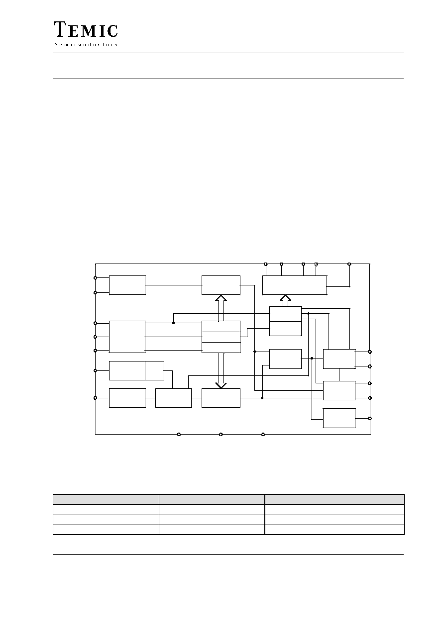
Block Diagram
16
Shift register
Latch
Latch
Preamplifier
R-Divider
N�Divider
Preamplifier
: 2
Oscillator
Status
Latch
detector
Phase
Current
sources
Analogue
outputs
Switching outputs
14
PDFM
15
PDAM
13
PDFMO
PDAMO
11
1
DD
V
20
GND 2
GND 1
10
FMOSC
12
AMOSC
2
3
SDA
SCL
4
AS
18
19
OSCIN
OSCOUT
5
SWO1
8
SWO3
94 8054 e
AM/FM
switch
I
2
C�BUS
Interface
6
7
9
AM/FM
SWO2
PRT
17
LD
Lock
detector
Figure 1.
Ordering and Package Information
Extended Type Number
Package
Remarks
U4283BM-BFL
SO20 plastic
U4283BM-BFLG3
SO20 plastic
Taping according to IEC-286-3
U4283BM-BFS
SSO20 plastic
U4283BM
TELEFUNKEN Semiconductors
Rev. A1, 15-May-96
Preliminary Information
2 (9)
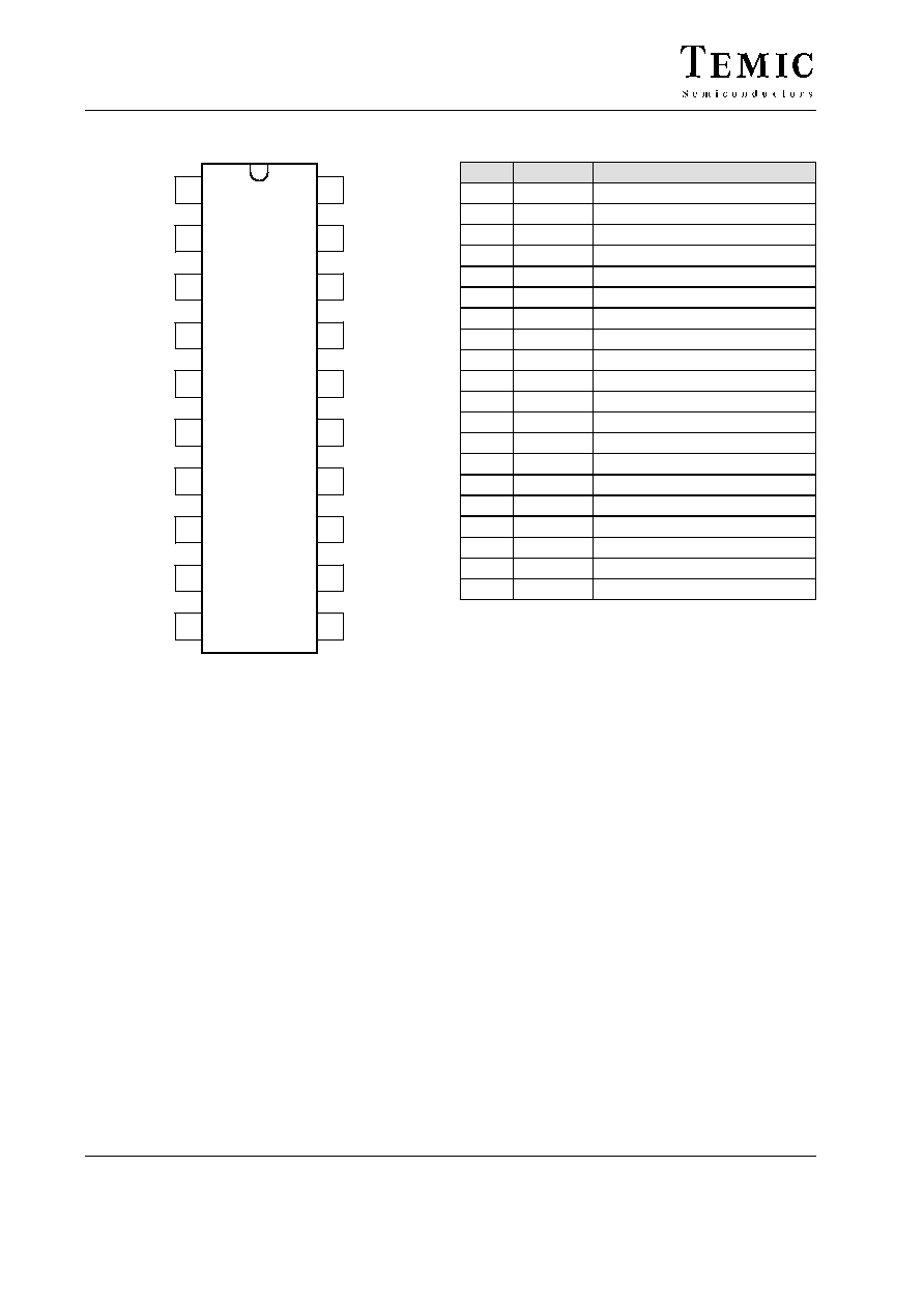
Pin Description
1
2
3
4
5
6
7
8
9
10
11
12
13
14
15
16
U4283BM
SCL
SDA
AS
SWO 1
SWO 2
FMOSC
GND1
OSCOUT
OSCIN
LD
PDAM
PDFM
PDFMO
AMOSC
V
DD
94 8055 e
17
18
19
20
GND2
PDAMO
SWO 3
AM/FM
PRT
Pin
Symbol
Function
1
V
DD
Supply voltage
2
SCL
I
2
C bus clock
3
SDA
I
2
C bus data
4
AS
Address selection
5
PRT
Switching port
6
SWO 1
Switching output 1
7
SWO 2
Switching output 2
8
SWO3
Switching output 3
9
AM/FM
Switching output AM/FM
10
FMOSC
FM oscillator input
11
GND 2
Ground 2 (analogue)
12
AMOSC
AM oscillator input
13
PDFMO
FM analogue output
14
PDFM
FM current output
15
PDAM
AM current output
16
PDAMO
AM analogue output
17
LD
Lock detector
18
OSCIN
Oscillator input
19
OSCOUT Oscillator output
20
GND 1
Ground 1 (digital)
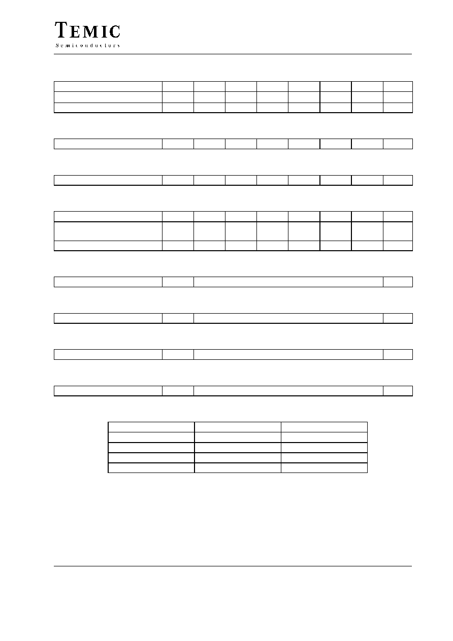
Functional Description
The U4283BM is controlled via the 2-wire I
2
C bus. For
programming there are one module address byte, two
subaddress bytes and five data bytes.
The module address contains a programmable address bit
A 1 which with address select input AS (Pin 4) makes it
possible to operate two U4283BM-B in one system. If bit
A 1 is identical with the status of the address select input
AS, the chip is selected.
The subaddress determines which one of the data bytes is
transmitted first. If subaddress of R-divider is
transmitted, the sequence of the next data bytes is DB 0
(Status), DB 1 and DB 2.
If subaddress of N-divider is transmitted, the sequence of
the next data bytes is DB 3 and DB 4. The bit organisation
of the module address, subaddress and 5 data bytes are
shown in figure 2
Each transmission on the I
2
C bus begins with the
"START "-condition and has to be ended by the "STOP"-
condition (see figure 3).
The integrated circuit U 4283 BM has two separate inputs
for AM and FM oscillator. Pre-amplified AM signal is
directed to the 16 bit N-divider via AM/FM switch,
whereas (pre-amplified) FM signal is first divided by a
fixed prescaler ( :2 ). AM/FM switch is controlled by
software. Tuning steps can be selected by 16 bit
R-divider. Further there is a digital memory phase
detector. There are two separate current sources for AM
and FM amplifier (charge pump) as given in electrical
characteristics. It allows independent adjustment of gain,
whereby providing high current for high speed tuning and
low current for stable tuning.
U4283BM
Preliminary Information
TELEFUNKEN Semiconductors
Rev. A1, 15-May-96
3 (9)
Bit Organization
MSB
LSB
Module address
1
1
0
0
1
0
0/1
0
A7
A6
A5
A4
A3
A2
A1
A0
Subaddress (R-divider)
X
X
X
X
0
1
X
X
Subaddress (N-divider)
X
X
X
X
1
1
X
X
MSB
LSB
Data byte 0 (Status)
PRT
SWO1
SWO2
SWO3
AM/
FM
PD
ANA
PD
POL
PD
CUR
D7
D6
D5
D4
D3
D2
D1
D0
Data byte 1
2
15
R-divider
2
8
Data byte 2
2
7
R-divider
2
0
Data byte 3
2
15
N-divider
2
8
Data byte 4
2
7
N-divider
2
0
LOW
HIGH
AM/FM
FM-operation
AM-operation
PD - ANA
PD analog
TEST
PD - POL
Negative polarity
Positive polarity
PD - CUR
Output current 2
Output current 1
Figure 2.
U4283BM
TELEFUNKEN Semiconductors
Rev. A1, 15-May-96
Preliminary Information
4 (9)
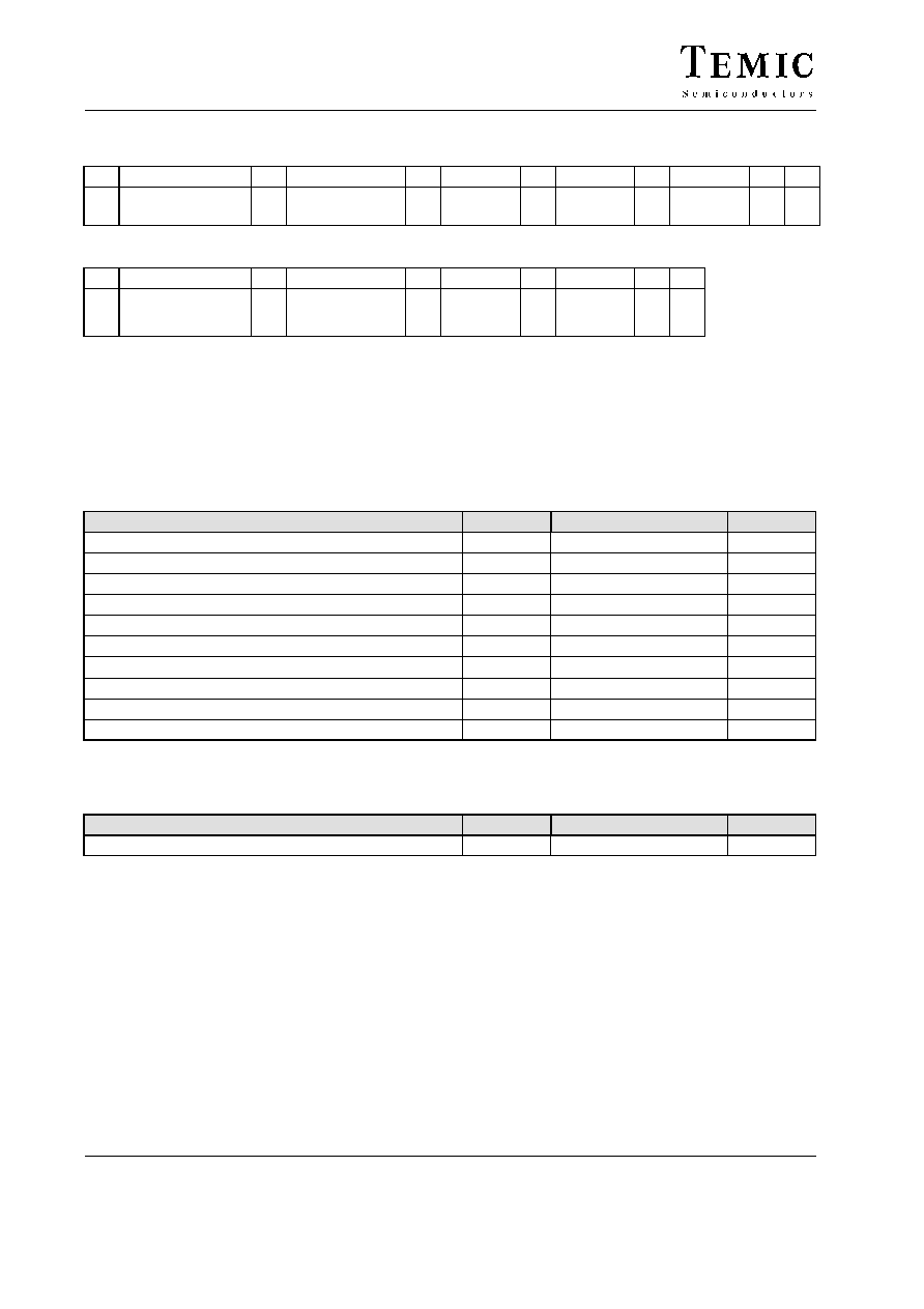
Transmission Protocol
MSB LSB
S
Address
A7 A0
A
Subaddress
R-divider
A
Data 0
A
Data 1
A
Data 2
A
P
MSB LSB
S
Address
A7 A0
A
Subaddress
N-divider
A
Data 3
A
Data 4
A
A
P
S = Start
P = Stop
A = Acknowledge
Figure 3.
Absolute Maximum Ratings
Parameters
Symbol
Value
Unit
Supply voltage
Pin 1
V
DD
�0.3 to +6
V
Input voltage
Pins 2, 3, 4, 10, 12, 18 and 19
V
I
�0.3 to V
DD
+0.3
V
Output current
Pins 3, 5, 6, 7, 8 and 9
I
O
�1 to +5
mA
Output drain voltage
Pins 6, 7, 8 and 9
V
OD
20
V
Output voltage
Pins 13 and 16
V
AO
15
V
Output current
Pins 13 and 16
I
AO
�1 to +20
mA
Ambient temperature range
T
amb
�25 to
+85
_C
Storage temperature range
T
stg
�40 to
+125
_C
Junction temperature
T
j
125
_C
Electrostatic handling (MIL Standard 883C)
"V
ESD
2000
V
Thermal Resistance
Parameters
Symbol
Value
Unit
Junction ambient
R
thJA
160
K/W
U4283BM
Preliminary Information
TELEFUNKEN Semiconductors
Rev. A1, 15-May-96
5 (9)
Electrical Characteristics
V
DD
= 5 V, T
amb
= 25
�
C, unless otherwise specified.
Parameters
Test Conditions / Pins
Symbol
Min.
Typ.
Max.
Unit
Supply voltage
Pin 1
V
DD
4.5
5.0
5.5
V
Quiescent supply current
Pin 1
I
DD
6.0
11.6
mA
FM input sensitivity, R
G
= 50
W FMOSC
f
i
= 70 to 120 MHz
Pin 10
V
SFM
25
mV
f
i
= 120 to 130 MHz
Pin 10
V
SFM
50
mV
AM input sensitivity, R
G
= 50
W AMOSC
f
i
= 0.5 to 35 MHz
Pin 12
V
SAM
25
mV
Oscillator input sensitivity, R
G
= 50
W OSCIN
f
i
= 0.1 to 15 MHz
Pin 14
V
SOSC
100
mV
Switching output SWO 1, SWO 2, SWO3, AM/FM (open drain)
Output voltage
LOW
LOW
Output leakage current
HIGH
Pins 6, 7, 8 and 9
I
L
= 1 mA
I
L
= 0.1 mA
Pins 6, 7, 8 and 9
V5, V6 = 20 V
V
SWOL
V
SWOL
I
OHL
200
20
400
100
100
mV
mV
nA
Lock detector output (open drain)
Output voltage
LOW
I = 3 mA
0.4
V
Switching output PRT
Pin 5
Output voltage
HIGH
LOW
LOW
I
L
= 1 mA
I
L
= 1 mA
I
L
= 0.1 mA
V
OH
V
OL
V
OL
V
DD
�0.4
0.4
0.1
V
V
V
Phase detector PDFM
Output current 1
Output current 2
Pin 14
Pin 14
"I
PDFM
"I
PDFM
400
100
500
125
600
150
mA
mA
Phase detector PDAM
Output current 1
Output current 2
Pin 15
Pin 15
"I
PDAM
"I
PDAM
75
20
100
25
125
30
mA
mA
Analogue output PDFMO, PDAMO
Saturation voltage
I = 15 mA
Pins 13 and 16
V
sat
270
400
mV
Leakage current
Pins 13 and 16
I
LEAK
1
mA
I
2
C bus SCL, SDA, AS
Input voltage
HIGH
LOW
Pins 2, 3 and 4
V
iBUS
3.0
0
V
DD
1.5
V
V
Output voltage
Acknowledge LOW
I
SDA
= 3 mA
Pin 3
V
O
0.4
V
Clock frequency
Pin 2
f
SCL
100
kHz
Rise time SDA, SCL
Pins 2 and 3
t
r
1
ms