
U4285BM
TELEFUNKEN Semiconductors
Rev. A3, 14-May-97
1 (10)
AM / FM - PLL
Description
The U4285BM is an integrated circuit in BICMOS
technology for frequency synthesizers. It performs all the
functions of a PLL radio tuning system and is controlled
by an I
2
C bus. The device is designed for all frequency
synthesizer applications in radio receivers, as well as
RDS ( Radio Data System ) applications.
Features
D Reference oscillator up to 15 MHz
D Two programmable 16 bit dividers
adjustable from 2 to 65535
D Fine tuning steps:
AM
y 1 kHz
FM
y 2 kHz
D 4 programmable switching outputs
(open drain up to 15 V)
D Few external component required due to
integrated loop-push-pull stage for AM/FM
D High signal/ noise ratio
Ordering Information
Extended Type Number
Package
Remarks
U4285BM-AFS
SSO20 plastic
U4285BM-AFSG3
SSO20 plastic
Taping according to IEC-286-3
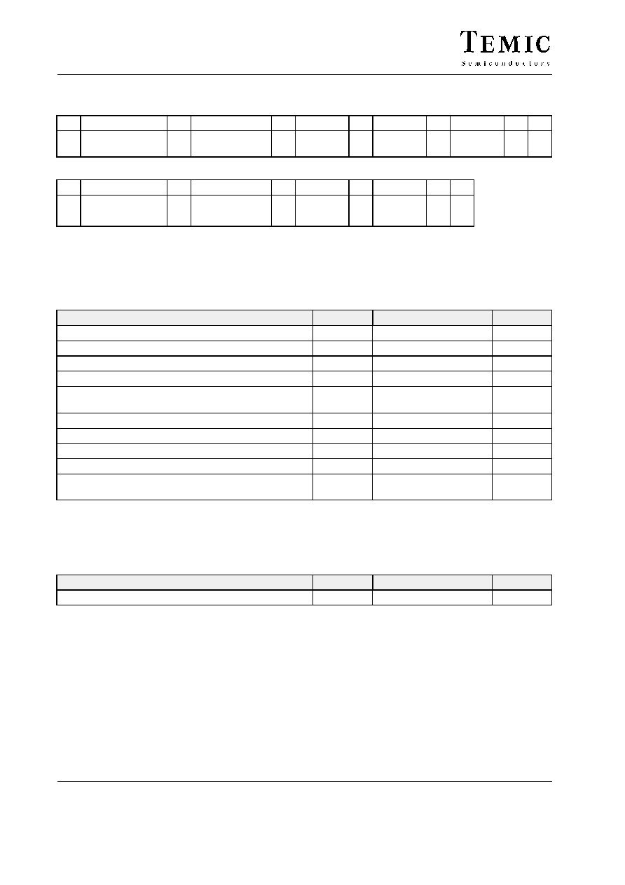
Block Diagram
R-divider
N-divider
I
2
C bus
interface
Oscillator
Phase
Current
sources
Switching outputs
AM/FM
18
19
2
3
4
9
11
OSCOUT
OSCIN
SCL
AS
FMOSC
AMOSC
SDA
5
6
7
8
10
1
20
SWO1
SWO4
SWO2 SWO3
14
15
16
17
12
13
PDAM
PDAMO
VA
C
PDFMO
PDFM
GND2
GND1
DD
V
95 10120
switch
detector
Figure 1.

U4285BM
TELEFUNKEN Semiconductors
Rev. A3, 14-May-97
2 (10)
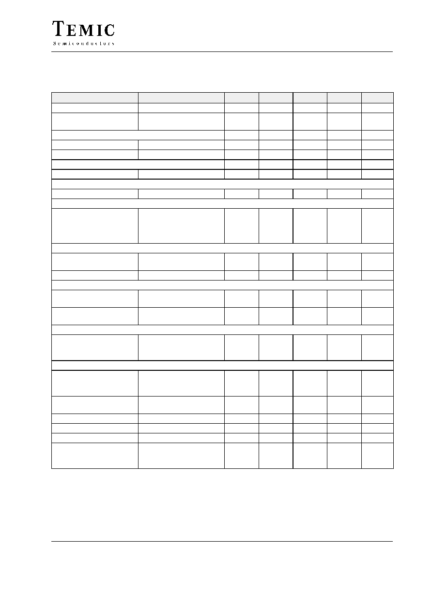
Pin Description
1
2
3
4
5
6
7
8
13
14
15
16
17
18
19
20
U4285BM
SCL
SDA
AS
SWO 1
SWO 2
SWO3
SWO4
GND1
OSCOUT
OSCIN
C
VA
PDAMO
PDAM
PDFM
V
DD
9
11
12
FMOSC
GND 2
PDFMO
AMOSC
10
95 10121
Pin
Symbol
Function
1
V
DD
Supply voltage
2
SCL
I
2
C bus clock
3
SDA
I
2
C bus data
4
AS
Address selection
5
SWO 1
Switching output 1
6
SWO 2
Switching output 2
7
SWO3
Switching output 3
8
SWO4
Switching output 4
9
FMOSC
FM oscillator input
10
GND 2
Ground 2 (analog)
11
AMOSC
AM oscillator input
12
PDFMO
FM analogue output
13
PDFM
FM current output
14
PDAM
AM current output
15
PDAMO
AM analogue output
16
VA
Analogue supply voltage
17
C
Capacitor
18
OSCIN
Oscillator input
19
OSCOUT Oscillator output
20
GND1
Ground 1 (digital)
Functional Description
The U4285BM is controlled via the 2-wire I
2
C bus. For
programming there are one module address byte, two sub-
address bytes and five data bytes.
The module address contains a programmable address bit
A 1 which with address select input AS (Pin 4) makes it
possible to operate two U4285BM in one system. If bit
A 1 is identical with the status of the address select input
AS, the chip is selected .
The subaddress determines which one of the data bytes is
transmitted first. If subaddress of R-divider is trans-
mitted, the sequence of the next data bytes is DB 0
(Status), DB 1 and DB 2.
If subaddress of N-divider is transmitted, the sequence of
the next data bytes is DB 3 and DB 4. The bit organisation
of the module address, subaddress and 5 data bytes are
shown in figure 2.
Each transmission on the I
2
C bus begins with the
"START"- condition and has to be ended by the "STOP"-
condition (see figure 3).
The integrated circuit U4285BM has two separate inputs
for AM and FM oscillator. Pre-amplified AM and FM
signals are fed to the 16 bit N-divider via AM/FM switch.
AM/FM switch is controlled by software. Tuning steps
can be selected by 16 bit R-divider. Further there is a
digital memory phase detector. There are two separate
current sources for AM and FM amplifier (charge pump)
as given in electrical characterisitics. It allows indepen-
dent adjustment of gain, whereby providing high current
for high speed tuning and low current for stable tuning.

U4285BM
TELEFUNKEN Semiconductors
Rev. A3, 14-May-97
3 (10)
Bit Organization
MSB
LSB
Module address
1
1
0
0
1
0
0/1
0
A7
A6
A5
A4
A3
A2
A1
A0
Subaddress (R-divider)
X
X
X
0
0
1
X
X
Subaddress (N-divider)
X
X
X
X
1
1
X
X
MSB
LSB
Data byte 0 (Status)
SWO1
SWO2
SWO3
SWO4
AM/
FM
PD
ANA
PD
POL
PD
CUR
D7
D6
D5
D4
D3
D2
D1
D0
Data byte 1
2
15
R-divider
2
8
Data byte 2
2
7
R-divider
2
0
Data byte 3
2
15
N-divider
2
8
Data byte 4
2
7
N-divider
2
0
LOW
HIGH
AM/FM
FM-operation
AM-operation
PD � ANA
PD analog
TEST
PD � POL
Negative polarity
Positive polarity
PD � CUR
Output current 2
Output current 1
Figure 2.
U4285BM
TELEFUNKEN Semiconductors
Rev. A3, 14-May-97
4 (10)
Transmission Protocol
MSB
LSB
S
Address
A7 A0
A
Subaddress
R-divider
A
Data 0
A
Data 1
A
Data 2
A
P
MSB
LSB
S
Address
A7 A0
A
Subaddress
N�divider
A
Data 3
A
Data 4
A
A
P
S = Start
P = Stop
A = Acknowledge
Figure 3.
Absolute Maximum Ratings
Parameters
Symbol
Value
Unit
Supply voltage
Pin 1
V
DD
�0.3 to +6
V
Input voltage
Pins 2, 3, 4, 9, 11, 18 and 19
V
I
�0.3 to V
DD
+ 0.3
V
Output current
Pins 3, 5, 6, 7 and 8
I
O
�1 to
+5
mA
Output drain voltage
Pins 5, 6, 7 and 8
V
OD
15
V
Analogue supply voltage
Pin 16
with 220
W seriell resistance 2 minutes
1
V
A
V
A
6 to 15
24
V
V
Output current
Pins 12 and 15
I
AO
�1 to
+20
mA
Ambient temperature range
T
amb
�30 to
+85
_C
Storage temperature range
T
stg
�40 to
+125
_C
Junction temperature
T
j
125
_C
Electrostatic handling (modified MIL STD 883 D
method 3015.7: all supply pins connected together)
"V
ESD
1000
V
1
corresponding our application circuit (page 8)
Thermal Resistance
Parameters
Symbol
Value
Unit
Junction ambient
R
thJA
160
K/W
U4285BM
TELEFUNKEN Semiconductors
Rev. A3, 14-May-97
5 (10)
Electrical Characteristics
V
DD
= 5 V, V
A
= 10 V, T
amb
= 25
�
C, unless otherwise specified
Parameters
Test conditions / Pin
Symbol
Min.
Typ.
Max.
Unit
Supply voltage
Pin 1
V
DD
4.5
5.0
5.5
V
Quiescent supply current
AM-mode
Pin 1
FM-mode
I
DD
4.0
4.0
7.0
7.0
mA
FM input sensitivity, R
G
= 50
W FMOSC
f
i
= 70 to 120 MHz
Pin 9
V
SFM
40
mV
rms
f
i
= 160 MHz
Pin 9
V
SFM
150
mV
rms
AM input sensitivity, R
G
= 50
W AMOSC
f
i
= 0.6 to 35 MHz
Pin 11
V
SAM
40
mV
rms
Oscillator input sensitivity, R
G
= 50
W OSCIN
f
i
= 0.1 to 15 MHz
Pin 18
V
SOSC
100
mV
rms
Switching output SWO 1, SWO 2, SWO 3, SWO 4 (open drain)
Output voltage
LOW
Output leakage current
HIGH
Pins 5, 6, 7 and 8
I
L
= 1 mA
Pins 5, 6, 7 and 8
V5, V6, V7, V8 = 10 V
V
SWOL
I
OHL
100
400
100
mV
nA
Phase detector PDFM
Output current 1
Output current 2
Pin 13
Pin 13
"I
PDFM
"I
PDFM
1600
400
2000
500
2400
600
mA
mA
Leakage current
Pin 13
"I
PDFML
20
nA
Phase detector PDAM
Output current 1
Output current 2
Pin 14
Pin 14
"I
PDAM
"I
PDAM
160
40
200
50
240
60
mA
mA
Leakage current
Pin 14
"I
PDAM-
L
20
nA
Analogue output PDFMO, PDAMO
Saturation voltage
LOW
HIGH
Pins 12 and 15
I = 15 mA
V
satL
V
satH
9.5
200
9.95
400
mV
V
I
2
C bus SCL, SDA, AS
Input voltage
HIGH
LOW
Pins 2, 3 and 4
V
iBUS
3.0
0
V
DD
1.5
V
V
Output voltage
Acknowledge LOW
Pin 3
I
SDA
= 3 mA
V
O
0.4
V
Clock frequency
Pin 2
f
SCL
100
kHz
Rise time SDA, SCL
Pins 2 and 3
t
r
1
ms
Fall time SDA, SCL
Pins 2 and 3
t
f
300
ns
Period of SCL
HIGH
LOW
Pin 2
HIGH
LOW
t
H
t
L
4.0
4.7
ms
ms