TELEFUNKEN Semiconductors
U4314B
Rev. A1: 26.06.1995
1 (7)
Logarithmic AM Demodulator / RSSI
Description
The U4314B is a monolithic Integrated Circuit in bipolar
technology for low current super-heterodyne receivers. It
can be used as a logarithmic Received Signal Strength
Indicator (RSSI) or as a logarithmic AM demodulator. Its
bandwidth is optimized for intermediate frequencies of
9 to 10.7 MHz (see figure 9).
Its low current consumption and wide power supply volt-
age range make this IC predestined to add a temperature
compensated field strength indication to new or existing
receiver or instrumentation designs, missing such a func-
tion.
It can also be used as a logarithmic AM demodulator. Its
dynamic range in excess of 60 dB (see figure 10) supports
a receiver design without the need of an automatic gain
control (AGC). The usable data rate is up to several
hundred kBauds. Typical applications are keyless entry
and alarm systems for cars and buildings.
The U4314B supports a superhet receiver design with less
than 1 mA total current consumption, which is a peremp-
tory requirement claimed by international car
manufacturers. As this IC needs only 3.0 V supply volt-
age, the front end may be a stacked design in order to
reach this extremely low total receiver current consump-
tion.
A proposal for a discrete RF front end with a surface
acoustic wave (SAW) resonator based local oscillator
special low current UHF-transistors like S822T or S852T
can be found in the application notes ANT012 and
ANT013.
Features
D Logarithmic RSSI / AM demodulator output
D Sensitive IF-amplifier for 10.7 MHz operating
frequency
D Usable for ASK data systems up to several hundred
kBauds
D Extreme low current consumption typically 0.8 mA
D Wide power supply voltage range 3 to 12 V
D Temperature compensated reference voltage of 2.4 V
externally available
D Only one additional part (capacitor) necessary
D ESD hardened
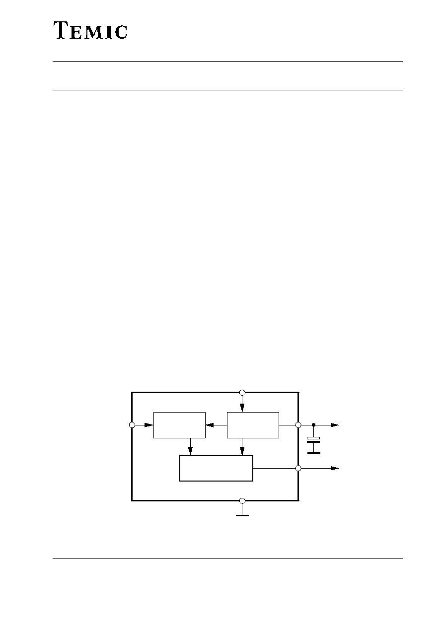
Block diagram
Log RSSI /
AM demodulator
IF ≠ amplifier
Bandgap
V
Ref
internal
8
V
S
8
V
Ref
C
Ref
4
log RSSI
log AM
out
1, 2, 3, 6
GND
5
IF
in
95 10215
Figure 1. Block diagram
TELEFUNKEN Semiconductors
U4314B
Rev. A1: 26.06.1995
2 (7)
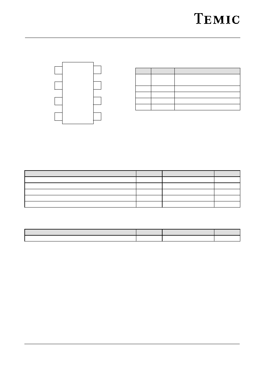
Pin Description
1
2
3
4
8
7
6
5
95 10461
GND
GND
GND
AM
out
V
S
V
Ref
GND
IF
in
Figure 2. Pin description
Pin
Symbol
Function
1, 2,
3, 6
GND
Ground
4
AM
out
RSSI / AM current output
5
IF
in
IF input
7
V
Ref
Reference voltage
8
V
S
Supply voltage
Absolute Maximum Ratings
Parameters
Symbol
Value
Unit
Supply voltage
V
S
13
V
Power dissipation at T
amb
= 85
∞
C
P
tot
220
mW
Junction temperature
T
j
125
∞
C
Ambient temperature
T
amb
≠40 to +85
∞
C
Storage temperature
T
stg
≠55 to +125
∞
C
Thermal Resistance
Parameters
Symbol
Value
Unit
Junction ambient
R
thJA
180
K/W
TELEFUNKEN Semiconductors
U4314B
Rev. A1: 26.06.1995
3 (7)
Electrical Characteristics
V
S
= 5 V, T
amb
= 25
∞
C, f
in
= 10.7 MHz unless otherwise specified. Test circuit see figure 8. IF voltage levels are referred
to the input of the matching network and therefore approximately 5.6 dB higher than referred to Pin 5.
Parameters
Test Conditions / Pins
Symbol
Min.
Typ.
Max.
Unit
Characteristics
Supply voltage range
Pin 8
V
S
3
12
V
Supply current
Pin 8
I
S
0.8
1.25
mA
Bandgap
Regulated voltage (without
external load)
Pin 7
V
ref
2.3
2.4
2.5
V
Source resistance
Pin 7
R
ref
2
5
W
Output current
Pin 7
I
ref
5
mA
External capacitor
Pin 7
C
ref
4.7
mF
Power supply rejection
ratio
f = 50 Hz
Pin 7
psrr
60
dB
IF amplifier
Input resistance
Pin 5
R
in
200
330
650
W
Input capacitance
Pin 5
C
in
5
pF
≠3 dB limiting point
Pin 5
V
IFin
26
36
46
dB
mV
Maximum AM input
voltage
Pin 5
V
IFinmax
96
dB
mV
AM
out
quiescent current
R
load
= 10 k
W
Pin 4
I
AMout
10
22
38
mA
Maximum AM
out
current
V
IFin
= 96 dB
mV,
R
load
= 10 k
W
Pin 4
I
AMoutmax
75
105
125
mA
Circuit Description
General functions
The integrated circuit U4314B includes the following
functions: IF-amplifier, logarithmic RSSI / AM demodu-
lator and voltage-regulator.
The 10.7 MHz IF-signal from the front end passes the in-
tegrated IF-amplifier which operates to a logarithmic
RSSI
/
AM-demodulator. A logarithmic demodulator
was implemented to avoid settling time problems ef-
fected by use of an AGC. The temperature compensated
reference voltage of 2.4 V is externally available. The
value of the external blocking capacitor can be adapted to
the maximum expected load current out of the voltage
regulator. The total supply current is typically 0.8 mA
plus this load current.
95 10216
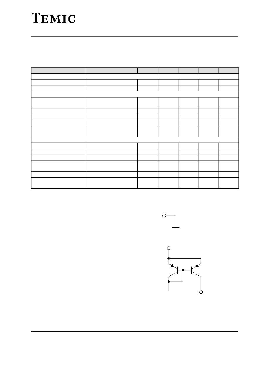
1, 2, 3, 6
Figure 3. Pin 1, 2, 3, 6 GND
7
95 10219
4
Figure 4. Pin 4 AM
out
TELEFUNKEN Semiconductors
U4314B
Rev. A1: 26.06.1995
4 (7)
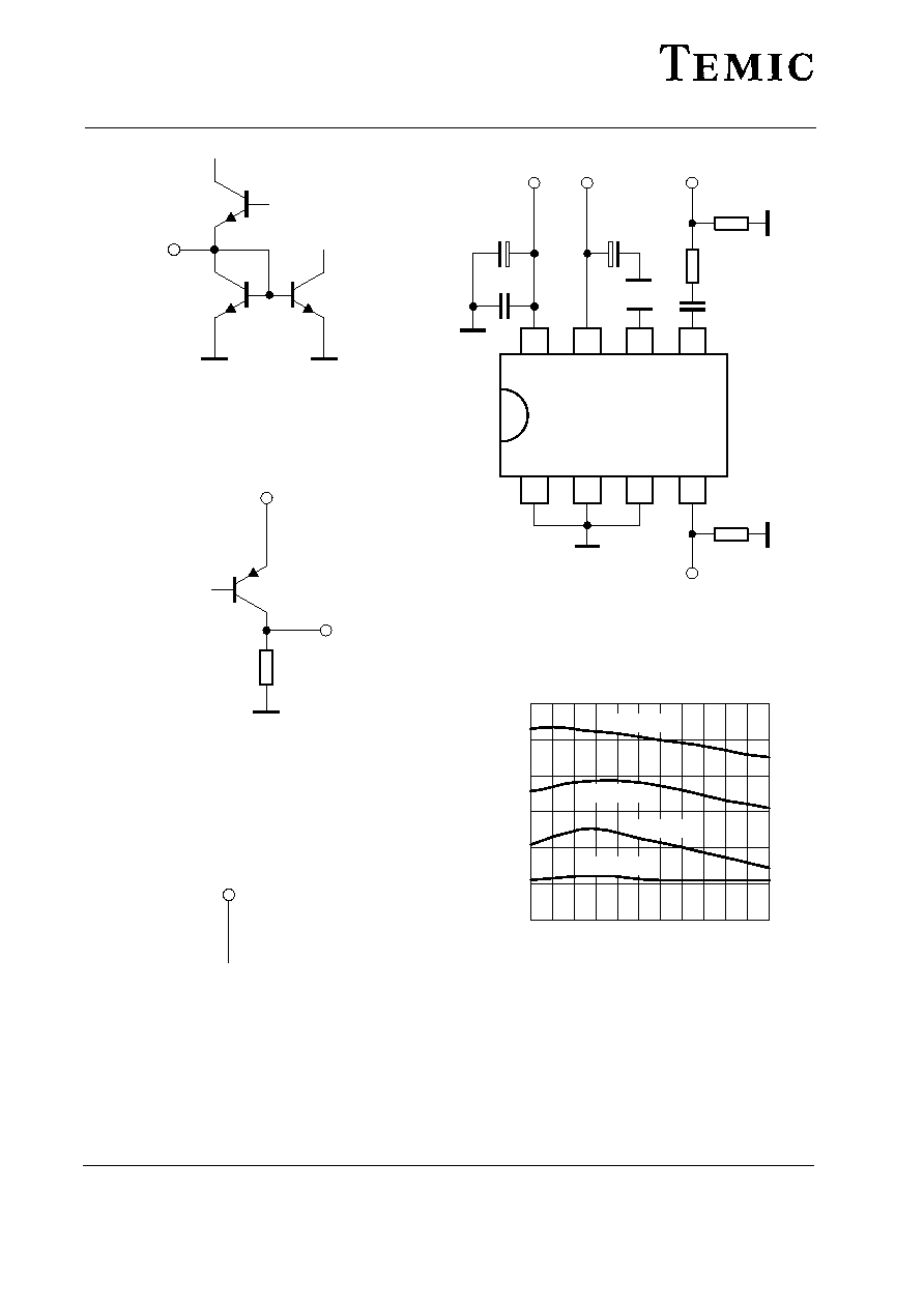
95 10220
5
Figure 5. Pin 5 IF
in
7
95 10222
8
Figure 6. Pin 7 V
Ref
95 10223
8
Figure 7. Pin 8 V
S
8
7
6
5
1
2
3
4
U4314B
100 nF
4.7
mF
4.7
mF
C
Ref
=
V
Ref
V
S
IF
in
56
W
300
W
10 nF
R
load
=
10 k
W
RSSI / AM
out
95 10224
Figure 8. Test circuit
5
7
9
11
13
IF≠Frequency ( MHz)
16
95 10463
15
12
14
6
8
10
0
20
40
60
80
120
AM Output Current (
A
)
100
m
90 dB
mV
70 dB
mV
50 dB
mV
30 dB
mV
Figure 9. IF-Frequency response

TELEFUNKEN Semiconductors
U4314B
Rev. A1: 26.06.1995
5 (7)
10
30
50
70
90
0
20
40
60
80
120
AM Output Current (
A
)
IF≠Input Level ( dB
mV )
110
95 10462
100
+85
∞
C
+25
∞
C
≠40
∞
C
m
Figure 10. AM-demodulator characteristic (f
in
= 10.7 MHz)
0
20
40
60
80
0
10
20
30
40
70
AM Output Current (
A
)
IF≠Input Level ( dB
mV )
100
95 10335
m
50
60
Figure 11. IAM
out
of U4314B in the application circuit of
figure 12 (f
in
= 107 MHz)
The following circuit is a mere proposal, how to improve
sensitivity and extend the dynamic range of U4314B to
more than 90 dB. However in most applications the basic
dynamic range of more than 60 dB is sufficient. TEMIC
TELEFUNKEN microelectronic GmbH makes no repre-
sentation that the use of this circuit will not refringe on
existing or future patents and no responsibility for the use
of the information contained herein is assumed. This
circuit is neither optimized concerning tolerances of the
components nor tested versus temperature. It should work
with a single supply voltage of 3 to 12 V. A npn transistor
array CA3045 or similar is used. At least four transistors
are needed to realize two current mirrors and the fifth acts
as a preamplifier. The variable resistor P
1
is used to com-
pensate the quiescent current of the logarithmic
demodulator output and may be replaced by a fixed resis-
tor (typ. 3.3 k
W). The total supply current depends on the
IF-input level and varies between 2 and 7 mA. It is mainly
determined by the current through the PIN diode. We
recommend to use the BA679S PIN diode available from
TEMIC TELEFUNKEN microelectronic GmbH. The
input impedance of this application circuit is approxi-
mately 1.5 k
W || 13 pF.