 | –≠–ª–µ–∫—Ç—Ä–æ–Ω–Ω—ã–π –∫–æ–º–ø–æ–Ω–µ–Ω—Ç: U4460BG | –°–∫–∞—á–∞—Ç—å:  PDF PDF  ZIP ZIP |
TELEFUNKEN Semiconductors
U4460BG
Preliminary Information
Rev. A1: 15.08.1995
1 (9)
Video IF Amplifier with FPLL Demodulation
Description
The U 4460 BG is an integrated bipolar circuit for video
IF (VIF) signal processing in TV/VCR and multimedia
applications.
The circuit processes all TV video IF signals with
negative modulation (e.g. B/G standard).
Features
D
Active carrier generation by FPLL principle
(frequency≠phase≠locked≠loop) for true
synchronous demodulation
D
Very linear video demodulation, good pulse
response and excellent intermodulation figures
D
VCO is operating on picture carrier frequency
D Alignment≠free AFC, no external reference circuit
D VIF≠AGC with peak sync detection
D Tuner AGC with adjustable take over point
D
5V supply voltage; low power consumption
D
Relevant pinning is compatible with the
TDA 4474 /71 video≠/sound IF combination
Package:
28 pin shrink≠dual≠inline≠plastic (SDIP28)
œœ
œœ
œ
œ
œœ
œœ
œœ
AGC
(VIF)
Tuner
AGC
œœ
œœ
œœ
œœ
œœ
œœ
œœ
œœ
12
11
Tuner
VCO
+
phase shift
AFC
Supply
œœ
œœ
œœ
VCO
21
22
19
Loop
filter
œœ
œœ
Offset
comp.
(optional)
27
FPLL
0
∞
90
∞
VIF amp
5
6
7
VIF
C
AGC
Take over point
23
13
3,8,17
24
V
S
œ
œ
18
C
Ref
AFC
Video
œœ
œœ
Video det.
œœ
20
AFC
switch
œ
95 9815
œœ
œœ
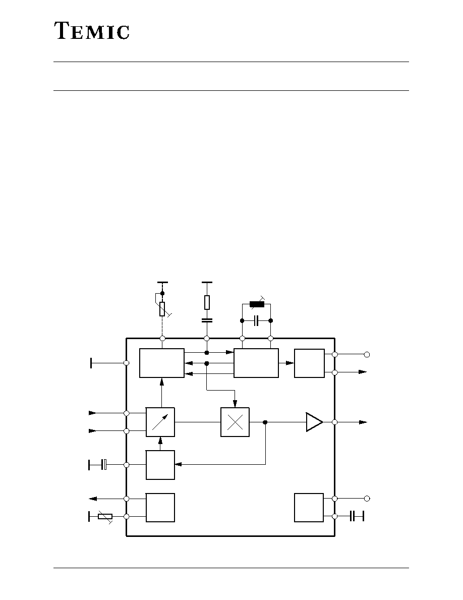
Figure 1. Block diagram
TELEFUNKEN Semiconductors
U4460BG
Preliminary Information
Rev. A1: 15.08.1995
2 (9)
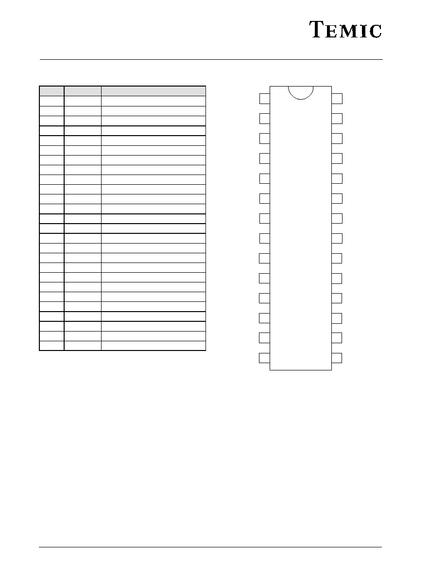
Pin description
Pin
Symbol
Function
¡¡¡
¡¡¡
1
¡¡¡¡¡
¡¡¡¡¡
n.c.
¡¡¡¡¡¡¡¡¡¡
¡¡¡¡¡¡¡¡¡¡
not connected
¡¡¡
¡¡¡
2
¡¡¡¡¡
¡¡¡¡¡
n.c.
¡¡¡¡¡¡¡¡¡¡
¡¡¡¡¡¡¡¡¡¡
not connected
¡¡¡
¡¡¡
3
¡¡¡¡¡
¡¡¡¡¡
GND
¡¡¡¡¡¡¡¡¡¡
¡¡¡¡¡¡¡¡¡¡
Ground
¡¡¡
¡¡¡
4
¡¡¡¡¡
¡¡¡¡¡
n.c.
¡¡¡¡¡¡¡¡¡¡
¡¡¡¡¡¡¡¡¡¡
not connected
¡¡¡
5, 6
¡¡¡¡¡
V
i,VIF
¡¡¡¡¡¡¡¡¡¡
VIF input (symmetrical)
¡¡¡
¡¡¡
7
¡¡¡¡¡
¡¡¡¡¡
C
AGC
¡¡¡¡¡¡¡¡¡¡
¡¡¡¡¡¡¡¡¡¡
VIF≠AGC (time constant)
¡¡¡
¡¡¡
8
¡¡¡¡¡
¡¡¡¡¡
GND
¡¡¡¡¡¡¡¡¡¡
¡¡¡¡¡¡¡¡¡¡
Ground
¡¡¡
¡¡¡
9
¡¡¡¡¡
¡¡¡¡¡
n.c.
¡¡¡¡¡¡¡¡¡¡
¡¡¡¡¡¡¡¡¡¡
not connected
¡¡¡
¡¡¡
10
¡¡¡¡¡
¡¡¡¡¡
n.c.
¡¡¡¡¡¡¡¡¡¡
¡¡¡¡¡¡¡¡¡¡
not connected
¡¡¡
¡¡¡
11
¡¡¡¡¡
¡¡¡¡¡
R
top
¡¡¡¡¡¡¡¡¡¡
¡¡¡¡¡¡¡¡¡¡
Take over point, tuner AGC
¡¡¡
¡¡¡
12
¡¡¡¡¡
¡¡¡¡¡
I
tun
¡¡¡¡¡¡¡¡¡¡
¡¡¡¡¡¡¡¡¡¡
Tuner AGC output current
¡¡¡
¡¡¡
13
¡¡¡¡¡
¡¡¡¡¡
V
o,vid
¡¡¡¡¡¡¡¡¡¡
¡¡¡¡¡¡¡¡¡¡
Video output
¡¡¡
14
¡¡¡¡¡
n.c.
¡¡¡¡¡¡¡¡¡¡
not connected
¡¡¡
¡¡¡
15
¡¡¡¡¡
¡¡¡¡¡
n.c.
¡¡¡¡¡¡¡¡¡¡
¡¡¡¡¡¡¡¡¡¡
not connected
¡¡¡
¡¡¡
16
¡¡¡¡¡
¡¡¡¡¡
n.c.
¡¡¡¡¡¡¡¡¡¡
¡¡¡¡¡¡¡¡¡¡
not connected
¡¡¡
¡¡¡
17
¡¡¡¡¡
¡¡¡¡¡
GND
¡¡¡¡¡¡¡¡¡¡
¡¡¡¡¡¡¡¡¡¡
Ground
¡¡¡
¡¡¡
18
¡¡¡¡¡
¡¡¡¡¡
C
ref
¡¡¡¡¡¡¡¡¡¡
¡¡¡¡¡¡¡¡¡¡
Internal reference voltage
¡¡¡
¡¡¡
19
¡¡¡¡¡
¡¡¡¡¡
LF
¡¡¡¡¡¡¡¡¡¡
¡¡¡¡¡¡¡¡¡¡
Loop filter
¡¡¡
¡¡¡
20
¡¡¡¡¡
¡¡¡¡¡
n.c.
¡¡¡¡¡¡¡¡¡¡
¡¡¡¡¡¡¡¡¡¡
AFC switch
¡¡¡
¡¡¡
21, 22
¡¡¡¡¡
¡¡¡¡¡
V
vco
¡¡¡¡¡¡¡¡¡¡
¡¡¡¡¡¡¡¡¡¡
VCO circuit
¡¡¡
23
¡¡¡¡¡
V
AFC
¡¡¡¡¡¡¡¡¡¡
AFC output
¡¡¡
¡¡¡
24
¡¡¡¡¡
¡¡¡¡¡
V
s
¡¡¡¡¡¡¡¡¡¡
¡¡¡¡¡¡¡¡¡¡
Supply voltage
¡¡¡
¡¡¡
25
¡¡¡¡¡
¡¡¡¡¡
n.c.
¡¡¡¡¡¡¡¡¡¡
¡¡¡¡¡¡¡¡¡¡
not connected
¡¡¡
¡¡¡
26
¡¡¡¡¡
¡¡¡¡¡
n.c.
¡¡¡¡¡¡¡¡¡¡
¡¡¡¡¡¡¡¡¡¡
not connected
¡¡¡
¡¡¡
27
¡¡¡¡¡
¡¡¡¡¡
R
comp
¡¡¡¡¡¡¡¡¡¡
¡¡¡¡¡¡¡¡¡¡
Offset compensation
¡¡¡
¡¡¡
28
¡¡¡¡¡
¡¡¡¡¡
n.c.
¡¡¡¡¡¡¡¡¡¡
¡¡¡¡¡¡¡¡¡¡
not connected
1
2
3
4
5
6
7
8
10
9
27
22
21
20
18
19
17
12
11
28
25
26
23
24
V
i
, VIF
C
AGC
GND
n.c.
n.c.
R
top
n.c.
V
i
, VIF
I
tun
GND
n.c.
n.c.
V
AFC
V
VCO
V
VCO
n.c.
LF
C
Ref
n.c.
V
S
GND
n.c.
R
comp
n.c.
16
15
14
13
95 10650
V
O
, vid
n.c.
n.c.
n.c.
U4460BG
Figure 2. Pin configuration
Circuit description
Vision IF amplifier
The video IF signal (VIF) is fed through a SAW filter to
the VIF input (Pin 5≠6). The VIF amplifier consists of
three AC≠coupled amplifier stages. Each differential
amplifier is gain controlled by the automatic gain control
(VIF≠AGC). Output signal of the VIF amplifier is applied
to the FPLL carrier generation and the video
demodulator.
VIF≠AGC and adjustable tuner AGC
At Pin 7 the VIF≠AGC charges/discharges the AGC
capacitor to generate a control voltage for setting gain of
VIF amplifier and tuner in order to keep the video output
signal at a constant level. Therefore the sync level of the
demodulated video signal is the criterion for a fast charge/
discharge of the AGC capacitor.
The control voltage (AGC voltage at Pin 7) is transferred
to an internal control signal and fed to the tuner AGC to
generate the tuner AGC current at Pin 12 (open collector
output). Take over point of the tuner AGC can be adjusted
at Pin 11 by a potentiometer or an external DC voltage
(from interface circuit or microprocessor).

TELEFUNKEN Semiconductors
U4460BG
Preliminary Information
Rev. A1: 15.08.1995
3 (9)
FPLL, VCO and AFC
The FPLL circuit (frequency phase locked loop) consists
of a frequency and phase detector to generate control
voltage for the VCO tuning. In the locked mode the VCO
is controlled by the phase detector and in unlocked mode
the frequency detector is superimposed. The VCO
operates with an external resonance circuit (L and C par-
allel) and is controlled by internal varicaps. The VCO
control voltage is also converted to a current and
represents the AFC output signal at Pin 23.
A practicable VCO alignment of the external coil is the
adjustment to zero AFC output current at Pin 23. At centre
frequency the AFC output current is equal to zero. The
optional potentiometer at Pin 27 allows an offset
compensation of the VCO phase for improved sound
quality (fine adjustment). Without a potentiometer (open
circuit at Pin 27) this offset compensation is not active.
The oscillator signal passes a phase shifter and supplies
the in≠phase signal (0) and the quadrature signal (90) of
the generated picture carrier.
Video demodulation and amplifier
The video IF signal, which is applied from the gain
controlled IF amplifier, is multiplied with the inphase
component of the VCO signal. The video demodulator is
designed for low distortion and large bandwidth. The
demodulator output signal passes an integrated low pass
filter for attenuation of the residual vision carrier and is
fed to the video amplifier. The video amplifier is realized
by an operational amplifier with internal feedback and 8
MHz bandwidth (≠3dB). The video signal is fed to VIF≠
AGC and to the video output buffer. This amplifier with
6dB gain offers easy adaption of the sound trap. For
nominal video IF modulation the video output signal at
Pin 13 is 2 V (peak to peak value).
Internal voltage stabilizer
The internal bandgap reference ensures constant
performance independant of supply voltage and
temperature.
Absolute maximum values
Reference point pin 3 (8, 17), unless otherwise specified
Parameters
Symbol
Value
Unit
¡¡¡¡¡¡¡¡¡¡¡¡¡¡¡¡¡
¡¡¡¡¡¡¡¡¡¡¡¡¡¡¡¡¡
Supply voltage
Pin 24
¡¡¡¡¡
¡¡¡¡¡
V
s
¡¡¡¡¡¡¡¡
¡¡¡¡¡¡¡¡
9.0
¡¡¡¡¡
¡¡¡¡¡
V
¡¡¡¡¡¡¡¡¡¡¡¡¡¡¡¡¡
¡¡¡¡¡¡¡¡¡¡¡¡¡¡¡¡¡
Supply current
Pin 24
¡¡¡¡¡
¡¡¡¡¡
I
s
¡¡¡¡¡¡¡¡
¡¡¡¡¡¡¡¡
85
¡¡¡¡¡
¡¡¡¡¡
mA
¡¡¡¡¡¡¡¡¡¡¡¡¡¡¡¡¡
¡¡¡¡¡¡¡¡¡¡¡¡¡¡¡¡¡
Power dissipation, V
s
= + 9 V
¡¡¡¡¡
¡¡¡¡¡
P
¡¡¡¡¡¡¡¡
¡¡¡¡¡¡¡¡
765
¡¡¡¡¡
¡¡¡¡¡
mW
¡¡¡¡¡¡¡¡¡¡¡¡¡¡¡¡¡
¡¡¡¡¡¡¡¡¡¡¡¡¡¡¡¡¡
Output currents
Pin 13
¡¡¡¡¡
¡¡¡¡¡
I
out
¡¡¡¡¡¡¡¡
¡¡¡¡¡¡¡¡
5
¡¡¡¡¡
¡¡¡¡¡
mA
¡¡¡¡¡¡¡¡¡¡¡¡¡¡¡¡¡
¡¡¡¡¡¡¡¡¡¡¡¡¡¡¡¡¡
External voltages
Pin 5, 6, 7, 11, 13, 18,
19, 27
¡¡¡¡¡
¡¡¡¡¡
V
ext
¡¡¡¡¡¡¡¡
¡¡¡¡¡¡¡¡
+ 4.5
¡¡¡¡¡
¡¡¡¡¡
V
¡¡¡¡¡¡¡¡¡¡¡¡¡¡¡¡¡
¡¡¡¡¡¡¡¡¡¡¡¡¡¡¡¡¡
Pin 20,21
¡¡¡¡¡
¡¡¡¡¡
¡¡¡¡¡¡¡¡
¡¡¡¡¡¡¡¡
+ 3.5
¡¡¡¡¡
¡¡¡¡¡
V
¡¡¡¡¡¡¡¡¡¡¡¡¡¡¡¡¡
¡¡¡¡¡¡¡¡¡¡¡¡¡¡¡¡¡
Pin 12
¡¡¡¡¡
¡¡¡¡¡
¡¡¡¡¡¡¡¡
¡¡¡¡¡¡¡¡
+ 13.5
¡¡¡¡¡
¡¡¡¡¡
V
¡¡¡¡¡¡¡¡¡¡¡¡¡¡¡¡¡
¡¡¡¡¡¡¡¡¡¡¡¡¡¡¡¡¡
Pin 20,23
¡¡¡¡¡
¡¡¡¡¡
¡¡¡¡¡¡¡¡
¡¡¡¡¡¡¡¡
V
s
¡¡¡¡¡
¡¡¡¡¡
V
¡¡¡¡¡¡¡¡¡¡¡¡¡¡¡¡¡
¡¡¡¡¡¡¡¡¡¡¡¡¡¡¡¡¡
Junction temperature
¡¡¡¡¡
¡¡¡¡¡
T
junc
¡¡¡¡¡¡¡¡
¡¡¡¡¡¡¡¡
+125
¡¡¡¡¡
¡¡¡¡¡
∞
C
¡¡¡¡¡¡¡¡¡¡¡¡¡¡¡¡¡
¡¡¡¡¡¡¡¡¡¡¡¡¡¡¡¡¡
Storage temperature
¡¡¡¡¡
¡¡¡¡¡
T
stor
¡¡¡¡¡¡¡¡
¡¡¡¡¡¡¡¡
≠25 to +125
¡¡¡¡¡
¡¡¡¡¡
∞
C
¡¡¡¡¡¡¡¡¡¡¡¡¡¡¡¡¡
¡¡¡¡¡¡¡¡¡¡¡¡¡¡¡¡¡
Electrostatic handling *)
all pins
¡¡¡¡¡
¡¡¡¡¡
V
ESD
¡¡¡¡¡¡¡¡
¡¡¡¡¡¡¡¡
t.b.f.
¡¡¡¡¡
¡¡¡¡¡
V
*) Equivalent to discharging a 200 pF capacitor through a 0 resistor
Operating range
Parameters
Symbol
Value
Unit
¡¡¡¡¡¡¡¡¡¡¡¡¡¡¡¡¡
¡¡¡¡¡¡¡¡¡¡¡¡¡¡¡¡¡
Supply voltage range
Pin25
¡¡¡¡¡
¡¡¡¡¡
V
s
¡¡¡¡¡¡¡¡
¡¡¡¡¡¡¡¡
4.5 to 9.0
¡¡¡¡¡
¡¡¡¡¡
V
¡¡¡¡¡¡¡¡¡¡¡¡¡¡¡¡¡
¡¡¡¡¡¡¡¡¡¡¡¡¡¡¡¡¡
Ambient temperature
¡¡¡¡¡
¡¡¡¡¡
T
amb
¡¡¡¡¡¡¡¡
¡¡¡¡¡¡¡¡
0 to +85
¡¡¡¡¡
¡¡¡¡¡
∞
C

TELEFUNKEN Semiconductors
U4460BG
Preliminary Information
Rev. A1: 15.08.1995
4 (9)
Thermal resistance
Parameters
Symbol
Value
Unit
¡¡¡¡¡¡¡¡¡¡¡¡¡¡¡¡¡
¡
¡¡¡¡¡¡¡¡¡¡¡¡¡¡¡
¡
¡¡¡¡¡¡¡¡¡¡¡¡¡¡¡¡¡
Thermal resistance:
junction≠ambient when soldered to PCB
¡¡¡¡¡
¡
¡¡¡
¡
¡¡¡¡¡
R
thja
¡¡¡¡¡¡¡¡
¡
¡¡¡¡¡¡
¡
¡¡¡¡¡¡¡¡
55
¡¡¡¡¡
¡
¡¡¡
¡
¡¡¡¡¡
K/W
Electrical Characteristics
V
s
= +5V, T
amb
= +25
∞
C; reference point pin 3 (8, 17), unless otherwise specified
Parameters
Test Conditions / Pins
Symbol
Min.
Typ.
Max.
Unit
¡¡¡¡¡¡¡¡¡¡¡¡¡¡¡¡¡¡¡¡¡¡¡¡¡¡¡¡¡¡¡¡
¡¡¡¡¡¡¡¡¡¡¡¡¡¡¡¡¡¡¡¡¡¡¡¡¡¡¡¡¡¡¡¡
DC≠supply:
Pin 24
¡¡¡¡¡¡¡¡¡
¡¡¡¡¡¡¡¡¡
Supply voltage
¡¡¡¡¡¡¡¡¡
¡¡¡¡¡¡¡¡¡
¡¡¡¡
¡¡¡¡
V
s
¡¡¡¡
¡¡¡¡
4.5
¡¡¡¡
¡¡¡¡
5.0
¡¡¡¡
¡¡¡¡
9.0
¡¡¡¡
¡¡¡¡
V
¡¡¡¡¡¡¡¡¡
¡¡¡¡¡¡¡¡¡
Supply current:
¡¡¡¡¡¡¡¡¡
¡¡¡¡¡¡¡¡¡
¡¡¡¡
¡¡¡¡
I
s
¡¡¡¡
¡¡¡¡
¡¡¡¡
¡¡¡¡
75
¡¡¡¡
¡¡¡¡
85
¡¡¡¡
¡¡¡¡
mA
¡¡¡¡¡¡¡¡¡¡¡¡¡¡¡¡¡¡¡¡¡¡¡¡¡¡¡¡¡¡¡¡
¡¡¡¡¡¡¡¡¡¡¡¡¡¡¡¡¡¡¡¡¡¡¡¡¡¡¡¡¡¡¡¡
VIF≠input:
Pins 5≠6
¡¡¡¡¡¡¡¡¡
¡
¡¡¡¡¡¡¡
¡
¡¡¡¡¡¡¡¡¡
Input sensitivity, RMS
value
¡¡¡¡¡¡¡¡¡
¡
¡¡¡¡¡¡¡
¡
¡¡¡¡¡¡¡¡¡
for FPLL locked
¡¡¡¡
¡
¡¡
¡
¡¡¡¡
v
in
¡¡¡¡
¡
¡¡
¡
¡¡¡¡
¡¡¡¡
¡
¡¡
¡
¡¡¡¡
80
¡¡¡¡
¡
¡¡
¡
¡¡¡¡
120
¡¡¡¡
¡
¡¡
¡
¡¡¡¡
µ
V
¡¡¡¡¡¡¡¡¡
¡¡¡¡¡¡¡¡¡
Input impedance
¡¡¡¡¡¡¡¡¡
¡¡¡¡¡¡¡¡¡
see note 1
¡¡¡¡
¡¡¡¡
R
in
¡¡¡¡
¡¡¡¡
¡¡¡¡
¡¡¡¡
1.2
¡¡¡¡
¡¡¡¡
¡¡¡¡
¡¡¡¡
k
¡¡¡¡¡¡¡¡¡
¡¡¡¡¡¡¡¡¡
Input capacitance
¡¡¡¡¡¡¡¡¡
¡¡¡¡¡¡¡¡¡
see note 1
¡¡¡¡
¡¡¡¡
C
in
¡¡¡¡
¡¡¡¡
¡¡¡¡
¡¡¡¡
2
¡¡¡¡
¡¡¡¡
¡¡¡¡
¡¡¡¡
pF
¡¡¡¡¡¡¡¡¡¡¡¡¡¡¡¡¡¡¡¡¡¡¡¡¡¡¡¡¡¡¡¡
¡¡¡¡¡¡¡¡¡¡¡¡¡¡¡¡¡¡¡¡¡¡¡¡¡¡¡¡¡¡¡¡
VIF≠AGC:
Pin 7
¡¡¡¡¡¡¡¡¡
¡¡¡¡¡¡¡¡¡
IF gain control range
¡¡¡¡¡¡¡¡¡
¡¡¡¡¡¡¡¡¡
¡¡¡¡
¡¡¡¡
G
v
¡¡¡¡
¡¡¡¡
60
¡¡¡¡
¡¡¡¡
65
¡¡¡¡
¡¡¡¡
¡¡¡¡
¡¡¡¡
dB
¡¡¡¡¡¡¡¡¡
¡¡¡¡¡¡¡¡¡
AGC capacitor
¡¡¡¡¡¡¡¡¡
¡¡¡¡¡¡¡¡¡
¡¡¡¡
¡¡¡¡
C
AGC
¡¡¡¡
¡¡¡¡
¡¡¡¡
¡¡¡¡
2.2
¡¡¡¡
¡¡¡¡
¡¡¡¡
¡¡¡¡
µ
F
¡¡¡¡¡¡¡¡¡
¡
¡¡¡¡¡¡¡
¡
¡¡¡¡¡¡¡¡¡
Switching voltage: VCR
mode
¡¡¡¡¡¡¡¡¡
¡
¡¡¡¡¡¡¡
¡
¡¡¡¡¡¡¡¡¡
see note 2
¡¡¡¡
¡
¡¡
¡
¡¡¡¡
V
sw
¡¡¡¡
¡
¡¡
¡
¡¡¡¡
¡¡¡¡
¡
¡¡
¡
¡¡¡¡
4.0
¡¡¡¡
¡
¡¡
¡
¡¡¡¡
¡¡¡¡
¡
¡¡
¡
¡¡¡¡
V
¡¡¡¡¡¡¡¡¡
¡
¡¡¡¡¡¡¡
¡
¡¡¡¡¡¡¡¡¡
Switching current: VCR
mode
¡¡¡¡¡¡¡¡¡
¡
¡¡¡¡¡¡¡
¡
¡¡¡¡¡¡¡¡¡
see note 2
¡¡¡¡
¡
¡¡
¡
¡¡¡¡
I
sw
¡¡¡¡
¡
¡¡
¡
¡¡¡¡
¡¡¡¡
¡
¡¡
¡
¡¡¡¡
50
¡¡¡¡
¡
¡¡
¡
¡¡¡¡
¡¡¡¡
¡
¡¡
¡
¡¡¡¡
A
¡¡¡¡¡¡¡¡¡¡¡¡¡¡¡¡¡¡¡¡¡¡¡¡¡¡¡¡¡¡¡¡
¡¡¡¡¡¡¡¡¡¡¡¡¡¡¡¡¡¡¡¡¡¡¡¡¡¡¡¡¡¡¡¡
Tuner≠AGC:
Pins 11, 12 see note 3
¡¡¡¡¡¡¡¡¡
¡
¡¡¡¡¡¡¡
¡
¡¡¡¡¡¡¡¡¡
Available tuner≠AGC cur-
rent
¡¡¡¡¡¡¡¡¡
¡
¡¡¡¡¡¡¡
¡
¡¡¡¡¡¡¡¡¡
¡¡¡¡
¡
¡¡
¡
¡¡¡¡
I
tun
¡¡¡¡
¡
¡¡
¡
¡¡¡¡
1
¡¡¡¡
¡
¡¡
¡
¡¡¡¡
2
¡¡¡¡
¡
¡¡
¡
¡¡¡¡
4
¡¡¡¡
¡
¡¡
¡
¡¡¡¡
mA
¡¡¡¡¡¡¡¡¡
¡¡¡¡¡¡¡¡¡
Allowable output voltage
¡¡¡¡¡¡¡¡¡
¡¡¡¡¡¡¡¡¡
¡¡¡¡
¡¡¡¡
V
out
¡¡¡¡
¡¡¡¡
0.3
¡¡¡¡
¡¡¡¡
¡¡¡¡
¡¡¡¡
13.5
¡¡¡¡
¡¡¡¡
V
¡¡¡¡¡¡¡¡¡
¡
¡¡¡¡¡¡¡
¡
¡¡¡¡¡¡¡¡¡
IF slip ≠ tuner AGC
¡¡¡¡¡¡¡¡¡
¡
¡¡¡¡¡¡¡
¡
¡¡¡¡¡¡¡¡¡
current I
tun
:
10% to 90%
¡¡¡¡
¡
¡¡
¡
¡¡¡¡
G
IF
¡¡¡¡
¡
¡¡
¡
¡¡¡¡
¡¡¡¡
¡
¡¡
¡
¡¡¡¡
8
¡¡¡¡
¡
¡¡
¡
¡¡¡¡
10
¡¡¡¡
¡
¡¡
¡
¡¡¡¡
dB
¡¡¡¡¡¡¡¡¡
¡
¡¡¡¡¡¡¡
¡
¡
¡¡¡¡¡¡¡
¡
¡¡¡¡¡¡¡¡¡
IF input signal for mini-
mum
take over point
¡¡¡¡¡¡¡¡¡
¡
¡¡¡¡¡¡¡
¡
¡
¡¡¡¡¡¡¡
¡
¡¡¡¡¡¡¡¡¡
R
top
= 10 k
(V
top
= 4.5 V)
¡¡¡¡
¡
¡¡
¡
¡
¡¡
¡
¡¡¡¡
v
in
¡¡¡¡
¡
¡¡
¡
¡
¡¡
¡
¡¡¡¡
¡¡¡¡
¡
¡¡
¡
¡
¡¡
¡
¡¡¡¡
¡¡¡¡
¡
¡¡
¡
¡
¡¡
¡
¡¡¡¡
4
¡¡¡¡
¡
¡¡
¡
¡
¡¡
¡
¡¡¡¡
mV
¡¡¡¡¡¡¡¡¡
¡
¡¡¡¡¡¡¡
¡
¡¡¡¡¡¡¡¡¡
IF input signal for maxi-
mum
take over point
¡¡¡¡¡¡¡¡¡
¡
¡¡¡¡¡¡¡
¡
¡¡¡¡¡¡¡¡¡
R
top
= 0
(V
top =
0.8 V)
¡¡¡¡
¡
¡¡
¡
¡¡¡¡
v
in
¡¡¡¡
¡
¡¡
¡
¡¡¡¡
40
¡¡¡¡
¡
¡¡
¡
¡¡¡¡
¡¡¡¡
¡
¡¡
¡
¡¡¡¡
¡¡¡¡
¡
¡¡
¡
¡¡¡¡
mV
¡¡¡¡¡¡¡¡¡
¡
¡¡¡¡¡¡¡
¡
¡
¡¡¡¡¡¡¡
¡
¡¡¡¡¡¡¡¡¡
Variation of the take over
point
by temperature
¡¡¡¡¡¡¡¡¡
¡
¡¡¡¡¡¡¡
¡
¡
¡¡¡¡¡¡¡
¡
¡¡¡¡¡¡¡¡¡
T
amb
= 55
∞
C
VIF≠AGC: G
v
= 46 dB
¡¡¡¡
¡
¡¡
¡
¡
¡¡
¡
¡¡¡¡
v
in
¡¡¡¡
¡
¡¡
¡
¡
¡¡
¡
¡¡¡¡
¡¡¡¡
¡
¡¡
¡
¡
¡¡
¡
¡¡¡¡
2
¡¡¡¡
¡
¡¡
¡
¡
¡¡
¡
¡¡¡¡
3
¡¡¡¡
¡
¡¡
¡
¡
¡¡
¡
¡¡¡¡
dB
¡¡¡¡¡¡¡¡¡¡¡¡¡¡¡¡¡¡¡¡¡¡¡¡¡¡¡¡¡¡¡¡
FPLL and VCO:
Pins 19, 21, 22, 27
¡¡¡¡¡¡¡¡¡
¡¡¡¡¡¡¡¡¡
Max. oscillator frequency
¡¡¡¡¡¡¡¡¡
¡¡¡¡¡¡¡¡¡
for carrier generation
¡¡¡¡
¡¡¡¡
f
vco
¡¡¡¡
¡¡¡¡
70
¡¡¡¡
¡¡¡¡
¡¡¡¡
¡¡¡¡
¡¡¡¡
¡¡¡¡
MHz
¡¡¡¡¡¡¡¡¡
¡
¡¡¡¡¡¡¡
¡
¡¡¡¡¡¡¡¡¡
Vision carrier capture range
¡¡¡¡¡¡¡¡¡
¡
¡¡¡¡¡¡¡
¡
¡¡¡¡¡¡¡¡¡
f
vco
= 38.9 MHz
C
vco
= 6.8 pF
¡¡¡¡
¡
¡¡
¡
¡¡¡¡
f
cap
¡¡¡¡
¡
¡¡
¡
¡¡¡¡
1.5
¡¡¡¡
¡
¡¡
¡
¡¡¡¡
2
¡¡¡¡
¡
¡¡
¡
¡¡¡¡
¡¡¡¡
¡
¡¡
¡
¡¡¡¡
MHz
¡¡¡¡¡¡¡¡¡
¡
¡¡¡¡¡¡¡
¡
¡
¡¡¡¡¡¡¡
¡
¡¡¡¡¡¡¡¡¡
Oscillator drift (free run-
ing) as function of temper-
ature
¡¡¡¡¡¡¡¡¡
¡
¡¡¡¡¡¡¡
¡
¡
¡¡¡¡¡¡¡
¡
¡¡¡¡¡¡¡¡¡
see note 4
T
amb
= 55
∞
C,
C
vco
= 6.8 pF,
f
vco
= 38.9 MHz
¡¡¡¡
¡
¡¡
¡
¡
¡¡
¡
¡¡¡¡
f/
T
¡¡¡¡
¡
¡¡
¡
¡
¡¡
¡
¡¡¡¡
¡¡¡¡
¡
¡¡
¡
¡
¡¡
¡
¡¡¡¡
¡¡¡¡
¡
¡¡
¡
¡
¡¡
¡
¡¡¡¡
≠0.3
¡¡¡¡
¡
¡¡
¡
¡
¡¡
¡
¡¡¡¡
%

TELEFUNKEN Semiconductors
U4460BG
Preliminary Information
Rev. A1: 15.08.1995
5 (9)
Unit
Max.
Typ.
Min.
Symbol
Test Conditions / Pins
Parameters
¡¡¡¡¡¡¡¡¡¡¡¡¡¡¡¡¡¡¡¡¡¡¡¡¡¡¡¡¡¡¡¡
¡¡¡¡¡¡¡¡¡¡¡¡¡¡¡¡¡¡¡¡¡¡¡¡¡¡¡¡¡¡¡¡
Video output:
Pin 13
¡¡¡¡¡¡¡¡¡
¡¡¡¡¡¡¡¡¡
Output current ≠source
¡¡¡¡¡¡¡¡¡
¡¡¡¡¡¡¡¡¡
¡¡¡¡
¡¡¡¡
I
out
¡¡¡¡
¡¡¡¡
2
¡¡¡¡
¡¡¡¡
¡¡¡¡
¡¡¡¡
5
¡¡¡¡
¡¡¡¡
mA
¡¡¡¡¡¡¡¡¡
¡¡¡¡¡¡¡¡¡
Output cu e t sou ce
≠sink
¡¡¡¡¡¡¡¡¡
¡¡¡¡¡¡¡¡¡
¡¡¡¡
¡¡¡¡
I
out
¡¡¡¡
¡¡¡¡
¡¡¡¡
¡¡¡¡
¡¡¡¡
¡¡¡¡
5
3
¡¡¡¡
¡¡¡¡
¡¡¡¡¡¡¡¡¡
¡¡¡¡¡¡¡¡¡
Output resistance
¡¡¡¡¡¡¡¡¡
¡¡¡¡¡¡¡¡¡
see note 1
¡¡¡¡
¡¡¡¡
R
out
¡¡¡¡
¡¡¡¡
¡¡¡¡
¡¡¡¡
¡¡¡¡
¡¡¡¡
100
¡¡¡¡
¡¡¡¡
¡¡¡¡¡¡¡¡¡
¡¡¡¡¡¡¡¡¡
Video output signal
¡¡¡¡¡¡¡¡¡
¡¡¡¡¡¡¡¡¡
peak to peak value
¡¡¡¡
¡¡¡¡
v
o,vid
¡¡¡¡
¡¡¡¡
1.8
¡¡¡¡
¡¡¡¡
2.0
¡¡¡¡
¡¡¡¡
2.2
¡¡¡¡
¡¡¡¡
V
¡¡¡¡¡¡¡¡¡
¡¡¡¡¡¡¡¡¡
Sync level
¡¡¡¡¡¡¡¡¡
¡¡¡¡¡¡¡¡¡
¡¡¡¡
¡¡¡¡
V
sync
¡¡¡¡
¡¡¡¡
¡¡¡¡
¡¡¡¡
1.2
¡¡¡¡
¡¡¡¡
¡¡¡¡
¡¡¡¡
V
¡¡¡¡¡¡¡¡¡
¡
¡¡¡¡¡¡¡
¡
¡¡¡¡¡¡¡¡¡
Zero carrier level
(neg. modolation)
(= ultra white level)
¡¡¡¡¡¡¡¡¡
¡
¡¡¡¡¡¡¡
¡
¡¡¡¡¡¡¡¡¡
V
7
= 3 V
¡¡¡¡
¡
¡¡
¡
¡¡¡¡
V
DC
¡¡¡¡
¡
¡¡
¡
¡¡¡¡
¡¡¡¡
¡
¡¡
¡
¡¡¡¡
3.4
¡¡¡¡
¡
¡¡
¡
¡¡¡¡
¡¡¡¡
¡
¡¡
¡
¡¡¡¡
V
¡¡¡¡¡¡¡¡¡
¡
¡¡¡¡¡¡¡
¡
¡¡¡¡¡¡¡¡¡
Supply voltage influence
on the ultra white level
¡¡¡¡¡¡¡¡¡
¡
¡¡¡¡¡¡¡
¡
¡¡¡¡¡¡¡¡¡
¡¡¡¡
¡
¡¡
¡
¡¡¡¡
V/
V
¡¡¡¡
¡
¡¡
¡
¡¡¡¡
¡¡¡¡
¡
¡¡
¡
¡¡¡¡
1
¡¡¡¡
¡
¡¡
¡
¡¡¡¡
¡¡¡¡
¡
¡¡
¡
¡¡¡¡
%/V
¡¡¡¡¡¡¡¡¡
¡¡¡¡¡¡¡¡¡
Video bandwidth (≠3dB)
¡¡¡¡¡¡¡¡¡
¡¡¡¡¡¡¡¡¡
R
L
1 k, C
L
50 pF
¡¡¡¡
¡¡¡¡
B
¡¡¡¡
¡¡¡¡
6
¡¡¡¡
¡¡¡¡
8
¡¡¡¡
¡¡¡¡
¡¡¡¡
¡¡¡¡
MHz
¡¡¡¡¡¡¡¡¡
¡
¡¡¡¡¡¡¡
¡
Video frequency response
over the AGC range
¡¡¡¡¡¡¡¡¡
¡
¡¡¡¡¡¡¡
¡
¡¡¡¡
¡
¡¡
¡
B
¡¡¡¡
¡
¡¡
¡
¡¡¡¡
¡
¡¡
¡
¡¡¡¡
¡
¡¡
¡
2.0
¡¡¡¡
¡
¡¡
¡
dB
¡¡¡¡¡¡¡¡¡
¡¡¡¡¡¡¡¡¡
Differential gain error
¡¡¡¡¡¡¡¡¡
¡¡¡¡¡¡¡¡¡
¡¡¡¡
¡¡¡¡
DG
¡¡¡¡
¡¡¡¡
¡¡¡¡
¡¡¡¡
2
¡¡¡¡
¡¡¡¡
5
¡¡¡¡
¡¡¡¡
%
¡¡¡¡¡¡¡¡¡
¡¡¡¡¡¡¡¡¡
Differential phase error
¡¡¡¡¡¡¡¡¡
¡¡¡¡¡¡¡¡¡
¡¡¡¡
¡¡¡¡
DP
¡¡¡¡
¡¡¡¡
¡¡¡¡
¡¡¡¡
2
¡¡¡¡
¡¡¡¡
5
¡¡¡¡
¡¡¡¡
deg
¡¡¡¡¡¡¡¡¡
¡¡¡¡¡¡¡¡¡
Intermodulation 1.07MHz
¡¡¡¡¡¡¡¡¡
¡¡¡¡¡¡¡¡¡
see note 5
¡¡¡¡
¡¡¡¡
IM
¡¡¡¡
¡¡¡¡
52
¡¡¡¡
¡¡¡¡
60
¡¡¡¡
¡¡¡¡
¡¡¡¡
¡¡¡¡
dB
¡¡¡¡¡¡¡¡¡
¡¡¡¡¡¡¡¡¡
Video signal to noise ratio
¡¡¡¡¡¡¡¡¡
¡¡¡¡¡¡¡¡¡
weighted , CCIR≠567
¡¡¡¡
¡¡¡¡
S/
N
¡¡¡¡
¡¡¡¡
56
¡¡¡¡
¡¡¡¡
60
¡¡¡¡
¡¡¡¡
¡¡¡¡
¡¡¡¡
dB
¡¡¡¡¡¡¡¡¡
¡
¡¡¡¡¡¡¡
¡
¡
¡¡¡¡¡¡¡
¡
¡¡¡¡¡¡¡¡¡
Residual vision carrier
fundamental wave 38.9
MHz and second harmonic
77.8 MHz
¡¡¡¡¡¡¡¡¡
¡
¡¡¡¡¡¡¡
¡
¡
¡¡¡¡¡¡¡
¡
¡¡¡¡¡¡¡¡¡
¡¡¡¡
¡
¡¡
¡
¡
¡¡
¡
¡¡¡¡
v
res1
¡¡¡¡
¡
¡¡
¡
¡
¡¡
¡
¡¡¡¡
¡¡¡¡
¡
¡¡
¡
¡
¡¡
¡
¡¡¡¡
2
¡¡¡¡
¡
¡¡
¡
¡
¡¡
¡
¡¡¡¡
10
¡¡¡¡
¡
¡¡
¡
¡
¡¡
¡
¡¡¡¡
mV
¡¡¡¡¡¡¡¡¡
¡¡¡¡¡¡¡¡¡
Lower limiting level
¡¡¡¡¡¡¡¡¡
¡¡¡¡¡¡¡¡¡
below sync level
¡¡¡¡
¡¡¡¡
V
lim1
¡¡¡¡
¡¡¡¡
¡¡¡¡
¡¡¡¡
400
¡¡¡¡
¡¡¡¡
¡¡¡¡
¡¡¡¡
mV
¡¡¡¡¡¡¡¡¡
¡¡¡¡¡¡¡¡¡
Upper limiting level
¡¡¡¡¡¡¡¡¡
¡¡¡¡¡¡¡¡¡
above ultra white level
¡¡¡¡
¡¡¡¡
V
lim2
¡¡¡¡
¡¡¡¡
¡¡¡¡
¡¡¡¡
600
¡¡¡¡
¡¡¡¡
¡¡¡¡
¡¡¡¡
mV
¡¡¡¡¡¡¡¡¡
¡
¡¡¡¡¡¡¡
¡
¡¡¡¡¡¡¡¡¡
Ripple rejection
¡¡¡¡¡¡¡¡¡
¡
¡¡¡¡¡¡¡
¡
¡¡¡¡¡¡¡¡¡
pin 24/pin 13;
see note 1
¡¡¡¡
¡
¡¡
¡
¡¡¡¡
RR
¡¡¡¡
¡
¡¡
¡
¡¡¡¡
35
¡¡¡¡
¡
¡¡
¡
¡¡¡¡
¡¡¡¡
¡
¡¡
¡
¡¡¡¡
¡¡¡¡
¡
¡¡
¡
¡¡¡¡
dB
¡¡¡¡¡¡¡¡¡¡¡¡¡¡¡¡¡¡¡¡¡¡¡¡¡¡¡¡¡¡¡¡
¡¡¡¡¡¡¡¡¡¡¡¡¡¡¡¡¡¡¡¡¡¡¡¡¡¡¡¡¡¡¡¡
AFC output:
Pin 23
¡¡¡¡¡¡¡¡¡
¡
¡¡¡¡¡¡¡
¡
Control slope
¡¡¡¡¡¡¡¡¡
¡
¡¡¡¡¡¡¡
¡
¡¡¡¡
¡
¡¡
¡
I/
f
¡¡¡¡
¡
¡¡
¡
¡¡¡¡
¡
¡¡
¡
0.7
¡¡¡¡
¡
¡¡
¡
¡¡¡¡
¡
¡¡
¡
A/kHz
¡¡¡¡¡¡¡¡¡
¡
¡¡¡¡¡¡¡
¡
¡¡¡¡¡¡¡¡¡
Frequency drift by
temperature
¡¡¡¡¡¡¡¡¡
¡
¡¡¡¡¡¡¡
¡
¡¡¡¡¡¡¡¡¡
related to the picture carrier
frequency
¡¡¡¡
¡
¡¡
¡
¡¡¡¡
¡¡¡¡
¡
¡¡
¡
¡¡¡¡
¡¡¡¡
¡
¡¡
¡
¡¡¡¡
0.25
¡¡¡¡
¡
¡¡
¡
¡¡¡¡
0.6
¡¡¡¡
¡
¡¡
¡
¡¡¡¡
%
¡¡¡¡¡¡¡¡¡
¡¡¡¡¡¡¡¡¡
Output voltage upper limit
¡¡¡¡¡¡¡¡¡
¡¡¡¡¡¡¡¡¡
¡¡¡¡
¡¡¡¡
V
AFC
¡¡¡¡
¡¡¡¡
V
s
≠0.4
¡¡¡¡
¡¡¡¡
¡¡¡¡
¡¡¡¡
¡¡¡¡
¡¡¡¡
V
¡¡¡¡¡¡¡¡¡
¡¡¡¡¡¡¡¡¡
Output vo tage uppe
t
lower limit
¡¡¡¡¡¡¡¡¡
¡¡¡¡¡¡¡¡¡
¡¡¡¡
¡¡¡¡
V
AFC
¡¡¡¡
¡¡¡¡
V
s
0.
¡¡¡¡
¡¡¡¡
¡¡¡¡
¡¡¡¡
0.4
¡¡¡¡
¡¡¡¡
V
¡¡¡¡¡¡¡¡¡
¡¡¡¡¡¡¡¡¡
Output current
¡¡¡¡¡¡¡¡¡
¡¡¡¡¡¡¡¡¡
¡¡¡¡
¡¡¡¡
I
AFC
¡¡¡¡
¡¡¡¡
¡¡¡¡
¡¡¡¡
0.2
¡¡¡¡
¡¡¡¡
¡¡¡¡
¡¡¡¡
mA
Notes:
1.
This parameter is given as an application information and not tested during production.
2.
In VCR mode" the VIF≠and SIF path is switched off.
3.
Adjustment of turn over point (delayed tuner AGC) with external resistor R
top
or external voltage V
top
possible.
4.
The oscillator drift is related to the picture carrier frequency, at external temperature≠compensated LC circuit
5.
(1.07) = 20 log (4.43 MHz component/1.07 MHz component);
(1.07) value related to black≠white signal
input signal conditions:
picture carrier
0 dB
colour carrier
≠6 dB
sound carrier
≠24 dB
*) External L/C circuit (VCO: 38.9 MHz) with TOKO coil 7KN (9 turns, 0.12mm)