 | –≠–ª–µ–∫—Ç—Ä–æ–Ω–Ω—ã–π –∫–æ–º–ø–æ–Ω–µ–Ω—Ç: U4479B | –°–∫–∞—á–∞—Ç—å:  PDF PDF  ZIP ZIP |

U4479B
Preliminary Information
TELEFUNKEN Semiconductors
Rev. A2, 14-Jan-98
1 (11)
DVB-Cable IF Converter and
Full Multi-Standard Video-/Sound IF Processing
Description
The U4479B is a bipolar circuit for the processing of
cable DVB IF (Digital Video Broadcasting) and multi-
standard analog TV IF signals. The combi circuit
processes QAM modulated IF signals, all TV video IF
with negative/ positive modulation and the FM/ NICAM,
AM sound IF signals. With 5 V supply voltage the IC is
suitable for cable DVB receiver (set top boxes).
Features
D 5 V supply voltage; low power consumption
D DVB signal processing with a converter for the 2nd IF;
VCO is controlled by an external PLL
D Active carrier generation by FPLL principle
(frequency-phase-locked-loop) for true synchronous
demodulation in the "analog mode"
D Switchable VCO frequency (33.4/38.9/43.0 MHz)
D Very linear video demodulation, good pulse response
and excellent intermodulation figures
D Bandwidth of the output signal 10 MHz (≠1 dB) in
DVB mode
D Alignment-free AFC
D AGC for negative modulation signals (peak sync
detection) and for positive modulation (peak white/
black level detector)
D AGC with average detection for the QAM modulated
DVB signal, reference level is adjustable
D Tuner AGC with adjustable take over point
D Alignment-free quasi parallel sound (QPS) mixer for
FM/NICAM sound IF signals
D Complete alignment-free AM demodulator with gain
controlled AF output
D Separate SIF-AGC with average detection
D Parallel operation of the AM demodulator and QPS
mixer (for NICAM-L stereo sound)
D Two IF inputs for DVB-/Analog Video IF
D One sound IF input
Ordering Information
Extended Type Number
Package
Remarks
U4479B-MFLG3
SO28
Taped and reeled

U4479B
TELEFUNKEN Semiconductors
Rev. A2, 14-Jan-98
Preliminary Information
2 (11)
Block Diagram
Tuner
AGC
SIF
AGC
Band
Gap
Control
AGC:
QAM
neg./pos.
AFC
FPLL
VCO
PLL
I
2
C
Loop
filter
AFC
IF 2
Tuner
SIF
V
S
CVBS
or
2nd IF (DVB)
Standard
Input
select
AM
FM
95 9816
5
6
9
10
14
Ref
(DVB)
7
12
11
1
2
24
3
4
8
21
25
19
23
22
20
18
13
17
16
15
Frequ.
switch
27
26
28
IF 1
Figure 1. Block diagram
U4479B
Preliminary Information
TELEFUNKEN Semiconductors
Rev. A2, 14-Jan-98
3 (11)
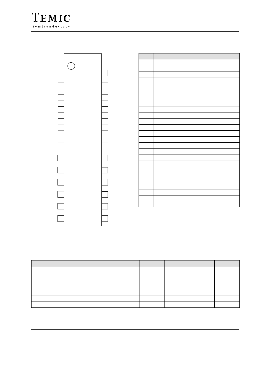
Pin Description
1
2
3
4
5
6
7
8
10
9
27
22
21
20
18
19
17
12
11
28
25
26
23
24
V
i,IF1
C
AGC,IF
GND
V
i,IF2
V
i,IF2
R
top
C
AGC,SIF
V
i,IF1
I
tun
C
Ref
V
i,SIF
V
i,SIF
V
vco
V
vco
GND
V
LO
LF
V
tun
V
AFC
V
S
V
freq
V
o,AM
V
o,FM
AGC
Ref
16
15
14
13
14530
V
out
C
bl
V
mod
V
sw
Figure 2. Pinning
Pin
Symbol
Function
¡¡¡
¡¡¡
1, 2
¡¡¡¡
¡¡¡¡
V
i,SIF
¡¡¡¡¡¡¡¡¡¡¡
¡¡¡¡¡¡¡¡¡¡¡
SIF input (symmetrical)
¡¡¡
¡¡¡
3
¡¡¡¡
¡¡¡¡
C
Ref
¡¡¡¡¡¡¡¡¡¡¡
¡¡¡¡¡¡¡¡¡¡¡
Internal reference voltage (BG)
¡¡¡
¡¡¡
4
¡¡¡¡
¡¡¡¡
C
AGC,SIF
¡¡¡¡¡¡¡¡¡¡¡
¡¡¡¡¡¡¡¡¡¡¡
SIF-AGC (time constant)
¡¡¡
¡¡¡
5, 6
¡¡¡¡
¡¡¡¡
V
i,IF1
¡¡¡¡¡¡¡¡¡¡¡
¡¡¡¡¡¡¡¡¡¡¡
IF1 input (symmetrical)
¡¡¡
¡¡¡
7
¡¡¡¡
¡¡¡¡
C
AGC,IF
¡¡¡¡¡¡¡¡¡¡¡
¡¡¡¡¡¡¡¡¡¡¡
IF-AGC (time constant)
¡¡¡
8
¡¡¡¡
GND
¡¡¡¡¡¡¡¡¡¡¡
Ground
¡¡¡
¡¡¡
9, 10
¡¡¡¡
¡¡¡¡
V
i,IF2
¡¡¡¡¡¡¡¡¡¡¡
¡¡¡¡¡¡¡¡¡¡¡
IF2 input (symmetrical)
¡¡¡
¡¡¡
11
¡¡¡¡
¡¡¡¡
R
top
¡¡¡¡¡¡¡¡¡¡¡
¡¡¡¡¡¡¡¡¡¡¡
Take over point, tuner AGC
¡¡¡
¡¡¡
12
¡¡¡¡
¡¡¡¡
I
tun
¡¡¡¡¡¡¡¡¡¡¡
¡¡¡¡¡¡¡¡¡¡¡
Tuner AGC output current
¡¡¡
¡¡¡
13
¡¡¡¡
¡¡¡¡
V
out
¡¡¡¡¡¡¡¡¡¡¡
¡¡¡¡¡¡¡¡¡¡¡
CVBS or 2nd IF output
¡¡¡
¡¡¡
14
¡¡¡¡
¡¡¡¡
C
bl
¡¡¡¡¡¡¡¡¡¡¡
¡¡¡¡¡¡¡¡¡¡¡
Capacitor ≠ black level detector
¡¡¡
¡¡¡
15
¡¡¡¡
¡¡¡¡
V
sw
¡¡¡¡¡¡¡¡¡¡¡
¡¡¡¡¡¡¡¡¡¡¡
IF input selector switch
¡¡¡
¡¡¡
16
¡¡¡¡
¡¡¡¡
V
mod
¡¡¡¡¡¡¡¡¡¡¡
¡¡¡¡¡¡¡¡¡¡¡
Modulation switch
¡¡¡
17
¡¡¡¡
V
freq
¡¡¡¡¡¡¡¡¡¡¡
VCO frequency switch
¡¡¡
¡¡¡
18
¡¡¡¡
¡¡¡¡
V
tun
¡¡¡¡¡¡¡¡¡¡¡
¡¡¡¡¡¡¡¡¡¡¡
External VCO tuning voltage
¡¡¡
¡¡¡
19
¡¡¡¡
¡¡¡¡
LF
¡¡¡¡¡¡¡¡¡¡¡
¡¡¡¡¡¡¡¡¡¡¡
Loop filter
¡¡¡
¡¡¡
20
¡¡¡¡
¡¡¡¡
V
LO
¡¡¡¡¡¡¡¡¡¡¡
¡¡¡¡¡¡¡¡¡¡¡
Local oscillator output voltage
¡¡¡
¡¡¡
21
¡¡¡¡
¡¡¡¡
GND
¡¡¡¡¡¡¡¡¡¡¡
¡¡¡¡¡¡¡¡¡¡¡
Ground
¡¡¡
¡¡¡
22, 23
¡¡¡¡
¡¡¡¡
V
vco
¡¡¡¡¡¡¡¡¡¡¡
¡¡¡¡¡¡¡¡¡¡¡
VCO circuit (symmetrical)
¡¡¡
¡¡¡
24
¡¡¡¡
¡¡¡¡
V
s
¡¡¡¡¡¡¡¡¡¡¡
¡¡¡¡¡¡¡¡¡¡¡
Supply voltage
¡¡¡
¡¡¡
25
¡¡¡¡
¡¡¡¡
V
AFC
¡¡¡¡¡¡¡¡¡¡¡
¡¡¡¡¡¡¡¡¡¡¡
AFC output
¡¡¡
26
¡¡¡¡
V
o,AM
¡¡¡¡¡¡¡¡¡¡¡
AF output ≠ AM sound
¡¡¡
¡¡¡
27
¡¡¡¡
¡¡¡¡
V
o,FM
¡¡¡¡¡¡¡¡¡¡¡
¡¡¡¡¡¡¡¡¡¡¡
Intercarrier output
¡¡¡
¡
¡
¡
¡¡¡
28
¡¡¡¡
¡
¡¡
¡
¡¡¡¡
AGC
Ref
¡¡¡¡¡¡¡¡¡¡¡
¡
¡¡¡¡¡¡¡¡¡
¡
¡¡¡¡¡¡¡¡¡¡¡
AGC reference for DVB
operation
Absolute Maximum Ratings
Parameters
Symbol
Value
Unit
¡¡¡¡¡¡¡¡¡¡¡¡¡¡¡¡¡
Supply voltage
¡¡¡¡¡
V
S
¡¡¡¡¡¡¡¡
5.5
¡¡¡¡¡
V
¡¡¡¡¡¡¡¡¡¡¡¡¡¡¡¡¡
¡¡¡¡¡¡¡¡¡¡¡¡¡¡¡¡¡
Supply current
¡¡¡¡¡
¡¡¡¡¡
I
S
¡¡¡¡¡¡¡¡
¡¡¡¡¡¡¡¡
100
¡¡¡¡¡
¡¡¡¡¡
mA
¡¡¡¡¡¡¡¡¡¡¡¡¡¡¡¡¡
¡¡¡¡¡¡¡¡¡¡¡¡¡¡¡¡¡
Power dissipation, V
S
= 5.5 V
¡¡¡¡¡
¡¡¡¡¡
P
tot
¡¡¡¡¡¡¡¡
¡¡¡¡¡¡¡¡
550
¡¡¡¡¡
¡¡¡¡¡
mW
¡¡¡¡¡¡¡¡¡¡¡¡¡¡¡¡¡
¡¡¡¡¡¡¡¡¡¡¡¡¡¡¡¡¡
Output currents
¡¡¡¡¡
¡¡¡¡¡
I
out
¡¡¡¡¡¡¡¡
¡¡¡¡¡¡¡¡
5
¡¡¡¡¡
¡¡¡¡¡
mA
¡¡¡¡¡¡¡¡¡¡¡¡¡¡¡¡¡
¡¡¡¡¡¡¡¡¡¡¡¡¡¡¡¡¡
Junction temperature
¡¡¡¡¡
¡¡¡¡¡
T
j
¡¡¡¡¡¡¡¡
¡¡¡¡¡¡¡¡
125
¡¡¡¡¡
¡¡¡¡¡
∞
C
¡¡¡¡¡¡¡¡¡¡¡¡¡¡¡¡¡
¡¡¡¡¡¡¡¡¡¡¡¡¡¡¡¡¡
Storage temperature
¡¡¡¡¡
¡¡¡¡¡
T
stg
¡¡¡¡¡¡¡¡
¡¡¡¡¡¡¡¡
≠25 to +125
¡¡¡¡¡
¡¡¡¡¡
∞
C
¡¡¡¡¡¡¡¡¡¡¡¡¡¡¡¡¡
¡¡¡¡¡¡¡¡¡¡¡¡¡¡¡¡¡
Electrostatic handling *)
¡¡¡¡¡
¡¡¡¡¡
V
ESD
¡¡¡¡¡¡¡¡
¡¡¡¡¡¡¡¡
tbd
¡¡¡¡¡
¡¡¡¡¡
V
*) Equivalent to discharging a 200-pF capacitor through a 0-
W resistor
U4479B
TELEFUNKEN Semiconductors
Rev. A2, 14-Jan-98
Preliminary Information
4 (11)
Operating Range
Parameters
Symbol
Value
Unit
¡¡¡¡¡¡¡¡¡¡¡¡¡¡¡¡¡
¡¡¡¡¡¡¡¡¡¡¡¡¡¡¡¡¡
Supply voltage range
¡¡¡¡¡
¡¡¡¡¡
V
S
¡¡¡¡¡¡¡¡
¡¡¡¡¡¡¡¡
4.5 to 5.5
¡¡¡¡¡
¡¡¡¡¡
V
¡¡¡¡¡¡¡¡¡¡¡¡¡¡¡¡¡
¡¡¡¡¡¡¡¡¡¡¡¡¡¡¡¡¡
Ambient temperature
¡¡¡¡¡
¡¡¡¡¡
T
amb
¡¡¡¡¡¡¡¡
¡¡¡¡¡¡¡¡
0 to +85
¡¡¡¡¡
¡¡¡¡¡
∞
C
Thermal Resistance
Parameters
Symbol
Value
Unit
¡¡¡¡¡¡¡¡¡¡¡¡¡¡¡¡¡
¡¡¡¡¡¡¡¡¡¡¡¡¡¡¡¡¡
Junction ambient
(when soldered to PCB)
¡¡¡¡¡
¡¡¡¡¡
R
thJA
¡¡¡¡¡¡¡¡
¡¡¡¡¡¡¡¡
75
¡¡¡¡¡
¡¡¡¡¡
K/W
Electrical Characteristics
V
S
= 5 V, T
amb
= +25
∞
C
Parameters
Test Conditions / Pins
Symbol
Min.
Typ.
Max.
Unit
¡¡¡¡¡¡¡¡¡¡¡¡¡¡¡¡¡¡¡¡¡¡¡¡¡¡¡¡¡¡¡¡
¡¡¡¡¡¡¡¡¡¡¡¡¡¡¡¡¡¡¡¡¡¡¡¡¡¡¡¡¡¡¡¡
DC supply
¡¡¡¡¡¡¡¡¡
¡¡¡¡¡¡¡¡¡
Supply voltage
¡¡¡¡¡¡¡¡¡
¡¡¡¡¡¡¡¡¡
¡¡¡¡
¡¡¡¡
V
S
¡¡¡¡
¡¡¡¡
4.5
¡¡¡¡
¡¡¡¡
5.0
¡¡¡¡
¡¡¡¡
5.5
¡¡¡¡
¡¡¡¡
V
¡¡¡¡¡¡¡¡¡
Supply current
¡¡¡¡¡¡¡¡¡
¡¡¡¡
I
S
¡¡¡¡
¡¡¡¡
80
¡¡¡¡
100
¡¡¡¡
mA
¡¡¡¡¡¡¡¡¡¡¡¡¡¡¡¡¡¡¡¡¡¡¡¡¡¡¡¡¡¡¡¡
¡¡¡¡¡¡¡¡¡¡¡¡¡¡¡¡¡¡¡¡¡¡¡¡¡¡¡¡¡¡¡¡
Video IF- and DVB IF inputs
¡¡¡¡¡¡¡¡¡
¡
¡¡¡¡¡¡¡
¡
¡¡¡¡¡¡¡¡¡
Input sensitivity,
RMS value
¡¡¡¡¡¡¡¡¡
¡
¡¡¡¡¡¡¡
¡
¡¡¡¡¡¡¡¡¡
¡¡¡¡
¡
¡¡
¡
¡¡¡¡
v
in
¡¡¡¡
¡
¡¡
¡
¡¡¡¡
¡¡¡¡
¡
¡¡
¡
¡¡¡¡
80
¡¡¡¡
¡
¡¡
¡
¡¡¡¡
120
¡¡¡¡
¡
¡¡
¡
¡¡¡¡
mV
¡¡¡¡¡¡¡¡¡
¡¡¡¡¡¡¡¡¡
Input impedance
¡¡¡¡¡¡¡¡¡
¡¡¡¡¡¡¡¡¡
See note 1
¡¡¡¡
¡¡¡¡
R
in
¡¡¡¡
¡¡¡¡
¡¡¡¡
¡¡¡¡
1.2
¡¡¡¡
¡¡¡¡
¡¡¡¡
¡¡¡¡
k
W
¡¡¡¡¡¡¡¡¡
¡¡¡¡¡¡¡¡¡
Input capacitance
¡¡¡¡¡¡¡¡¡
¡¡¡¡¡¡¡¡¡
See note 1
¡¡¡¡
¡¡¡¡
C
in
¡¡¡¡
¡¡¡¡
¡¡¡¡
¡¡¡¡
2
¡¡¡¡
¡¡¡¡
¡¡¡¡
¡¡¡¡
pF
¡¡¡¡¡¡¡¡¡¡¡¡¡¡¡¡¡¡¡¡¡¡¡¡¡¡¡¡¡¡¡¡
Video IF AGC (negative/ positive modulation)
¡¡¡¡¡¡¡¡¡
¡¡¡¡¡¡¡¡¡
IF gain control range
¡¡¡¡¡¡¡¡¡
¡¡¡¡¡¡¡¡¡
¡¡¡¡
¡¡¡¡
G
v
¡¡¡¡
¡¡¡¡
60
¡¡¡¡
¡¡¡¡
65
¡¡¡¡
¡¡¡¡
¡¡¡¡
¡¡¡¡
dB
¡¡¡¡¡¡¡¡¡
¡¡¡¡¡¡¡¡¡
AGC capacitor
¡¡¡¡¡¡¡¡¡
¡¡¡¡¡¡¡¡¡
¡¡¡¡
¡¡¡¡
C
AGC
¡¡¡¡
¡¡¡¡
¡¡¡¡
¡¡¡¡
2.2
¡¡¡¡
¡¡¡¡
¡¡¡¡
¡¡¡¡
mF
¡¡¡¡¡¡¡¡¡
¡¡¡¡¡¡¡¡¡
Black level capacitor
¡¡¡¡¡¡¡¡¡
¡¡¡¡¡¡¡¡¡
¡¡¡¡
¡¡¡¡
C
BL
¡¡¡¡
¡¡¡¡
¡¡¡¡
¡¡¡¡
100
¡¡¡¡
¡¡¡¡
¡¡¡¡
¡¡¡¡
nF
¡¡¡¡¡¡¡¡¡¡¡¡¡¡¡¡¡¡¡¡¡¡¡¡¡¡¡¡¡¡¡¡
¡¡¡¡¡¡¡¡¡¡¡¡¡¡¡¡¡¡¡¡¡¡¡¡¡¡¡¡¡¡¡¡
DVB AGC (QAM modulation)
¡¡¡¡¡¡¡¡¡
¡
¡¡¡¡¡¡¡
¡
¡¡¡¡¡¡¡¡¡
IF gain control range
¡¡¡¡¡¡¡¡¡
¡
¡¡¡¡¡¡¡
¡
¡¡¡¡¡¡¡¡¡
IF2 output voltage
Pin 13 = 1.8 Vpp
¡¡¡¡
¡
¡¡
¡
¡¡¡¡
G
v
¡¡¡¡
¡
¡¡
¡
¡¡¡¡
60
¡¡¡¡
¡
¡¡
¡
¡¡¡¡
65
¡¡¡¡
¡
¡¡
¡
¡¡¡¡
¡¡¡¡
¡
¡¡
¡
¡¡¡¡
dB
¡¡¡¡¡¡¡¡¡¡¡¡¡¡¡¡¡¡¡¡¡¡¡¡¡¡¡¡¡¡¡¡
Tuner AGC
¡¡¡¡¡¡¡¡¡
¡
¡¡¡¡¡¡¡
¡
¡¡¡¡¡¡¡¡¡
Available tuner
AGC current
¡¡¡¡¡¡¡¡¡
¡
¡¡¡¡¡¡¡
¡
¡¡¡¡¡¡¡¡¡
¡¡¡¡
¡
¡¡
¡
¡¡¡¡
I
tun
¡¡¡¡
¡
¡¡
¡
¡¡¡¡
1
¡¡¡¡
¡
¡¡
¡
¡¡¡¡
2
¡¡¡¡
¡
¡¡
¡
¡¡¡¡
4
¡¡¡¡
¡
¡¡
¡
¡¡¡¡
mA
¡¡¡¡¡¡¡¡¡
¡¡¡¡¡¡¡¡¡
Allowable output voltage
¡¡¡¡¡¡¡¡¡
¡¡¡¡¡¡¡¡¡
¡¡¡¡
¡¡¡¡
V
out
¡¡¡¡
¡¡¡¡
0.3
¡¡¡¡
¡¡¡¡
¡¡¡¡
¡¡¡¡
13.5
¡¡¡¡
¡¡¡¡
V
¡¡¡¡¡¡¡¡¡
¡¡¡¡¡¡¡¡¡
IF slip ≠ tuner AGC
¡¡¡¡¡¡¡¡¡
¡¡¡¡¡¡¡¡¡
Current I
tun
: 10% to 90%
¡¡¡¡
¡¡¡¡
G
IF
¡¡¡¡
¡¡¡¡
¡¡¡¡
¡¡¡¡
8
¡¡¡¡
¡¡¡¡
10
¡¡¡¡
¡¡¡¡
dB
¡¡¡¡¡¡¡¡¡
¡
¡¡¡¡¡¡¡
¡
¡¡¡¡¡¡¡¡¡
IF input signal for
minimum take over point
¡¡¡¡¡¡¡¡¡
¡
¡¡¡¡¡¡¡
¡
¡¡¡¡¡¡¡¡¡
¡¡¡¡
¡
¡¡
¡
¡¡¡¡
v
in
¡¡¡¡
¡
¡¡
¡
¡¡¡¡
¡¡¡¡
¡
¡¡
¡
¡¡¡¡
¡¡¡¡
¡
¡¡
¡
¡¡¡¡
4
¡¡¡¡
¡
¡¡
¡
¡¡¡¡
mV
¡¡¡¡¡¡¡¡¡
¡¡¡¡¡¡¡¡¡
IF input signal for
maximum take over point
¡¡¡¡¡¡¡¡¡
¡¡¡¡¡¡¡¡¡
¡¡¡¡
¡¡¡¡
v
in
¡¡¡¡
¡¡¡¡
40
¡¡¡¡
¡¡¡¡
¡¡¡¡
¡¡¡¡
¡¡¡¡
¡¡¡¡
mV
¡¡¡¡¡¡¡¡¡
¡
¡¡¡¡¡¡¡
¡
¡¡¡¡¡¡¡¡¡
Variation of the take over
point by temperature
¡¡¡¡¡¡¡¡¡
¡
¡¡¡¡¡¡¡
¡
¡¡¡¡¡¡¡¡¡
DT
amb
= 55
∞
C
IF AGC: G
v
= 46 dB
¡¡¡¡
¡
¡¡
¡
¡¡¡¡
Dv
in
¡¡¡¡
¡
¡¡
¡
¡¡¡¡
¡¡¡¡
¡
¡¡
¡
¡¡¡¡
2
¡¡¡¡
¡
¡¡
¡
¡¡¡¡
3
¡¡¡¡
¡
¡¡
¡
¡¡¡¡
dB

U4479B
Preliminary Information
TELEFUNKEN Semiconductors
Rev. A2, 14-Jan-98
5 (11)
Electrical Characteristics (continued)
V
S
= 5 V, T
amb
= +25
∞
C
Parameters
Test Conditions / Pins
Symbol
Min.
Typ.
Max.
Unit
¡¡¡¡¡¡¡¡¡¡¡¡¡¡¡¡¡¡¡¡¡¡¡¡¡¡¡¡¡¡¡¡
¡¡¡¡¡¡¡¡¡¡¡¡¡¡¡¡¡¡¡¡¡¡¡¡¡¡¡¡¡¡¡¡
FPLL and VCO
¡¡¡¡¡¡¡¡¡
¡¡¡¡¡¡¡¡¡
Max. oscillator frequency
¡¡¡¡¡¡¡¡¡
¡¡¡¡¡¡¡¡¡
For carrier generation
¡¡¡¡
¡¡¡¡
f
vco
¡¡¡¡
¡¡¡¡
70
¡¡¡¡
¡¡¡¡
¡¡¡¡
¡¡¡¡
¡¡¡¡
¡¡¡¡
MHz
¡¡¡¡¡¡¡¡¡
¡¡¡¡¡¡¡¡¡
Capture range
¡¡¡¡¡¡¡¡¡
¡¡¡¡¡¡¡¡¡
f
vco
= 38.9 MHz
C
vco
= 8.2 pF
¡¡¡¡
¡¡¡¡
Df
cap
¡¡¡¡
¡¡¡¡
±
1.4
¡¡¡¡
¡¡¡¡
¡¡¡¡
¡¡¡¡
¡¡¡¡
¡¡¡¡
MHz
¡¡¡¡¡¡¡¡¡
¡
¡¡¡¡¡¡¡
¡
¡
¡¡¡¡¡¡¡
¡
¡
¡¡¡¡¡¡¡
¡
¡¡¡¡¡¡¡¡¡
Oscillator drift
(free runing) as function of
temperature
¡¡¡¡¡¡¡¡¡
¡
¡¡¡¡¡¡¡
¡
¡
¡¡¡¡¡¡¡
¡
¡
¡¡¡¡¡¡¡
¡
¡¡¡¡¡¡¡¡¡
See note 2,
DT
amb
= 55
∞
C,
C
vco
= 8.2 pF,
f
vco
= 38.9 MHz
¡¡¡¡
¡
¡¡
¡
¡
¡¡
¡
¡
¡¡
¡
¡¡¡¡
Df/
DT
¡¡¡¡
¡
¡¡
¡
¡
¡¡
¡
¡
¡¡
¡
¡¡¡¡
¡¡¡¡
¡
¡¡
¡
¡
¡¡
¡
¡
¡¡
¡
¡¡¡¡
¡¡¡¡
¡
¡¡
¡
¡
¡¡
¡
¡
¡¡
¡
¡¡¡¡
≠0.3
¡¡¡¡
¡
¡¡
¡
¡
¡¡
¡
¡
¡¡
¡
¡¡¡¡
%
¡¡¡¡¡¡¡¡¡
¡¡¡¡¡¡¡¡¡
Local oscillator output
signal
¡¡¡¡¡¡¡¡¡
¡¡¡¡¡¡¡¡¡
Internal control loop
switched off
¡¡¡¡
¡¡¡¡
LO
out
¡¡¡¡
¡¡¡¡
¡¡¡¡
¡¡¡¡
100
¡¡¡¡
¡¡¡¡
¡¡¡¡
¡¡¡¡
mV
¡¡¡¡¡¡¡¡¡
¡
¡¡¡¡¡¡¡
¡
¡¡¡¡¡¡¡¡¡
Local oscillator control
signal
¡¡¡¡¡¡¡¡¡
¡
¡¡¡¡¡¡¡
¡
¡¡¡¡¡¡¡¡¡
Internal control loop
switched off
¡¡¡¡
¡
¡¡
¡
¡¡¡¡
v
tun
¡¡¡¡
¡
¡¡
¡
¡¡¡¡
0.5
¡¡¡¡
¡
¡¡
¡
¡¡¡¡
¡¡¡¡
¡
¡¡
¡
¡¡¡¡
4.5
¡¡¡¡
¡
¡¡
¡
¡¡¡¡
V
¡¡¡¡¡¡¡¡¡¡¡¡¡¡¡¡¡¡¡¡¡¡¡¡¡¡¡¡¡¡¡¡
¡¡¡¡¡¡¡¡¡¡¡¡¡¡¡¡¡¡¡¡¡¡¡¡¡¡¡¡¡¡¡¡
CVBS and 2nd IF output
¡¡¡¡¡¡¡¡¡
¡¡¡¡¡¡¡¡¡
Output current ≠source
≠sink
¡¡¡¡¡¡¡¡¡
¡¡¡¡¡¡¡¡¡
¡¡¡¡
¡¡¡¡
±
I
out
¡¡¡¡
¡¡¡¡
2
¡¡¡¡
¡¡¡¡
¡¡¡¡
¡¡¡¡
5
4
¡¡¡¡
¡¡¡¡
mA
mA
¡¡¡¡¡¡¡¡¡
¡¡¡¡¡¡¡¡¡
Output resistance
¡¡¡¡¡¡¡¡¡
¡¡¡¡¡¡¡¡¡
See note 1
¡¡¡¡
¡¡¡¡
R
out
¡¡¡¡
¡¡¡¡
¡¡¡¡
¡¡¡¡
¡¡¡¡
¡¡¡¡
100
¡¡¡¡
¡¡¡¡
W
¡¡¡¡¡¡¡¡¡
¡
¡¡¡¡¡¡¡
¡
¡
¡¡¡¡¡¡¡
¡
¡¡¡¡¡¡¡¡¡
Output amplitude
DVB signal
CVBS signal
¡¡¡¡¡¡¡¡¡
¡
¡¡¡¡¡¡¡
¡
¡
¡¡¡¡¡¡¡
¡
¡¡¡¡¡¡¡¡¡
Peak to peak value
¡¡¡¡
¡
¡¡
¡
¡
¡¡
¡
¡¡¡¡
v
o,vid
¡¡¡¡
¡
¡¡
¡
¡
¡¡
¡
¡¡¡¡
1.6
1.8
¡¡¡¡
¡
¡¡
¡
¡
¡¡
¡
¡¡¡¡
1.8
2.0
¡¡¡¡
¡
¡¡
¡
¡
¡¡
¡
¡¡¡¡
2.0
2.2
¡¡¡¡
¡
¡¡
¡
¡
¡¡
¡
¡¡¡¡
V
V
¡¡¡¡¡¡¡¡¡
¡¡¡¡¡¡¡¡¡
Difference of the CVBS sig-
nals
¡¡¡¡¡¡¡¡¡
¡¡¡¡¡¡¡¡¡
Between B/G and L
¡¡¡¡
¡¡¡¡
D
v
o,vid
¡¡¡¡
¡¡¡¡
¡¡¡¡
¡¡¡¡
¡¡¡¡
¡¡¡¡
10
¡¡¡¡
¡¡¡¡
%
¡¡¡¡¡¡¡¡¡
¡¡¡¡¡¡¡¡¡
DC output voltage
¡¡¡¡¡¡¡¡¡
¡¡¡¡¡¡¡¡¡
DVB mode
¡¡¡¡
¡¡¡¡
¡¡¡¡
¡¡¡¡
¡¡¡¡
¡¡¡¡
2.2
¡¡¡¡
¡¡¡¡
¡¡¡¡
¡¡¡¡
V
¡¡¡¡¡¡¡¡¡
¡¡¡¡¡¡¡¡¡
Sync level
¡¡¡¡¡¡¡¡¡
¡¡¡¡¡¡¡¡¡
B/G mode
¡¡¡¡
¡¡¡¡
V
sync
¡¡¡¡
¡¡¡¡
¡¡¡¡
¡¡¡¡
1.2
¡¡¡¡
¡¡¡¡
¡¡¡¡
¡¡¡¡
V
¡¡¡¡¡¡¡¡¡
¡
¡¡¡¡¡¡¡
¡
¡¡¡¡¡¡¡¡¡
Zero carrier level for
negative modulation
(Ultra white level)
¡¡¡¡¡¡¡¡¡
¡
¡¡¡¡¡¡¡
¡
¡¡¡¡¡¡¡¡¡
B/G mode
¡¡¡¡
¡
¡¡
¡
¡¡¡¡
V
DC
¡¡¡¡
¡
¡¡
¡
¡¡¡¡
¡¡¡¡
¡
¡¡
¡
¡¡¡¡
3.4
¡¡¡¡
¡
¡¡
¡
¡¡¡¡
¡¡¡¡
¡
¡¡
¡
¡¡¡¡
V
¡¡¡¡¡¡¡¡¡
¡
¡¡¡¡¡¡¡
¡
¡
¡¡¡¡¡¡¡
¡
¡¡¡¡¡¡¡¡¡
Zero carrier level for
positive modulation
(Ultra black level)
¡¡¡¡¡¡¡¡¡
¡
¡¡¡¡¡¡¡
¡
¡
¡¡¡¡¡¡¡
¡
¡¡¡¡¡¡¡¡¡
L mode
¡¡¡¡
¡
¡¡
¡
¡
¡¡
¡
¡¡¡¡
V
DC
¡¡¡¡
¡
¡¡
¡
¡
¡¡
¡
¡¡¡¡
¡¡¡¡
¡
¡¡
¡
¡
¡¡
¡
¡¡¡¡
1.14
¡¡¡¡
¡
¡¡
¡
¡
¡¡
¡
¡¡¡¡
¡¡¡¡
¡
¡¡
¡
¡
¡¡
¡
¡¡¡¡
V
¡¡¡¡¡¡¡¡¡
¡
¡¡¡¡¡¡¡
¡
¡¡¡¡¡¡¡¡¡
Supply voltage influence on
the ultra black- and ultra
white level
¡¡¡¡¡¡¡¡¡
¡
¡¡¡¡¡¡¡
¡
¡¡¡¡¡¡¡¡¡
¡¡¡¡
¡
¡¡
¡
¡¡¡¡
D
V/
V
¡¡¡¡
¡
¡¡
¡
¡¡¡¡
¡¡¡¡
¡
¡¡
¡
¡¡¡¡
1
¡¡¡¡
¡
¡¡
¡
¡¡¡¡
¡¡¡¡
¡
¡¡
¡
¡¡¡¡
%/V
¡¡¡¡¡¡¡¡¡
¡
¡¡¡¡¡¡¡
¡
¡¡¡¡¡¡¡¡¡
Bandwidth (≠1 dB) of
2nd IF, in DVB mode
¡¡¡¡¡¡¡¡¡
¡
¡¡¡¡¡¡¡
¡
¡¡¡¡¡¡¡¡¡
R
L
1 k
W, C
L
50 pF
¡¡¡¡
¡
¡¡
¡
¡¡¡¡
B
¡¡¡¡
¡
¡¡
¡
¡¡¡¡
10
¡¡¡¡
¡
¡¡
¡
¡¡¡¡
¡¡¡¡
¡
¡¡
¡
¡¡¡¡
¡¡¡¡
¡
¡¡
¡
¡¡¡¡
MHz
¡¡¡¡¡¡¡¡¡
¡¡¡¡¡¡¡¡¡
Frequency response over
AGC range
¡¡¡¡¡¡¡¡¡
¡¡¡¡¡¡¡¡¡
¡¡¡¡
¡¡¡¡
D
B
¡¡¡¡
¡¡¡¡
¡¡¡¡
¡¡¡¡
¡¡¡¡
¡¡¡¡
2.0
¡¡¡¡
¡¡¡¡
dB
¡¡¡¡¡¡¡¡¡
¡¡¡¡¡¡¡¡¡
Differential gain error
¡¡¡¡¡¡¡¡¡
¡¡¡¡¡¡¡¡¡
¡¡¡¡
¡¡¡¡
DG
¡¡¡¡
¡¡¡¡
¡¡¡¡
¡¡¡¡
2
¡¡¡¡
¡¡¡¡
5
¡¡¡¡
¡¡¡¡
%
¡¡¡¡¡¡¡¡¡
¡¡¡¡¡¡¡¡¡
Differential phase error
¡¡¡¡¡¡¡¡¡
¡¡¡¡¡¡¡¡¡
¡¡¡¡
¡¡¡¡
DP
¡¡¡¡
¡¡¡¡
¡¡¡¡
¡¡¡¡
2
¡¡¡¡
¡¡¡¡
5
¡¡¡¡
¡¡¡¡
deg
¡¡¡¡¡¡¡¡¡
¡¡¡¡¡¡¡¡¡
Intermodulation 1.07 MHz
¡¡¡¡¡¡¡¡¡
¡¡¡¡¡¡¡¡¡
See note 3
¡¡¡¡
¡¡¡¡
a
IM
¡¡¡¡
¡¡¡¡
52
¡¡¡¡
¡¡¡¡
60
¡¡¡¡
¡¡¡¡
¡¡¡¡
¡¡¡¡
dB
¡¡¡¡¡¡¡¡¡
¡¡¡¡¡¡¡¡¡
Video signal-to-noise ratio
¡¡¡¡¡¡¡¡¡
¡¡¡¡¡¡¡¡¡
Weighted , CCIR≠567
¡¡¡¡
¡¡¡¡
S/
N
¡¡¡¡
¡¡¡¡
56
¡¡¡¡
¡¡¡¡
60
¡¡¡¡
¡¡¡¡
¡¡¡¡
¡¡¡¡
dB
¡¡¡¡¡¡¡¡¡
¡
¡¡¡¡¡¡¡
¡
¡
¡¡¡¡¡¡¡
¡
¡¡¡¡¡¡¡¡¡
Residual vision carrier
fundamental wave
38.9 MHz and second
harmonic 77.8 MHz
¡¡¡¡¡¡¡¡¡
¡
¡¡¡¡¡¡¡
¡
¡
¡¡¡¡¡¡¡
¡
¡¡¡¡¡¡¡¡¡
¡¡¡¡
¡
¡¡
¡
¡
¡¡
¡
¡¡¡¡
v
res1
¡¡¡¡
¡
¡¡
¡
¡
¡¡
¡
¡¡¡¡
¡¡¡¡
¡
¡¡
¡
¡
¡¡
¡
¡¡¡¡
5
¡¡¡¡
¡
¡¡
¡
¡
¡¡
¡
¡¡¡¡
15
¡¡¡¡
¡
¡¡
¡
¡
¡¡
¡
¡¡¡¡
mV

U4479B
TELEFUNKEN Semiconductors
Rev. A2, 14-Jan-98
Preliminary Information
6 (11)
Electrical Characteristics (continued)
V
S
= 5 V, T
amb
= +25
∞
C
Parameters
Test Conditions / Pins
Symbol
Min.
Typ.
Max.
Unit
¡¡¡¡¡¡¡¡¡¡¡¡¡¡¡¡¡¡¡¡¡¡¡¡¡¡¡¡¡¡¡¡
¡¡¡¡¡¡¡¡¡¡¡¡¡¡¡¡¡¡¡¡¡¡¡¡¡¡¡¡¡¡¡¡
AFC output
¡¡¡¡¡¡¡¡¡
¡¡¡¡¡¡¡¡¡
Control slope
¡¡¡¡¡¡¡¡¡
¡¡¡¡¡¡¡¡¡
¡¡¡¡
¡¡¡¡
D
I/
D
f
¡¡¡¡
¡¡¡¡
¡¡¡¡
¡¡¡¡
0.7
¡¡¡¡
¡¡¡¡
¡¡¡¡
¡¡¡¡
mA/kHz
¡¡¡¡¡¡¡¡¡
¡¡¡¡¡¡¡¡¡
Frequency drift by
temperature
¡¡¡¡¡¡¡¡¡
¡¡¡¡¡¡¡¡¡
Related to the picture
carrier frequency
¡¡¡¡
¡¡¡¡
¡¡¡¡
¡¡¡¡
¡¡¡¡
¡¡¡¡
0.25
¡¡¡¡
¡¡¡¡
0.6
¡¡¡¡
¡¡¡¡
%
¡¡¡¡¡¡¡¡¡
¡
¡¡¡¡¡¡¡
¡
¡
¡¡¡¡¡¡¡
¡
¡¡¡¡¡¡¡¡¡
Output voltage
upper limit
lower limit
¡¡¡¡¡¡¡¡¡
¡
¡¡¡¡¡¡¡
¡
¡
¡¡¡¡¡¡¡
¡
¡¡¡¡¡¡¡¡¡
¡¡¡¡
¡
¡¡
¡
¡
¡¡
¡
¡¡¡¡
V
AFC
¡¡¡¡
¡
¡¡
¡
¡
¡¡
¡
¡¡¡¡
V
S
≠0.4
¡¡¡¡
¡
¡¡
¡
¡
¡¡
¡
¡¡¡¡
¡¡¡¡
¡
¡¡
¡
¡
¡¡
¡
¡¡¡¡
0.4
¡¡¡¡
¡
¡¡
¡
¡
¡¡
¡
¡¡¡¡
V
V
¡¡¡¡¡¡¡¡¡
¡¡¡¡¡¡¡¡¡
Output current
¡¡¡¡¡¡¡¡¡
¡¡¡¡¡¡¡¡¡
¡¡¡¡
¡¡¡¡
I
AFC
¡¡¡¡
¡¡¡¡
¡¡¡¡
¡¡¡¡
±
0.2
¡¡¡¡
¡¡¡¡
¡¡¡¡
¡¡¡¡
mA
¡¡¡¡¡¡¡¡¡¡¡¡¡¡¡¡¡¡¡¡¡¡¡¡¡¡¡¡¡¡¡¡
¡¡¡¡¡¡¡¡¡¡¡¡¡¡¡¡¡¡¡¡¡¡¡¡¡¡¡¡¡¡¡¡
SIF input
¡¡¡¡¡¡¡¡¡
¡¡¡¡¡¡¡¡¡
Input sensitivity,
RMS value
¡¡¡¡¡¡¡¡¡
¡¡¡¡¡¡¡¡¡
Output signal: ≠3 dB
¡¡¡¡
¡¡¡¡
v
in
¡¡¡¡
¡¡¡¡
¡¡¡¡
¡¡¡¡
80
¡¡¡¡
¡¡¡¡
120
¡¡¡¡
¡¡¡¡
V
¡¡¡¡¡¡¡¡¡
¡¡¡¡¡¡¡¡¡
Input impedance
¡¡¡¡¡¡¡¡¡
¡¡¡¡¡¡¡¡¡
See note 1
¡¡¡¡
¡¡¡¡
R
in
¡¡¡¡
¡¡¡¡
¡¡¡¡
¡¡¡¡
1.2
¡¡¡¡
¡¡¡¡
¡¡¡¡
¡¡¡¡
k
W
¡¡¡¡¡¡¡¡¡
¡¡¡¡¡¡¡¡¡
Input capacitance
¡¡¡¡¡¡¡¡¡
¡¡¡¡¡¡¡¡¡
See note 1
¡¡¡¡
¡¡¡¡
C
in
¡¡¡¡
¡¡¡¡
¡¡¡¡
¡¡¡¡
2
¡¡¡¡
¡¡¡¡
¡¡¡¡
¡¡¡¡
pF
¡¡¡¡¡¡¡¡¡¡¡¡¡¡¡¡¡¡¡¡¡¡¡¡¡¡¡¡¡¡¡¡
¡¡¡¡¡¡¡¡¡¡¡¡¡¡¡¡¡¡¡¡¡¡¡¡¡¡¡¡¡¡¡¡
SIF ≠ AGC
¡¡¡¡¡¡¡¡¡
¡¡¡¡¡¡¡¡¡
IF gain control range
¡¡¡¡¡¡¡¡¡
¡¡¡¡¡¡¡¡¡
¡¡¡¡
¡¡¡¡
G
v
¡¡¡¡
¡¡¡¡
60
¡¡¡¡
¡¡¡¡
65
¡¡¡¡
¡¡¡¡
¡¡¡¡
¡¡¡¡
dB
¡¡¡¡¡¡¡¡¡
¡¡¡¡¡¡¡¡¡
AGC capacitor
¡¡¡¡¡¡¡¡¡
¡¡¡¡¡¡¡¡¡
¡¡¡¡
¡¡¡¡
C
AGC
¡¡¡¡
¡¡¡¡
¡¡¡¡
¡¡¡¡
4.7
¡¡¡¡
¡¡¡¡
¡¡¡¡
¡¡¡¡
mF
¡¡¡¡¡¡¡¡¡¡¡¡¡¡¡¡¡¡¡¡¡¡¡¡¡¡¡¡¡¡¡¡
¡¡¡¡¡¡¡¡¡¡¡¡¡¡¡¡¡¡¡¡¡¡¡¡¡¡¡¡¡¡¡¡
Intercarrier output FM (see note 4)
¡¡¡¡¡¡¡¡¡
DC output voltage
¡¡¡¡¡¡¡¡¡
¡¡¡¡
V
DC
¡¡¡¡
¡¡¡¡
2
¡¡¡¡
¡¡¡¡
V
¡¡¡¡¡¡¡¡¡
¡¡¡¡¡¡¡¡¡
Output resistance
¡¡¡¡¡¡¡¡¡
¡¡¡¡¡¡¡¡¡
See note 1
¡¡¡¡
¡¡¡¡
R
out
¡¡¡¡
¡¡¡¡
¡¡¡¡
¡¡¡¡
150
¡¡¡¡
¡¡¡¡
¡¡¡¡
¡¡¡¡
W
¡¡¡¡¡¡¡¡¡
¡
¡¡¡¡¡¡¡
¡
¡¡¡¡¡¡¡¡¡
Sound IF output voltage,
RMS value
¡¡¡¡¡¡¡¡¡
¡
¡¡¡¡¡¡¡
¡
¡¡¡¡¡¡¡¡¡
5.5 MHz output voltage
v
in
= 10 mV
¡¡¡¡
¡
¡¡
¡
¡¡¡¡
v
out
¡¡¡¡
¡
¡¡
¡
¡¡¡¡
¡¡¡¡
¡
¡¡
¡
¡¡¡¡
200
¡¡¡¡
¡
¡¡
¡
¡¡¡¡
¡¡¡¡
¡
¡¡
¡
¡¡¡¡
mV
¡¡¡¡¡¡¡¡¡
¡
¡¡¡¡¡¡¡
¡
¡
¡¡¡¡¡¡¡
¡
¡
¡¡¡¡¡¡¡
¡
¡
¡¡¡¡¡¡¡
¡
¡
¡¡¡¡¡¡¡
¡
¡
¡¡¡¡¡¡¡
¡
¡
¡¡¡¡¡¡¡
¡
¡¡¡¡¡¡¡¡¡
Weighted signal-to-noise
ratio: (CCIR 468)
Black screen: Channel 1/2
Grid pattern: Channel 1/2
Grey screen 50%:
Channel 1/2
¡¡¡¡¡¡¡¡¡
¡
¡¡¡¡¡¡¡
¡
¡
¡¡¡¡¡¡¡
¡
¡
¡¡¡¡¡¡¡
¡
¡
¡¡¡¡¡¡¡
¡
¡
¡¡¡¡¡¡¡
¡
¡
¡¡¡¡¡¡¡
¡
¡
¡¡¡¡¡¡¡
¡
¡¡¡¡¡¡¡¡¡
Reference signal:
v
in
=10 mV; f
mod
= 1 kHz;
FM dev. =
±
27 kHz
tested with the double FM
demodulator U2860B;
B/G modulated IF signal
¡¡¡¡
¡
¡¡
¡
¡
¡¡
¡
¡
¡¡
¡
¡
¡¡
¡
¡
¡¡
¡
¡
¡¡
¡
¡
¡¡
¡
¡¡¡¡
S/N
S/N
S/N
¡¡¡¡
¡
¡¡
¡
¡
¡¡
¡
¡
¡¡
¡
¡
¡¡
¡
¡
¡¡
¡
¡
¡¡
¡
¡
¡¡
¡
¡¡¡¡
¡¡¡¡
¡
¡¡
¡
¡
¡¡
¡
¡
¡¡
¡
¡
¡¡
¡
¡
¡¡
¡
¡
¡¡
¡
¡
¡¡
¡
¡¡¡¡
60/58
54/52
60/57
¡¡¡¡
¡
¡¡
¡
¡
¡¡
¡
¡
¡¡
¡
¡
¡¡
¡
¡
¡¡
¡
¡
¡¡
¡
¡
¡¡
¡
¡¡¡¡
¡¡¡¡
¡
¡¡
¡
¡
¡¡
¡
¡
¡¡
¡
¡
¡¡
¡
¡
¡¡
¡
¡
¡¡
¡
¡
¡¡
¡
¡¡¡¡
dB
dB
dB
¡¡¡¡¡¡¡¡¡¡¡¡¡¡¡¡¡¡¡¡¡¡¡¡¡¡¡¡¡¡¡¡
¡¡¡¡¡¡¡¡¡¡¡¡¡¡¡¡¡¡¡¡¡¡¡¡¡¡¡¡¡¡¡¡
AF output AM (see note 5)
¡¡¡¡¡¡¡¡¡
¡¡¡¡¡¡¡¡¡
DC output voltage
¡¡¡¡¡¡¡¡¡
¡¡¡¡¡¡¡¡¡
¡¡¡¡
¡¡¡¡
V
DC
¡¡¡¡
¡¡¡¡
¡¡¡¡
¡¡¡¡
2.2
¡¡¡¡
¡¡¡¡
¡¡¡¡
¡¡¡¡
V
¡¡¡¡¡¡¡¡¡
¡¡¡¡¡¡¡¡¡
Output resistance
¡¡¡¡¡¡¡¡¡
¡¡¡¡¡¡¡¡¡
See note 1
¡¡¡¡
¡¡¡¡
R
out
¡¡¡¡
¡¡¡¡
¡¡¡¡
¡¡¡¡
150
¡¡¡¡
¡¡¡¡
¡¡¡¡
¡¡¡¡
W
¡¡¡¡¡¡¡¡¡
¡
¡¡¡¡¡¡¡
¡
¡¡¡¡¡¡¡¡¡
AF output voltage,
RMS value
¡¡¡¡¡¡¡¡¡
¡
¡¡¡¡¡¡¡
¡
¡¡¡¡¡¡¡¡¡
m = 54 %
¡¡¡¡
¡
¡¡
¡
¡¡¡¡
v
oAF
¡¡¡¡
¡
¡¡
¡
¡¡¡¡
¡¡¡¡
¡
¡¡
¡
¡¡¡¡
500
¡¡¡¡
¡
¡¡
¡
¡¡¡¡
¡¡¡¡
¡
¡¡
¡
¡¡¡¡
mV
¡¡¡¡¡¡¡¡¡
¡¡¡¡¡¡¡¡¡
Total harmonic distortion
¡¡¡¡¡¡¡¡¡
¡¡¡¡¡¡¡¡¡
m = 54%
f
mod
= 1kHz, 12.5kHz
¡¡¡¡
¡¡¡¡
THD
¡¡¡¡
¡¡¡¡
¡¡¡¡
¡¡¡¡
1
¡¡¡¡
¡¡¡¡
2
¡¡¡¡
¡¡¡¡
%
¡¡¡¡¡¡¡¡¡
¡
¡¡¡¡¡¡¡
¡
¡
¡¡¡¡¡¡¡
¡
¡¡¡¡¡¡¡¡¡
Signal-to-noise ratio
¡¡¡¡¡¡¡¡¡
¡
¡¡¡¡¡¡¡
¡
¡
¡¡¡¡¡¡¡
¡
¡¡¡¡¡¡¡¡¡
Reference:
m = 54%, f
mod
= 1 kHz,
22 kHz low-pass filter
¡¡¡¡
¡
¡¡
¡
¡
¡¡
¡
¡¡¡¡
S/N
¡¡¡¡
¡
¡¡
¡
¡
¡¡
¡
¡¡¡¡
¡¡¡¡
¡
¡¡
¡
¡
¡¡
¡
¡¡¡¡
65
¡¡¡¡
¡
¡¡
¡
¡
¡¡
¡
¡¡¡¡
¡¡¡¡
¡
¡¡
¡
¡
¡¡
¡
¡¡¡¡
dB
¡¡¡¡¡¡¡¡¡¡¡¡¡¡¡¡¡¡¡¡¡¡¡¡¡¡¡¡¡¡¡¡
¡¡¡¡¡¡¡¡¡¡¡¡¡¡¡¡¡¡¡¡¡¡¡¡¡¡¡¡¡¡¡¡
IF input switch (Pin 15)
¡¡¡¡¡¡¡¡¡
¡
¡¡¡¡¡¡¡
¡
¡¡¡¡¡¡¡¡¡
Control voltage for
HIGH: IF1 input active
LOW: IF2 input active
¡¡¡¡¡¡¡¡¡
¡
¡¡¡¡¡¡¡
¡
¡¡¡¡¡¡¡¡¡
See note 6
¡¡¡¡
¡
¡¡
¡
¡¡¡¡
Vsw
¡¡¡¡
¡
¡¡
¡
¡¡¡¡
2.5
¡¡¡¡
¡
¡¡
¡
¡¡¡¡
¡¡¡¡
¡
¡¡
¡
¡¡¡¡
3.5
1.5
¡¡¡¡
¡
¡¡
¡
¡¡¡¡
V
V
¡¡¡¡¡¡¡¡¡
¡¡¡¡¡¡¡¡¡
Switching current
¡¡¡¡¡¡¡¡¡
¡¡¡¡¡¡¡¡¡
Pin 15 to ground
¡¡¡¡
¡¡¡¡
Isw
¡¡¡¡
¡¡¡¡
¡¡¡¡
¡¡¡¡
30
¡¡¡¡
¡¡¡¡
¡¡¡¡
¡¡¡¡
mA

U4479B
Preliminary Information
TELEFUNKEN Semiconductors
Rev. A2, 14-Jan-98
7 (11)
Electrical Characteristics (continued)
V
S
= 5 V, T
amb
= +25
∞
C
Parameters
Test Conditions / Pins
Symbol
Min.
Typ.
Max.
Unit
¡¡¡¡¡¡¡¡¡¡¡¡¡¡¡¡¡¡¡¡¡¡¡¡¡¡¡¡¡¡¡¡
¡¡¡¡¡¡¡¡¡¡¡¡¡¡¡¡¡¡¡¡¡¡¡¡¡¡¡¡¡¡¡¡
Modulation switch (pin 16):
¡¡¡¡¡¡¡¡¡
¡
¡¡¡¡¡¡¡
¡
¡¡¡¡¡¡¡¡¡
Control voltage for
HIGH: neg. modulation
LOW: pos. modulation
¡¡¡¡¡¡¡¡¡
¡
¡¡¡¡¡¡¡
¡
¡¡¡¡¡¡¡¡¡
See note 6
¡¡¡¡
¡
¡¡
¡
¡¡¡¡
V
mod
¡¡¡¡
¡
¡¡
¡
¡¡¡¡
2.5
¡¡¡¡
¡
¡¡
¡
¡¡¡¡
¡¡¡¡
¡
¡¡
¡
¡¡¡¡
3.5
1.5
¡¡¡¡
¡
¡¡
¡
¡¡¡¡
V
V
¡¡¡¡¡¡¡¡¡
¡¡¡¡¡¡¡¡¡
Switching current
¡¡¡¡¡¡¡¡¡
¡¡¡¡¡¡¡¡¡
Pin 16 to ground
¡¡¡¡
¡¡¡¡
I
mod
¡¡¡¡
¡¡¡¡
¡¡¡¡
¡¡¡¡
30
¡¡¡¡
¡¡¡¡
¡¡¡¡
¡¡¡¡
mA
¡¡¡¡¡¡¡¡¡¡¡¡¡¡¡¡¡¡¡¡¡¡¡¡¡¡¡¡¡¡¡¡
¡¡¡¡¡¡¡¡¡¡¡¡¡¡¡¡¡¡¡¡¡¡¡¡¡¡¡¡¡¡¡¡
Frequency switch (Pin 17)
¡¡¡¡¡¡¡¡¡
¡
¡¡¡¡¡¡¡
¡
¡
¡¡¡¡¡¡¡
¡
¡¡¡¡¡¡¡¡¡
Control voltage for
HIGH: f
VCO
= 38.9 MHz
LOW: f
VCO
= 33.4/43 MHz
(depends on Pin 16)
¡¡¡¡¡¡¡¡¡
¡
¡¡¡¡¡¡¡
¡
¡
¡¡¡¡¡¡¡
¡
¡¡¡¡¡¡¡¡¡
see also note 6
¡¡¡¡
¡
¡¡
¡
¡
¡¡
¡
¡¡¡¡
V
freq
¡¡¡¡
¡
¡¡
¡
¡
¡¡
¡
¡¡¡¡
3.35
¡¡¡¡
¡
¡¡
¡
¡
¡¡
¡
¡¡¡¡
¡¡¡¡
¡
¡¡
¡
¡
¡¡
¡
¡¡¡¡
3.5
3.2
¡¡¡¡
¡
¡¡
¡
¡
¡¡
¡
¡¡¡¡
V
V
¡¡¡¡¡¡¡¡¡
¡¡¡¡¡¡¡¡¡
Switching current
¡¡¡¡¡¡¡¡¡
¡¡¡¡¡¡¡¡¡
Pin 17 to ground
¡¡¡¡
¡¡¡¡
I
freq
¡¡¡¡
¡¡¡¡
¡¡¡¡
¡¡¡¡
¡¡¡¡
¡¡¡¡
700
¡¡¡¡
¡¡¡¡
mA
Table of Switch Settings
¡¡¡¡¡¡¡¡¡¡¡
¡¡¡¡¡¡¡¡¡¡¡
Active IF input
¡¡¡¡¡¡¡¡¡¡¡¡
¡¡¡¡¡¡¡¡¡¡¡¡
IF 1 (Pins 5, 6)
¡¡¡¡¡¡¡¡¡¡¡
¡¡¡¡¡¡¡¡¡¡¡
IF 2 (Pins 9, 10)
¡¡¡¡¡¡¡¡¡¡¡
¡¡¡¡¡¡¡¡¡¡¡
IF input switch (Pin 15)
¡¡¡¡¡¡¡¡¡¡¡¡
¡¡¡¡¡¡¡¡¡¡¡¡
Pin 15 `high'
¡¡¡¡¡¡¡¡¡¡¡
¡¡¡¡¡¡¡¡¡¡¡
Pin 15 `low'
¡¡¡¡¡¡¡¡¡¡¡
¡¡¡¡¡¡¡¡¡¡¡
Standard
¡¡¡¡¡¡
¡¡¡¡¡¡
DVB
¡¡¡¡¡¡¡
¡¡¡¡¡¡¡
BG
¡¡¡¡¡¡
¡¡¡¡¡¡
L
¡¡¡¡¡¡
¡¡¡¡¡¡
L'
¡¡¡¡¡¡¡¡¡¡¡
¡
¡¡¡¡¡¡¡¡¡
¡
¡¡¡¡¡¡¡¡¡¡¡
VCO frequency
¡¡¡¡¡¡
¡
¡¡¡¡
¡
¡¡¡¡¡¡
43 MHz
¡¡¡¡¡¡¡
¡
¡¡¡¡¡
¡
¡¡¡¡¡¡¡
38.9 MHz
¡¡¡¡¡¡
¡
¡¡¡¡
¡
¡¡¡¡¡¡
38.9 MHz
¡¡¡¡¡¡
¡
¡¡¡¡
¡
¡¡¡¡¡¡
33.4 MHz
(see note 7)
¡¡¡¡¡¡¡¡¡¡¡
¡¡¡¡¡¡¡¡¡¡¡
Modulation switch (Pin 16)
¡¡¡¡¡¡
¡¡¡¡¡¡
`high'
¡¡¡¡¡¡¡
¡¡¡¡¡¡¡
`high'
¡¡¡¡¡¡
¡¡¡¡¡¡
`low'
¡¡¡¡¡¡
¡¡¡¡¡¡
`low'
¡¡¡¡¡¡¡¡¡¡¡
Frequency switch (Pin 17)
¡¡¡¡¡¡
`low'
¡¡¡¡¡¡¡
`high'
¡¡¡¡¡¡
`high'
¡¡¡¡¡¡
`low'
Notes
1.
This parameter is given as an application information and it is not tested during production.
2.
The oscillator drift is related to the picture carrier frequency, at external temperature-compensated LC circuit
3.
a(1.07) = 20 log (4.43 MHz component/ 1.07 MHz component);
a(1.07) value related to black-white signal
input signal conditions:
picture carrier
0 dB
color carrier
≠6 dB
sound carrier
≠24 dB
4.
Picture carrier PC = 38.9 MHz; sound carrier SC
1
= 33.4 MHz, SC
2
= 33.16 MHz;
PC/SC
1
= 13 dB; PC/SC
2
= 20 dB; PC unmodulated (equivalent to sync peak level)
5.
Sound carrier SC = 32.4 MHz, modulated with f
mod
= 1 kHz, m = 54%; v
in
= 10 mV
6.
Without control voltage `High Level' mode is automatically selected
7.
For L': AFC is adjustable with external potentiometer

U4479B
TELEFUNKEN Semiconductors
Rev. A2, 14-Jan-98
Preliminary Information
8 (11)
Basic Application Circuit
28
12
3
4
U4479B
56
7
8
9
10
11
12
13
14
27
26
25
24
23
22
21
20
19
18
17
16
15
C
10
8.2 pF
L
1
C
11
10 nF
C
12
22 F
R
4
51 k
R
5
2.2 k
R
3
51 k
W
C
13
10 nF
3.3 nF
C
14
R
2
150
C
9
470 nF
P
3
50 k
P
2
50 k
W
C
26
10 nF
C
27
10 nF
C
28
10 nF
Frequ.
Standard
VIFin
DVB
Ref
Inter≠
carrier
AM
AFC
+5 V
VCO
Frequency
Loop
filter
ext.
Loop
filter
Switching
C
5
P
1
10 k
C
6
4.7 F
C
7
Sound filter
VIF filter
DVB filter
V
Ref
AGC
Sound
SIF 1
IF 1
IF 2
AGC
V
ideo
T
uner AGC
take over
point
C
8
100 nF
Black
level
T
uner
AGC
CVBS
or 2 nd IF
1
U4744B *
2
3
4
8
7
6
5
R
1
50
W
10 nF
C
1
C
2
10 nF
IF
C
3
10 nF
C
4
2.2 F
+12 V
96 12279
W
W
W
W
m
2.2 F
m
m
2.2 F
m
W
m
current
current
* not for new development
Figure 3. Basic application circuit
U4479B
Preliminary Information
TELEFUNKEN Semiconductors
Rev. A2, 14-Jan-98
9 (11)
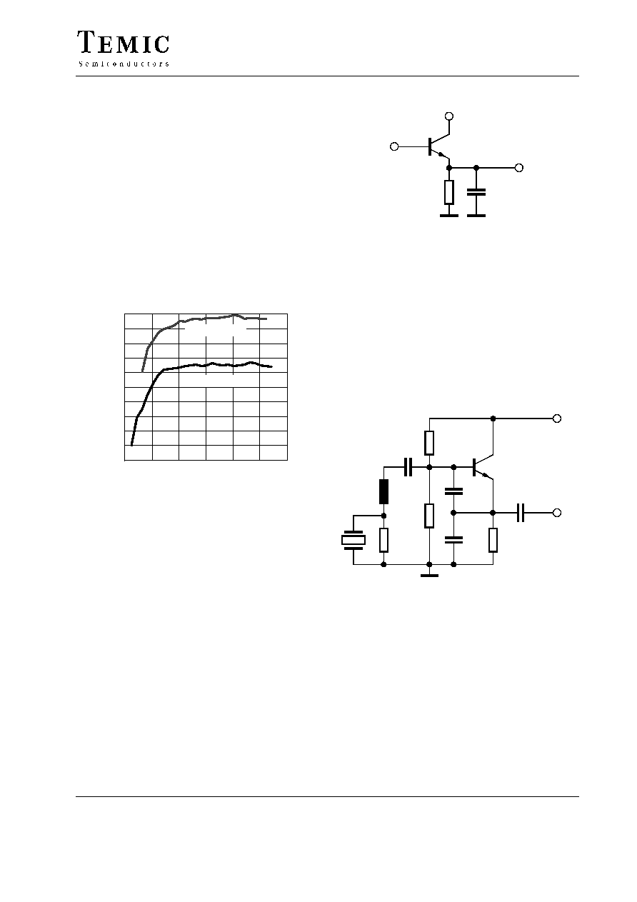
IM3 Measurements and Application Recommendations for DVB Operation
IM3 Measurement
For correct measurement of IM3 with the 2-carrier
method, it is necessary to control the internal IF amplifier
via an external voltage at Pin 7. The criteria for a correct
value of the external control voltage is the output
amplitude of 1.8 V
pp
(or lower). Please note that each
change of the input level requests a correction of the
external gain control voltage at Pin 7 in order to achieve
the 1.8-V
pp
output level again. In this case, IM3 is nearly
43 dB, independent from the input level. With an output
voltage of 1.5 V
pp
only, the IM3 is about ≠50 dB.
Anyway, if the output amplitude is more than 1.8 V
pp
(specified), the IM3 will decrease rapidly. In the graphic
below, IM3 is shown for two different conditions:
30
32
34
36
38
40
42
44
46
48
50
40
50
60
70
80
90
100
IM3 ( dB )
Input voltage (each carrier) ( dB
mV )
14778
V
out
= 1.5 V
pp
V
out
= 1.8 V
pp
Figure 4. IM3 vs. IF input voltage and IF2out voltage
Test conditions: input: f
1
= 38 MHz,
f
2
= 39 MHz, LO = 43 MHz
Circuitry for External Gain Control
If the gain control of the IC is carried out by an external
DSP, the internal charge pumps of the AGC (Pin 7) have
to be overlapped by an external voltage source. The
internal AGC currents are
±
20
µ
A. Therefore, the
minimum current capacity of the external voltage source
should be
±
30
µ
A or more.
The circuitry shown in figure 5 takes some more current.
14581
S852T
10 k
100 nF
to Pin 7
+5 V
from DSP
Figure 5.
External LO Application
If the internal VCO is not used, the LO can be fed
unbalanced or balanced to the VCO Pins 22 and 23. The
application shown below is generating an unbalanced LO
signal by using a 36-MHz third-overtone quartz
reference. The application circuit is taken from IQD
Limited Crystal Product Data Book. The LO signal is fed
unbalanced with 1 nF coupling capacity to Pin 22. Pin 23
has to be blocked to ground with an 1-nF capacitor. The
typical LO amplitude is 100 dB
µ
V. The variation of the
LO input amplitude should not exceed
±
5 dB (better:
±
3 dB).
560
100 pF
490 nH
4.7 k
47 pF
68 pF
560
1 nF
S852T
to Pin 22
+5 V
10 k
14582
Figure 6.
Note:
With external LO operation, Pin 18 (VCO tuning voltage)
should be connected to the supply voltage, and Pin 20
(LO output) should not be connected to the PCB.

U4479B
TELEFUNKEN Semiconductors
Rev. A2, 14-Jan-98
Preliminary Information
10 (11)
Package Information
13033
technical drawings
according to DIN
specifications
0.25
0.10
Package SO28
Dimensions in mm
0.4
1.27
16.51
18.05
17.80
2.35
7.5
7.3
9.15
8.65
10.50
10.20
0.25
28
15
1
14

U4479B
Preliminary Information
TELEFUNKEN Semiconductors
Rev. A2, 14-Jan-98
11 (11)
Ozone Depleting Substances Policy Statement
It is the policy of TEMIC TELEFUNKEN microelectronic GmbH to
1. Meet all present and future national and international statutory requirements.
2. Regularly and continuously improve the performance of our products, processes, distribution and operating systems
with respect to their impact on the health and safety of our employees and the public, as well as their impact on
the environment.
It is particular concern to control or eliminate releases of those substances into the atmosphere which are known as
ozone depleting substances ( ODSs ).
The Montreal Protocol ( 1987 ) and its London Amendments ( 1990 ) intend to severely restrict the use of ODSs and
forbid their use within the next ten years. Various national and international initiatives are pressing for an earlier ban
on these substances.
TEMIC TELEFUNKEN microelectronic GmbH semiconductor division has been able to use its policy of
continuous improvements to eliminate the use of ODSs listed in the following documents.
1. Annex A, B and list of transitional substances of the Montreal Protocol and the London Amendments respectively
2 . Class I and II ozone depleting substances in the Clean Air Act Amendments of 1990 by the Environmental
Protection Agency ( EPA ) in the USA
3. Council Decision 88/540/EEC and 91/690/EEC Annex A, B and C ( transitional substances ) respectively.
TEMIC can certify that our semiconductors are not manufactured with ozone depleting substances and do not contain
such substances.
We reserve the right to make changes to improve technical design and may do so without further notice.
Parameters can vary in different applications. All operating parameters must be validated for each customer
application by the customer. Should the buyer use TEMIC products for any unintended or unauthorized
application, the buyer shall indemnify TEMIC against all claims, costs, damages, and expenses, arising out of,
directly or indirectly, any claim of personal damage, injury or death associated with such unintended or
unauthorized use.
TEMIC TELEFUNKEN microelectronic GmbH, P.O.B. 3535, D-74025 Heilbronn, Germany
Telephone: 49 ( 0 ) 7131 67 2831, Fax number: 49 ( 0 ) 7131 67 2423