
U490B
TELEFUNKEN Semiconductors
Rev. A1, 29-May-96
1 (6)
One-Shot Phase Control
Description
The monolithic integrated bipolar circuit, U490B, is a
one-shot power control circuit, designed to control the
thyristor which is mainly used in electric stapler devices.
The IC is preferred to realise a one-shot phase control,
where any phase angle and thus any intensity of the load
voltage is adjustable.
After successful triggering and the following delay time,
an ignition pulse at the output is released. A further trig-
gering is only possible after the elapse of the delay time.
Features
D Phase controlled thyristor ignition
D Triggering with time delay
D Repetition time delay
D Supply current
x
2 mA
D Mains supply via resistor
Applications
D Electric stapler devices
Package: DIP8, SO8
Trigger
control
Repetition
delay
Start
delay
Sync.
Supply
stage
3
8
4
Phase control
Control
input
Ramp
POR
Output
stage
6
5
2
C
5
R
5
C
6
R
4
R
7
C
4
C
7
D
2
Load
C
2
R
2
V
S
R
1
D
1
R
3
C
3
S
1
L
N
95 10866
220 k
W
1.5 nF
24 k
W/
2 W
1N4007
47
mF/
10 V
230 V
X
V
mains
GND
150 nF
47 k
W
[68 kW
220 k
W
47 nF
7
150 nF
33
W
220
W
47 nF/
250 V
X
22 nF
C
1
Figure 1. Block diagram with external circuit
U490B
TELEFUNKEN Semiconductors
Rev. A1, 29-May-96
2 (6)
Pin Description
1
2
3
4
5
6
7
8
NC
Trigger
Sync.
GND
V
S
Ramp
Output
Contr
Pin
Symbol
Function
1
NC
Not connected
2
Trigger
Triggering
3
Sync.
Synchronization
4
GND
Ground
5
Contr
Control input
6
Ramp
Ramp
7
Output
Output
8
V
S
Supply voltage
Supply, Pin 8
Internal voltage limiter enables a simple supply from the
mains via series resistor R
1
.The supply voltage between
Pin 8 (V
S
) and ground (Pin 4) builts up via R
1
and is
smoothed by the capacitor C
1.
Series resistor R
1
can be calculated as follows:
R
1max
[ 0.85 x
V
mains
� V
Smax
2 x I
tot
where
V
mains
+ Mains supply voltage
V
Smax
+ Maximum supply voltage
I
tot
+ I
Smax
)I
X
I
Smax
+ Maximum current consumption of the IC
I
X
+ Current consumption of the
external components
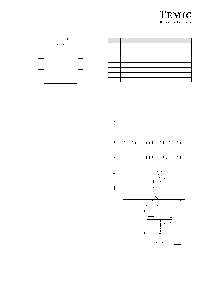
Phase Control, Pins 3, 5 and 6
The circuit is synchronized with mains supply through
Pin 3. As long as the switch S
1
is open, the circuit is in
wait state i.e., the capacitor C
6
(150 nF) is discharged and
is kept in this state (High level). When the switch S
1
is
closed, there is a current flow in Pin 2 which is evaluated
by the circuit. If this current flows after the elapse of delay
time, then the phase control is released. Capacitor, C
6
, is
then charged with I
6
+ 100 mA towards ground. At the
same time, there is a current flow of
[ 100 mA into Pin 5,
which results in voltage drop across resistor R
5
. Control
voltage, V
5
, is then 1.5 V lower internally.
The output stage is released when the ramp voltage V
6
is
equal to (V
5
* 1.5 V). When the voltage difference is
[ 150 mV, it is again turned�off.
The result is an output pulse, whose phase shift to the zero
crossing of mains voltage is determined by the resistor R
5
at control input Pin 5 (see fig. 2). Capacitor C
6
is charged
to a value of
[ 1.5 V. It remains there till the switch S
1
again opens and the repetition delay time is over.
The circuit is released, when four periods of the line volt-
age have expired after build up of the operating voltage,
before the switch S
1
is closed.
closed
open
V
8
V
8
S
1
V
3
(Sync.)
V
2
(Trigger)
V
6
(Ramp)
(Output)
0
50 ms
100 ms
150 ms
200 ms
t
V
6
V
7
t
150 mV
"X"
"X"
95 10867
t
1
V
5
� 1.5 V
V
7
t
p
Figure 2. Signal characteristics

U490B
TELEFUNKEN Semiconductors
Rev. A1, 29-May-96
3 (6)
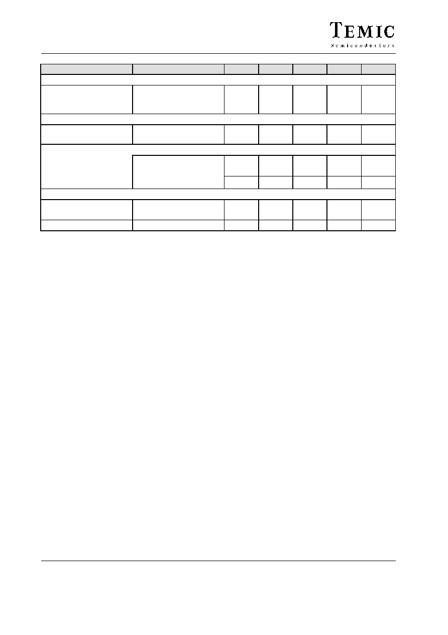
Absolute Maximum Ratings
Reference point Pin 4 (GND), unless otherwise specified
Parameters
Symbol
Value
Unit
Supply current
Pin 8
t
v
10
ms
I
S
i
s
30
150
mA
Output stage
Input voltage
Pin 7
V
I
� 0.5 V to V
S
Input current
Pin 2, 3
t
v
1 ms
"
I
I
5
30
mA
Input voltage
Pin 5, 6
V
I
0 V to V
8
Junction temperature
T
j
+125
C
Ambient temperature
T
amb
� 10 to +100
C
Storage temperature range
T
stg
� 40 to +125
C
Thermal Resistance
Parameters
Symbol
Value
Unit
Junction ambient
DIP8
SO8 on p.c.
SO8 on ceramic
R
thJA
110
220
140
K/W
Electrical Characteristics
V
S
+ 7 V, T
amb
= 25
�
C, reference point Pin 4 (GND), unless otherwise specified
Parameters
Test Conditions / Pins
Symbol
Min.
Typ.
Max.
Unit
Supply voltage limitation
I
S
+ 3 mA
Pin 8
I
S
+ 30 mA
V
S
7.2
7.4
8.2
8.4
9.2
9.4
V
Current consumption
V
S
+ 7 V
Pin 8
I
S
2
mA
Voltage monitoring
Pin 8
Switch-on threshold
Switch-off threshold
V
Son
V
Soff
5
3
V
Synchronization
Pin 3
Voltage limitation
I
3
+1 mA
Pin 3 - 8
I
3
+ �1 mA
V
lim
�V
lim
1.5
0.75
V
Switch-on threshold
Switch-off threshold
Pin 3
I
Ton
I
Toff
120
35
mA
Trigger input
Pin 2
Voltage limitation
I
2
+1 mA
Pin 2 - 8
I
2
+ �1 mA
V
lim
�V
lim
1.5
0.75
V
Switch-on threshold
Switch-off threshold
Pin 2
I
Ton
I
Toff
120
35
mA
Start delay time
Repetition delay time
f
mains
+ 50 Hz Pin 2-7
t
1
t
2
40
60
60
80
ms
U490B
TELEFUNKEN Semiconductors
Rev. A1, 29-May-96
4 (6)
Unit
Max.
Typ.
Min.
Symbol
Test Conditions / Pins
Parameters
Phase control
Pin 5, 6, 3
Control input:
Input voltage range
Input current
Pin 5
2 V
v
V
5
v
V
8
V
I
I
I
2
50
90
V
S
130
V
mA
Ramp
Pin 6
Charge current
Discharge current
2V
v
V
6
v
V
8
� 0.5 V
U
5
+ 4 V
I
ch
�I
dis
50
2
90
130
mA
mA
Phase shift
Pin 7-5
C
6
+ 150 nF
V
5
+ 2 V
t
dmax
7
ms
V
5
+ V
8
t
dmin
600
ms
Output stage, V
7
+ 0 V
Pin 7
Output reverse current
Output current
Status OFF
Status ON
"I
o(r)
�I
o
100
10
mA
mA
Pulse width
C
6
+150 nF, see figure 2
t
p
100
200
300
ms

U490B
TELEFUNKEN Semiconductors
Rev. A1, 29-May-96
5 (6)
Dimensions in mm
Package: DIP8
94 8873
Package: SO8
94 8862

U490B
TELEFUNKEN Semiconductors
Rev. A1, 29-May-96
6 (6)
Ozone Depleting Substances Policy Statement
It is the policy of TEMIC TELEFUNKEN microelectronic GmbH to
1. Meet all present and future national and international statutory requirements.
2. Regularly and continuously improve the performance of our products, processes, distribution and operating systems
with respect to their impact on the health and safety of our employees and the public, as well as their impact on
the environment.
It is particular concern to control or eliminate releases of those substances into the atmosphere which are known as
ozone depleting substances ( ODSs ).
The Montreal Protocol ( 1987 ) and its London Amendments ( 1990 ) intend to severely restrict the use of ODSs and
forbid their use within the next ten years. Various national and international initiatives are pressing for an earlier ban
on these substances.
TEMIC TELEFUNKEN microelectronic GmbH semiconductor division has been able to use its policy of
continuous improvements to eliminate the use of ODSs listed in the following documents.
1. Annex A, B and list of transitional substances of the Montreal Protocol and the London Amendments respectively
2 . Class I and II ozone depleting substances in the Clean Air Act Amendments of 1990 by the Environmental
Protection Agency ( EPA ) in the USA
3. Council Decision 88/540/EEC and 91/690/EEC Annex A, B and C ( transitional substances ) respectively.
TEMIC can certify that our semiconductors are not manufactured with ozone depleting substances and do not contain
such substances.
We reserve the right to make changes to improve technical design and may do so without further notice.
Parameters can vary in different applications. All operating parameters must be validated for each customer
application by the customer. Should the buyer use TEMIC products for any unintended or unauthorized
application, the buyer shall indemnify TEMIC against all claims, costs, damages, and expenses, arising out of,
directly or indirectly, any claim of personal damage, injury or death associated with such unintended or
unauthorized use.
TEMIC TELEFUNKEN microelectronic GmbH, P.O.B. 3535, D-74025 Heilbronn, Germany
Telephone: 49 ( 0 ) 7131 67 2831, Fax number: 49 ( 0 ) 7131 67 2423