 | –≠–ª–µ–∫—Ç—Ä–æ–Ω–Ω—ã–π –∫–æ–º–ø–æ–Ω–µ–Ω—Ç: U5020M-FP | –°–∫–∞—á–∞—Ç—å:  PDF PDF  ZIP ZIP |
U5020M
Preliminary Information
TELEFUNKEN Semiconductors
Rev. A3, 27-Feb-97
1 (8)
Digital Window Watchdog Timer
Description
The digital window watchdog timer, U5020M, is a CMOS
integrated circuit. In application where safety is critical,
it is especially important to monitor the microcontroller.
Normal microcontroller operation is indicated by a cycli-
cally transmitted trigger signal, which is received by a
window watchdog timer within a defined time window. A
missing or a wrong trigger signal makes the watchdog
timer reset the microcontroller. The IC is tailored for
microcontrollers which can work in both full-power and
sleep mode. With an additional voltage monitoring
(power-on reset and supply voltage drop reset) U5020M
offers a complete monitoring solution for microsystems
in automotive and industrial applications.
Features
D Low current consumption: I
DD
< 100
mA
D RC≠oscillator
D Internal reset during power-up and supply voltage
drops (POR)
D "Short" trigger window for active mode
"long" trigger window for sleep mode
D Cyclical wake-up of microcontroller in sleep mode
D Trigger input
D Six wake-up inputs
D Reset output
D Enable output
Ordering Information
Extended Type Number
Package
Remarks
U5020M≠FP
SO16
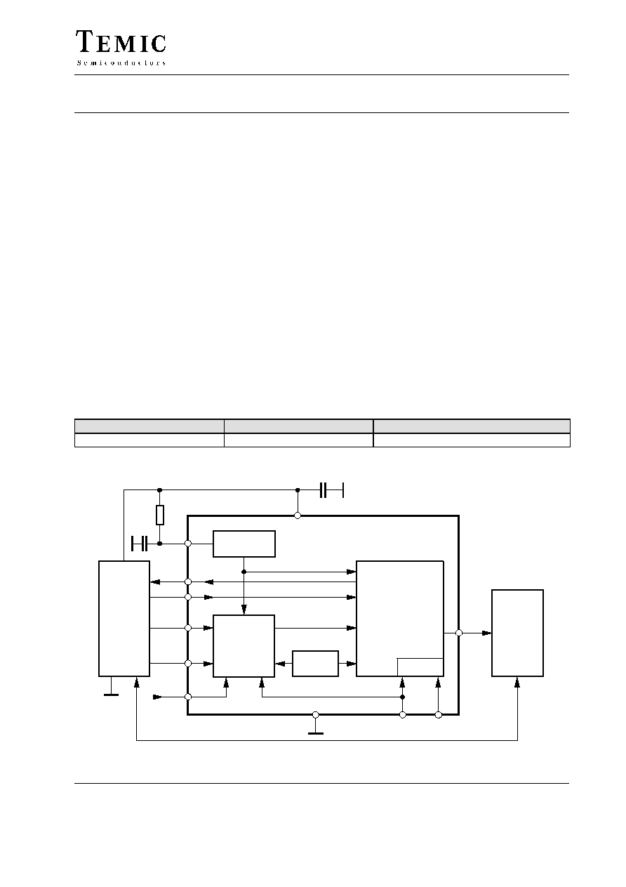
Block Diagram
Input signal
conditioning
OSC
POR
12
11
Power≠on
reset
16
10
Mode
Trigger
RC
Oscillator
State machine
POR
OSC
Reset
mC
Test logic
3≠8
2
1
Test
Test
Wake up
External
switching
circuitry
Input t
s
9
14
Enable
GND
15
13
V
DD
C
10 nF
R
1
C
1
V
DD
OSC
95 10387
Figure 1. Block diagram with external circuit
U5020M
TELEFUNKEN Semiconductors
Rev. A3, 27-Feb-97
Preliminary Information
2 (8)
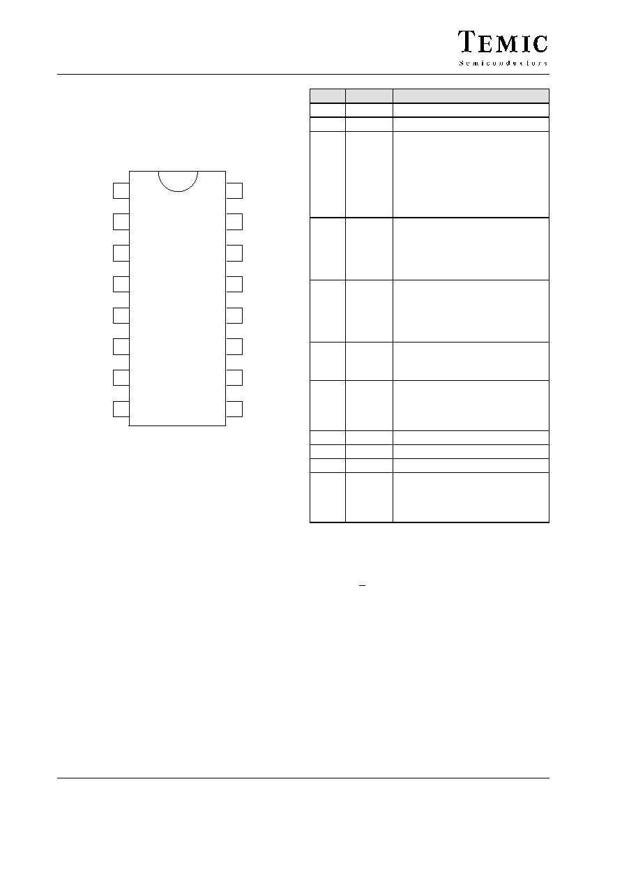
Pin
Description
1
2
3
4
5
6
7
8
16
15
14
13
12
11
10
9
Wake-up
Wake-up
95 10635
Wake-up
Wake-up
Wake-up
Wake-up
TM
TM
GND
V
DD
Mode
Trig
Reset
Ena
t
s
Osc
Figure 2. Pin connections
Pin
Symbol
Function
1
TM
Test must not be connected
2
TM
Test must be connected to GND
3 to 8
Wake-up Wake-up inputs (pull-down
resistor)
There are six digitally debounced
wake-up inputs. During the long
trigger mode each signal slope at
the inputs initiates a reset pulse at
Pin 10.
9
Ena
Enable output (push-pull)
It is used for the control of periph-
eral components. It is activated
after the processor triggers three
times correctly.
10
Reset
Reset output (open drain)
Resets the processor in the case of
a trigger error or if a wake-up
pulse occurs during the long
watchdog period.
11
Trig
Trigger input (pull-up resistor)
It is connected to the microproces-
sor's trigger signal.
12
Mode
Mode input (pull-up resistor)
The processor's mode signal initi-
ates the switchover between the
long and the short watchdog time.
13
V
DD
Supply voltage
14
GND
Ground, reference voltage
15
Osc
RC oscillator
16
t
s
Time switch input
Programming pin to select differ-
ent time durations for the long
watchdog time.
Functional
Description
Supply, Pin 13
The U5020M requires a stabilized supply voltage
V
DD
= 5 V
" 5% to comply with its electrical
characteristic.
An external buffer capacitor of C = 10 nF may be
connected between Pin 13 and GND.
RC-Oscillator, Pin 15
The clock frequency, f, can be adjusted with the
components R
1
and C
1
according to the formula:
f
+ 1
t
where t
+ 1.35 ) 1.57 R
1
(C
1
) 0.01)
R
1
in k
W, C
1
in nF and t in
ms
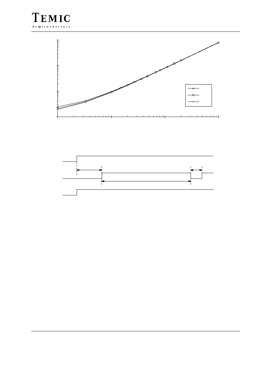
The clock frequency determines all time periods of the
logic part as shown in the last section of the data sheet
(timing). With an appropriate selection of components,
the clock frequency, f, is nearly independent of the supply
voltage as shown in figure 3. Frequency tolerance
Df
max
= 10% with R
1
" 1%, C
1
=
" 5%.
U5020M
Preliminary Information
TELEFUNKEN Semiconductors
Rev. A3, 27-Feb-97
3 (8)
1.00
10.00
100.00
1000.00
1
10
100
1000
t (
ms)
C
1
= 500 pF
4.5 V
5.5 V
5.0 V
R
1
(k
W)
95 10636
Figure 3. Period t vs. R
1
, @ C
1
= 500 pF
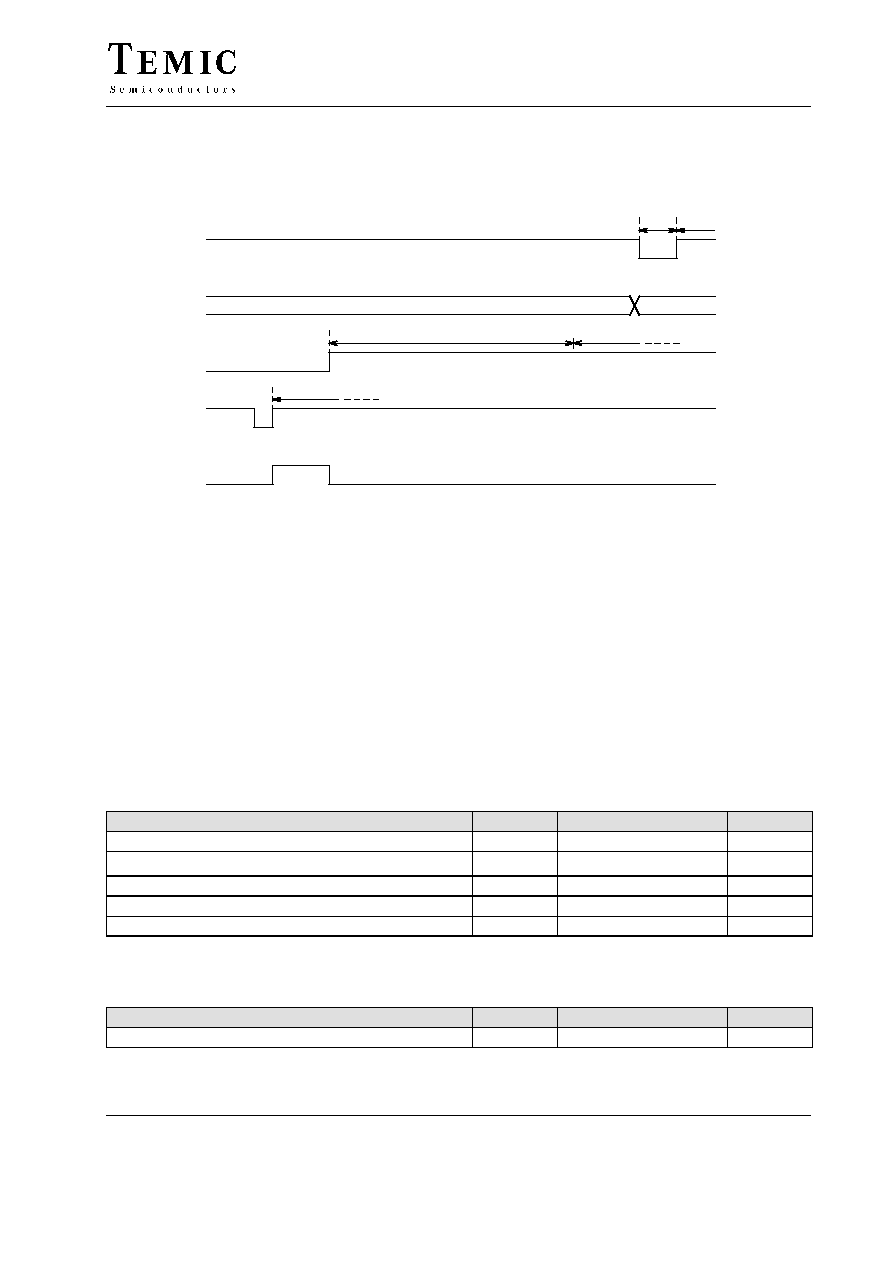
t
t
1
t
6
o
Reset Out
Mode
V
DD
Pin 13
Pin 10
Pin 12
95 10637
Figure 4. Power-up reset and mode switchover
Supply Voltage Monitoring, Pin 10
The integrated power-on reset (POR) circuitry sets the
internal logic to a defined basic status and generates a
reset pulse at the reset output, Pin 10, during ramp-up of
the supply voltage and in the case of voltage drops of the
supply. A hysteresis in the POR threshold prevents the
circuit from oscillating. During ramp≠up of the supply
voltage the reset output stays active for time, t
o
, in order
to bring the microcontroller in its defined reset status (see
figure 4). Pin 10 has an open-drain output.
Switch-over Mode Time, Pin 12
The switch-over mode time enables the synchronous
operation of micro and watchdog. After the power-up
reset time the watchdog has to be switched to its
monitoring mode by the micro with a "low" signal
transmitted to the mode pin (Pin 12) within the time out
period, t
1
,. If the low signal does not occur within time,
t
1
, (see figure 4) the watchdog generates a reset pulse, t
6
,
and the time, t
1
, starts again. Micro and watchdog are
synchronized with the switchover mode time, t
1
, each
time a reset pulse is generated.
Microcontroller in Active Mode
Monitoring with the "Short" Trigger
Window
After the switch-over mode the watchdog works in the
short watchdog mode and expects a trigger pulse from the
microcontroller within the defined time window, t
3
,
(enable time). The watchdog generates a reset pulse
which resets the microcontroller if
D the trigger pulse duration is too long,
D the trigger pulse is within the disable time, t
2
D there is no trigger pulse
Figure 5 shows the pulse diagram with a missing trigger
pulse.

U5020M
TELEFUNKEN Semiconductors
Rev. A3, 27-Feb-97
Preliminary Information
4 (8)
3
2
t
1
t
o
t
t
V
Mode
Trigger
Reset Out
DD
Pin 11
Pin 12
Pin 10
Pin 13
95 10638
Figure 5. Pulse diagram with no trigger pulse during the short watchdog time
Figure 6 shows a correct trigger sequence. The positive
edge of the trigger signal starts a new monitoring cycle
with the disable time, t
2
. To ensure a correct operation of
the microcontroller the watchdog needs to be triggered
three times correctly before it sets its enable output. This
feature is used to activate or deactivate safety critical
components, which have to be switched to a certain
condition (emergency status) in the case of a micro-
controller malfunction. As soon as there is an incorrect
trigger sequence the enable signal is reset and it takes
again a three correct trigger sequence before enable is re-
set.
Microcontroller in Sleep Mode
Monitoring with the "Long" Trigger
Window
The long watchdog mode allows cyclical wake up of the
micro during the sleep mode. Like in the short watchdog
mode there is a disable time, t
4
, and an enable time, t
5
, in
which a trigger signal is accepted. The watchdog can be
switched from the short trigger window to the long trigger
window with a "high" potential at the mode pin (Pin 12).
In contrast to the short watchdog mode the time periods
are now much longer and the enable output remains
inactive that other components can be switched off to
effect a further decrease in current consumption. As soon
as a wake-up signal at one of the 6 wake up inputs (Pins
3 to 8) is detected, the long watchdog mode ends, a reset
pulse wakes-up the sleeping microcontroller and the
normal monitoring cycle starts with the mode switch-over
time.
With the help of a low or high potential at Pin 16 (time
switch) the long watchdog time can be selected in two
values.
V
Reset Out
Mode
Trigger
Enable
t
t
t
t
t
t
trig
2
1
0
3
2
DD
Pin 9
Pin 11
Pin 12
Pin 10
Pin 13
95 10639
Figure 6. Pulse diagram of a correct trigger sequence during the short watchdog time
U5020M
Preliminary Information
TELEFUNKEN Semiconductors
Rev. A3, 27-Feb-97
5 (8)
Figure 7 shows the switch-over from the short to the long
watchdog mode. The wake up signal during the enable
time, t
5
, activates a reset pulse, t
6
.
The watchdog can be switched back from the long to the
short watchdog mode with a low potential at the mode pin
(Pin 12).
1
6
t
5
4
t
2
t
t
t
Wake-up
Enable
Mode
Trigger
Reset out
Pin
Pin 11
Pin 12
Pins 3 to 8
Pin 10
9
95 10640
Figure 7. Pulse diagram of the long watchdog time
Application Hint
In order to prevent the IC from an undesired reset output signal which may be caused by transcients on the supply under
certain conditions a pc board connection from Pin 2 to GND is strongly recommended.
Absolute Maximum Ratings
Parameters
Symbol
Value
Unit
¡¡¡¡¡¡¡¡¡¡¡¡¡¡¡¡¡
Supply voltage
¡¡¡¡¡
V
DD
¡¡¡¡¡¡¡¡
6.5
¡¡¡¡¡
V
¡¡¡¡¡¡¡¡¡¡¡¡¡¡¡¡¡
¡
¡¡¡¡¡¡¡¡¡¡¡¡¡¡¡
¡
¡¡¡¡¡¡¡¡¡¡¡¡¡¡¡¡¡
Output current
¡¡¡¡¡
¡
¡¡¡
¡
¡¡¡¡¡
I
OUT
¡¡¡¡¡¡¡¡
¡
¡¡¡¡¡¡
¡
¡¡¡¡¡¡¡¡
" 2
¡¡¡¡¡
¡
¡¡¡
¡
¡¡¡¡¡
mA
¡¡¡¡¡¡¡¡¡¡¡¡¡¡¡¡¡
¡¡¡¡¡¡¡¡¡¡¡¡¡¡¡¡¡
Input voltage
¡¡¡¡¡
¡¡¡¡¡
V
IN
¡¡¡¡¡¡¡¡
¡¡¡¡¡¡¡¡
≠0.5 V to V
DD
+ 0.5 V
¡¡¡¡¡
¡¡¡¡¡
V
¡¡¡¡¡¡¡¡¡¡¡¡¡¡¡¡¡
¡¡¡¡¡¡¡¡¡¡¡¡¡¡¡¡¡
Ambient temperature range
¡¡¡¡¡
¡¡¡¡¡
T
amb
¡¡¡¡¡¡¡¡
¡¡¡¡¡¡¡¡
≠40 to +85
¡¡¡¡¡
¡¡¡¡¡
∞
C
¡¡¡¡¡¡¡¡¡¡¡¡¡¡¡¡¡
¡¡¡¡¡¡¡¡¡¡¡¡¡¡¡¡¡
Storage temperature range
¡¡¡¡¡
¡¡¡¡¡
T
stg
¡¡¡¡¡¡¡¡
¡¡¡¡¡¡¡¡
≠55 to +150
¡¡¡¡¡
¡¡¡¡¡
∞
C
Thermal Resistance
Parameters
Symbol
Value
Unit
¡¡¡¡¡¡¡¡¡¡¡¡¡¡¡¡¡
¡¡¡¡¡¡¡¡¡¡¡¡¡¡¡¡¡
Junction ambient
SO16
¡¡¡¡¡
¡¡¡¡¡
R
thJA
¡¡¡¡¡¡¡¡
¡¡¡¡¡¡¡¡
160
¡¡¡¡¡
¡¡¡¡¡
K/W