 | –≠–ª–µ–∫—Ç—Ä–æ–Ω–Ω—ã–π –∫–æ–º–ø–æ–Ω–µ–Ω—Ç: U6206B | –°–∫–∞—á–∞—Ç—å:  PDF PDF  ZIP ZIP |
TELEFUNKEN Semiconductors
U6206B
Rev. A1: 25.10.1995
1 (8)
1.3 GHz PLL for TV- and VCR- Tuner
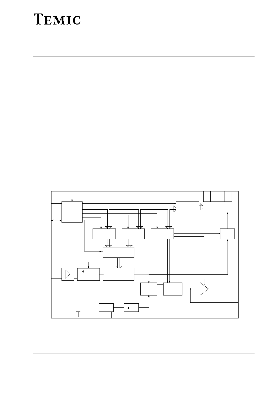
Description
The U6206B is a single chip PLL frequency synthesizer
with unidirectional I
2
C bus control. This IC contains a
high frequency prescaler which can be switched off.
5 open collector switching outputs are available.
Features
D 1.3 GHz divide-by-8 prescaler integrated
(can be bypassed)
D 15 bit counter accepts input frequencies up to
170 MHz
D mP-controlled by I
2
C-Bus
D 5 switching outputs (open collector )
D 4 addresses selectable at Pin 8 for multituner
application
D 62.5 kHz (≠1.3 GHz)/ 7.8125 kHz (≠170 MHz) tuning
steps
D Electrostatic protection according to MILSTD 883
D SO16 small package
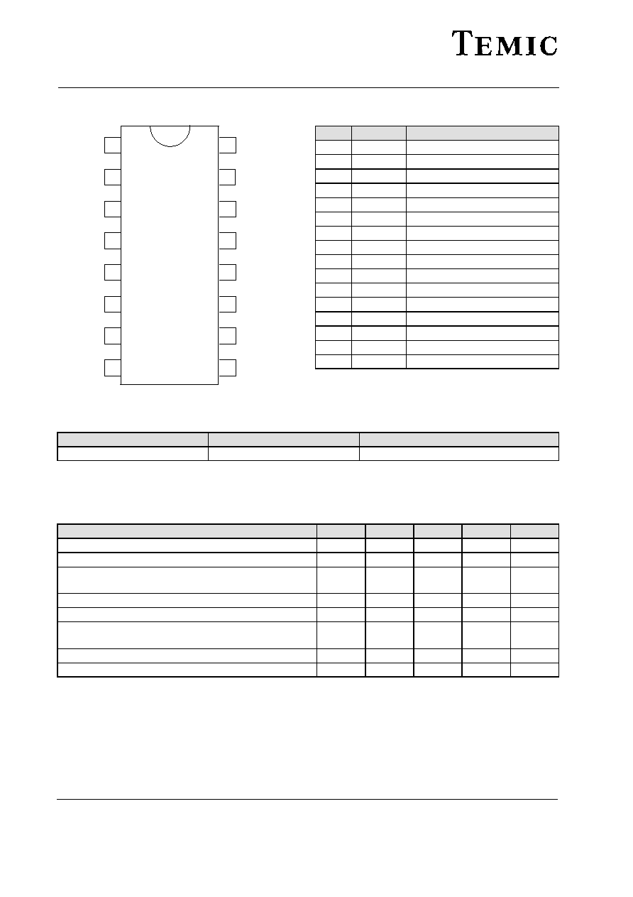
Package: SO16
Block Diagram
SW7
SW1
SW2
ADDRESS SELECTION (AS)
I C≠BUS
CONTROL
SCL
SDA
5 BIT LATCH
SWITCHING
OUTPUTS
5 BIT LATCH
8 BIT LATCH
7 BIT LATCH
15 BIT LATCH
PD
15 BIT COUNTER
1 OR 8
RFi
PHASE
COMPAR.
CHARGE
PUMP
VD
512
OSC
6
9
8
4
5
1
14
13
16
12
15
2
3
Vs
PRESCALER
GND
CRYSTAL
GATE
PSC
T1
OS
T0
5I
2
7
10
11
SW0
SW4
95 10723
Figure 1.
TELEFUNKEN Semiconductors
U6206B
Rev. A1: 25.10.1995
2 (8)
Pin Configuration
1
2
3
4
5
6
7
8
16
15
14
13
12
11
10
9
Q2
SDA
95 10722
SCL
SW7
SW4
AS
PD
Q1
RFi
RFi
V
S
SW0
SW1
SW2
VD
GND
Pin
Symbol
Function
¡¡¡
¡¡¡
1
¡¡¡¡
¡¡¡¡
PD
¡¡¡¡¡¡¡¡¡¡¡
¡¡¡¡¡¡¡¡¡¡¡
Charge pump output
¡¡¡
¡¡¡
2
¡¡¡¡
¡¡¡¡
Q1
¡¡¡¡¡¡¡¡¡¡¡
¡¡¡¡¡¡¡¡¡¡¡
Crystal
¡¡¡
¡¡¡
3
¡¡¡¡
¡¡¡¡
Q2
¡¡¡¡¡¡¡¡¡¡¡
¡¡¡¡¡¡¡¡¡¡¡
Crystal
¡¡¡
¡¡¡
4
¡¡¡¡
¡¡¡¡
SDA
¡¡¡¡¡¡¡¡¡¡¡
¡¡¡¡¡¡¡¡¡¡¡
Data in/output
¡¡¡
¡¡¡
5
¡¡¡¡
¡¡¡¡
SCL
¡¡¡¡¡¡¡¡¡¡¡
¡¡¡¡¡¡¡¡¡¡¡
Clock
¡¡¡
¡¡¡
6
¡¡¡¡
¡¡¡¡
SW7
¡¡¡¡¡¡¡¡¡¡¡
¡¡¡¡¡¡¡¡¡¡¡
Switching output open collector
¡¡¡
¡¡¡
7
¡¡¡¡
¡¡¡¡
SW4
¡¡¡¡¡¡¡¡¡¡¡
¡¡¡¡¡¡¡¡¡¡¡
Switching output open collector
¡¡¡
¡¡¡
8
¡¡¡¡
¡¡¡¡
AS
¡¡¡¡¡¡¡¡¡¡¡
¡¡¡¡¡¡¡¡¡¡¡
Address select
¡¡¡
¡¡¡
9
¡¡¡¡
¡¡¡¡
SW2
¡¡¡¡¡¡¡¡¡¡¡
¡¡¡¡¡¡¡¡¡¡¡
Switching output open collector
¡¡¡
¡¡¡
10
¡¡¡¡
¡¡¡¡
SW1
¡¡¡¡¡¡¡¡¡¡¡
¡¡¡¡¡¡¡¡¡¡¡
Switching output open collector
¡¡¡
¡¡¡
11
¡¡¡¡
¡¡¡¡
SW0
¡¡¡¡¡¡¡¡¡¡¡
¡¡¡¡¡¡¡¡¡¡¡
Switching output open collector
¡¡¡
¡¡¡
12
¡¡¡¡
¡¡¡¡
Vs
¡¡¡¡¡¡¡¡¡¡¡
¡¡¡¡¡¡¡¡¡¡¡
Supply voltage
¡¡¡
¡¡¡
13
¡¡¡¡
¡¡¡¡
RFi
¡¡¡¡¡¡¡¡¡¡¡
¡¡¡¡¡¡¡¡¡¡¡
RF input
¡¡¡
¡¡¡
14
¡¡¡¡
¡¡¡¡
RFi
¡¡¡¡¡¡¡¡¡¡¡
¡¡¡¡¡¡¡¡¡¡¡
RF input
¡¡¡
¡¡¡
15
¡¡¡¡
¡¡¡¡
GND
¡¡¡¡¡¡¡¡¡¡¡
¡¡¡¡¡¡¡¡¡¡¡
Ground
¡¡¡
¡¡¡
16
¡¡¡¡
¡¡¡¡
VD
¡¡¡¡¡¡¡¡¡¡¡
¡¡¡¡¡¡¡¡¡¡¡
Active filter output
Ordering Information
Extended Type Number
Package
Remarks
U6206B-FPG3
SO16
Taped and reeled
Absolute Maximum Ratings
All voltages are referred to GND (Pin 15).
Parameters
Symbol
Min.
Typ.
Max.
Unit
¡¡¡¡¡¡¡¡¡¡¡¡¡¡¡¡¡
¡¡¡¡¡¡¡¡¡¡¡¡¡¡¡¡¡
Supply voltage
Pin 12
¡¡¡¡
¡¡¡¡
Vs
¡¡¡¡
¡¡¡¡
≠0.3
¡¡¡¡
¡¡¡¡
¡¡¡¡
¡¡¡¡
6
¡¡¡¡
¡¡¡¡
V
¡¡¡¡¡¡¡¡¡¡¡¡¡¡¡¡¡
¡¡¡¡¡¡¡¡¡¡¡¡¡¡¡¡¡
RF input voltage
Pins 13,14
¡¡¡¡
¡¡¡¡
RFi
¡¡¡¡
¡¡¡¡
≠0.3
¡¡¡¡
¡¡¡¡
¡¡¡¡
¡¡¡¡
Vs
¡¡¡¡
¡¡¡¡
V
¡¡¡¡¡¡¡¡¡¡¡¡¡¡¡¡¡
¡
¡¡¡¡¡¡¡¡¡¡¡¡¡¡¡
¡
¡¡¡¡¡¡¡¡¡¡¡¡¡¡¡¡¡
Bus input/output voltage
Pin 4
Pin 5
¡¡¡¡
¡
¡¡
¡
¡¡¡¡
VSDA
VSCL
¡¡¡¡
¡
¡¡
¡
¡¡¡¡
≠0.3
≠0.3
¡¡¡¡
¡
¡¡
¡
¡¡¡¡
¡¡¡¡
¡
¡¡
¡
¡¡¡¡
Vs
Vs
¡¡¡¡
¡
¡¡
¡
¡¡¡¡
V
V
¡¡¡¡¡¡¡¡¡¡¡¡¡¡¡¡¡
¡¡¡¡¡¡¡¡¡¡¡¡¡¡¡¡¡
SDA output current
Open collector Pin 4
¡¡¡¡
¡¡¡¡
ISDA
¡¡¡¡
¡¡¡¡
≠1
¡¡¡¡
¡¡¡¡
¡¡¡¡
¡¡¡¡
5
¡¡¡¡
¡¡¡¡
mA
¡¡¡¡¡¡¡¡¡¡¡¡¡¡¡¡¡
Address select voltage
Pin 8
¡¡¡¡
VAS
¡¡¡¡
≠0.3
¡¡¡¡
¡¡¡¡
Vs
¡¡¡¡
V
¡¡¡¡¡¡¡¡¡¡¡¡¡¡¡¡¡
¡
¡¡¡¡¡¡¡¡¡¡¡¡¡¡¡
¡
¡¡¡¡¡¡¡¡¡¡¡¡¡¡¡¡¡
Current switching outputs Open collector Pins 11,10
Pins 9,7,6
¡¡¡¡
¡
¡¡
¡
¡¡¡¡
SW 0,1,
2,4,7
¡¡¡¡
¡
¡¡
¡
¡¡¡¡
≠1
¡¡¡¡
¡
¡¡
¡
¡¡¡¡
¡¡¡¡
¡
¡¡
¡
¡¡¡¡
15
¡¡¡¡
¡
¡¡
¡
¡¡¡¡
mA
¡¡¡¡¡¡¡¡¡¡¡¡¡¡¡¡¡
¡¡¡¡¡¡¡¡¡¡¡¡¡¡¡¡¡
Junction temperature
¡¡¡¡
¡¡¡¡
Tj
¡¡¡¡
¡¡¡¡
≠40
¡¡¡¡
¡¡¡¡
¡¡¡¡
¡¡¡¡
125
¡¡¡¡
¡¡¡¡
C
¡¡¡¡¡¡¡¡¡¡¡¡¡¡¡¡¡
¡¡¡¡¡¡¡¡¡¡¡¡¡¡¡¡¡
Storage temperature
¡¡¡¡
¡¡¡¡
Tstg
¡¡¡¡
¡¡¡¡
≠40
¡¡¡¡
¡¡¡¡
¡¡¡¡
¡¡¡¡
125
¡¡¡¡
¡¡¡¡
C
TELEFUNKEN Semiconductors
U6206B
Rev. A1: 25.10.1995
3 (8)
Operating Range
All voltages are referred to GND (Pin 15).
Parameters
Test Conditions / Pins
Symbol
Min.
Typ.
Max.
Unit
¡¡¡¡¡¡¡¡¡
¡¡¡¡¡¡¡¡¡
Supply voltage
¡¡¡¡¡¡¡¡¡
¡¡¡¡¡¡¡¡¡
Pin 12
¡¡¡¡
¡¡¡¡
Vs
¡¡¡¡
¡¡¡¡
4.5
¡¡¡¡
¡¡¡¡
¡¡¡¡
¡¡¡¡
5.5
¡¡¡¡
¡¡¡¡
V
¡¡¡¡¡¡¡¡¡
¡¡¡¡¡¡¡¡¡
Ambient temperature
¡¡¡¡¡¡¡¡¡
¡¡¡¡¡¡¡¡¡
¡¡¡¡
¡¡¡¡
T
amb
¡¡¡¡
¡¡¡¡
0
¡¡¡¡
¡¡¡¡
¡¡¡¡
¡¡¡¡
70
¡¡¡¡
¡¡¡¡
C
¡¡¡¡¡¡¡¡¡
¡¡¡¡¡¡¡¡¡
Input frequency
¡¡¡¡¡¡¡¡¡
¡¡¡¡¡¡¡¡¡
PSC = 1
Pins 13,14
¡¡¡¡
¡¡¡¡
RFi
¡¡¡¡
¡¡¡¡
64
¡¡¡¡
¡¡¡¡
¡¡¡¡
¡¡¡¡
1300
¡¡¡¡
¡¡¡¡
MHz
¡¡¡¡¡¡¡¡¡
Input frequency
¡¡¡¡¡¡¡¡¡
PSC = 0
Pins 13,14
¡¡¡¡
RFi
¡¡¡¡
1
¡¡¡¡
¡¡¡¡
170
¡¡¡¡
MHz
¡¡¡¡¡¡¡¡¡
¡¡¡¡¡¡¡¡¡
Progr. divider
¡¡¡¡¡¡¡¡¡
¡¡¡¡¡¡¡¡¡
¡¡¡¡
¡¡¡¡
SF
¡¡¡¡
¡¡¡¡
256
¡¡¡¡
¡¡¡¡
¡¡¡¡
¡¡¡¡
32767
¡¡¡¡
¡¡¡¡
Thermal Resistance
Parameters
Symbol
Value
Unit
SO16 small
RthJA
110
K/W
Electrical Characteristics
Test Conditions (unless otherwise specified) : Vs = 5V, Tamb = 25 C.
Parameters
Test Conditions / Pins
Symbol
Min.
Typ.
Max.
Unit
¡¡¡¡¡¡¡¡¡
¡
¡¡¡¡¡¡¡
¡
¡¡¡¡¡¡¡¡¡
Supply current
¡¡¡¡¡¡¡¡¡
¡
¡¡¡¡¡¡¡
¡
¡¡¡¡¡¡¡¡¡
SW 0,1,2,4,7 = 0 ; PSC =1
Pin 12
¡¡¡¡
¡
¡¡
¡
¡¡¡¡
Is
¡¡¡¡
¡
¡¡
¡
¡¡¡¡
32
¡¡¡¡
¡
¡¡
¡
¡¡¡¡
42
¡¡¡¡
¡
¡¡
¡
¡¡¡¡
52
¡¡¡¡
¡
¡¡
¡
¡¡¡¡
mA
¡¡¡¡¡¡¡¡¡
¡
¡¡¡¡¡¡¡
¡
¡¡¡¡¡¡¡¡¡
¡¡¡¡¡¡¡¡¡
¡
¡¡¡¡¡¡¡
¡
¡¡¡¡¡¡¡¡¡
SW 0,1,2,4,7 = 0 ; PSC =0
Pin 12
¡¡¡¡
¡
¡¡
¡
¡¡¡¡
Is
¡¡¡¡
¡
¡¡
¡
¡¡¡¡
22
¡¡¡¡
¡
¡¡
¡
¡¡¡¡
28
¡¡¡¡
¡
¡¡
¡
¡¡¡¡
35
¡¡¡¡
¡
¡¡
¡
¡¡¡¡
mA
¡¡¡¡¡¡¡¡¡¡¡¡¡¡¡¡¡¡¡¡¡¡¡¡¡¡¡¡¡¡¡¡
¡¡¡¡¡¡¡¡¡¡¡¡¡¡¡¡¡¡¡¡¡¡¡¡¡¡¡¡¡¡¡¡
Input sensitivity
¡¡¡¡¡¡¡¡¡
fi = 80 ≠ 1000 MHz
¡¡¡¡¡¡¡¡¡
PSC = 1
Pin 13
¡¡¡¡
Vi 1)
¡¡¡¡
¡¡¡¡
¡¡¡¡
10
¡¡¡¡
mV
¡¡¡¡¡¡¡¡¡
¡¡¡¡¡¡¡¡¡
fi = 1300 MHz
¡¡¡¡¡¡¡¡¡
¡¡¡¡¡¡¡¡¡
PSC = 1
Pin 13
¡¡¡¡
¡¡¡¡
Vi 1)
¡¡¡¡
¡¡¡¡
¡¡¡¡
¡¡¡¡
¡¡¡¡
¡¡¡¡
40
¡¡¡¡
¡¡¡¡
mV
¡¡¡¡¡¡¡¡¡
¡¡¡¡¡¡¡¡¡
fi = 10 ≠ 170 MHz
¡¡¡¡¡¡¡¡¡
¡¡¡¡¡¡¡¡¡
PSC = 0
Pin 13
¡¡¡¡
¡¡¡¡
Vi 1)
¡¡¡¡
¡¡¡¡
¡¡¡¡
¡¡¡¡
¡¡¡¡
¡¡¡¡
10
¡¡¡¡
¡¡¡¡
mV
¡¡¡¡¡¡¡¡¡
¡¡¡¡¡¡¡¡¡
Maximum input signal
¡¡¡¡¡¡¡¡¡
¡¡¡¡¡¡¡¡¡
PSC = 0 / 1
Pin 13
¡¡¡¡
¡¡¡¡
Vimax 1)
¡¡¡¡
¡¡¡¡
315
¡¡¡¡
¡¡¡¡
¡¡¡¡
¡¡¡¡
¡¡¡¡
¡¡¡¡
mV
¡¡¡¡¡¡¡¡¡¡¡¡¡¡¡¡¡¡¡¡¡¡¡¡¡¡¡¡¡¡¡¡
¡¡¡¡¡¡¡¡¡¡¡¡¡¡¡¡¡¡¡¡¡¡¡¡¡¡¡¡¡¡¡¡
Open coll. sw. outputs
Pins 11, 10, 9, 7, 6; SW 0,1,2,4,7
¡¡¡¡¡¡¡¡¡
¡¡¡¡¡¡¡¡¡
Reverse current
¡¡¡¡¡¡¡¡¡
¡¡¡¡¡¡¡¡¡
VH = 13.5 V
¡¡¡¡
¡¡¡¡
IRH
¡¡¡¡
¡¡¡¡
¡¡¡¡
¡¡¡¡
¡¡¡¡
¡¡¡¡
10
¡¡¡¡
¡¡¡¡
uA
¡¡¡¡¡¡¡¡¡
¡¡¡¡¡¡¡¡¡
Saturation voltage
¡¡¡¡¡¡¡¡¡
¡¡¡¡¡¡¡¡¡
IL = 10 mA
¡¡¡¡
¡¡¡¡
VSL 2)
¡¡¡¡
¡¡¡¡
¡¡¡¡
¡¡¡¡
¡¡¡¡
¡¡¡¡
0.5
¡¡¡¡
¡¡¡¡
V
¡¡¡¡¡¡¡¡¡
¡¡¡¡¡¡¡¡¡
Phase detector output
¡¡¡¡¡¡¡¡¡
¡¡¡¡¡¡¡¡¡
¡¡¡¡
¡¡¡¡
PD
¡¡¡¡
¡¡¡¡
¡¡¡¡
¡¡¡¡
¡¡¡¡
¡¡¡¡
¡¡¡¡
¡¡¡¡
¡¡¡¡¡¡¡¡¡
Charge pump current "H"
¡¡¡¡¡¡¡¡¡
5I = 1, VPD = 2 V
¡¡¡¡
IPDH
¡¡¡¡
¡¡¡¡
"180
¡¡¡¡
¡¡¡¡
uA
¡¡¡¡¡¡¡¡¡
¡¡¡¡¡¡¡¡¡
Charge pump current "L"
¡¡¡¡¡¡¡¡¡
¡¡¡¡¡¡¡¡¡
5I = 0, VPD = 2 V
¡¡¡¡
¡¡¡¡
IPDL
¡¡¡¡
¡¡¡¡
¡¡¡¡
¡¡¡¡
"50
¡¡¡¡
¡¡¡¡
¡¡¡¡
¡¡¡¡
uA
¡¡¡¡¡¡¡¡¡
¡
¡¡¡¡¡¡¡
¡
¡¡¡¡¡¡¡¡¡
Charge pump leakage
current
¡¡¡¡¡¡¡¡¡
¡
¡¡¡¡¡¡¡
¡
¡¡¡¡¡¡¡¡¡
T0 = 1,VPD = 2 V
¡¡¡¡
¡
¡¡
¡
¡¡¡¡
IPDTRI
¡¡¡¡
¡
¡¡
¡
¡¡¡¡
¡¡¡¡
¡
¡¡
¡
¡¡¡¡
"5
¡¡¡¡
¡
¡¡
¡
¡¡¡¡
¡¡¡¡
¡
¡¡
¡
¡¡¡¡
nA
¡¡¡¡¡¡¡¡¡¡¡¡¡¡¡¡¡¡¡¡¡¡¡¡¡¡¡¡¡¡¡¡
¡¡¡¡¡¡¡¡¡¡¡¡¡¡¡¡¡¡¡¡¡¡¡¡¡¡¡¡¡¡¡¡
Bus inputs (SDA,SCL)
¡¡¡¡¡¡¡¡¡
¡
¡¡¡¡¡¡¡
¡
Input voltage
¡¡¡¡¡¡¡¡¡
¡
¡¡¡¡¡¡¡
¡
¡¡¡¡
¡
¡¡
¡
Vi "H"
Vi "L"
¡¡¡¡
¡
¡¡
¡
3
¡¡¡¡
¡
¡¡
¡
¡¡¡¡
¡
¡¡
¡
5.5
1.5
¡¡¡¡
¡
¡¡
¡
V
V
¡¡¡¡¡¡¡¡¡
¡
¡¡¡¡¡¡¡
¡
¡¡¡¡¡¡¡¡¡
Input current
¡¡¡¡¡¡¡¡¡
¡
¡¡¡¡¡¡¡
¡
¡¡¡¡¡¡¡¡¡
VSCL "H" =Vs
VSCL "L" = 0 V
¡¡¡¡
¡
¡¡
¡
¡¡¡¡
Ii "H"
Ii "L"
¡¡¡¡
¡
¡¡
¡
¡¡¡¡
≠ 20
¡¡¡¡
¡
¡¡
¡
¡¡¡¡
¡¡¡¡
¡
¡¡
¡
¡¡¡¡
10
¡¡¡¡
¡
¡¡
¡
¡¡¡¡
uA
¡¡¡¡¡¡¡¡¡
¡
¡¡¡¡¡¡¡
¡
¡¡¡¡¡¡¡¡¡
Output voltage SDA
(open collector)
¡¡¡¡¡¡¡¡¡
¡
¡¡¡¡¡¡¡
¡
¡¡¡¡¡¡¡¡¡
ISDA "L" = 2 mA
¡¡¡¡
¡
¡¡
¡
¡¡¡¡
VSDA"L"
¡¡¡¡
¡
¡¡
¡
¡¡¡¡
¡¡¡¡
¡
¡¡
¡
¡¡¡¡
¡¡¡¡
¡
¡¡
¡
¡¡¡¡
0.4
¡¡¡¡
¡
¡¡
¡
¡¡¡¡
V
¡¡¡¡¡¡¡¡¡¡¡¡¡¡¡¡¡¡¡¡¡¡¡¡¡¡¡¡¡¡¡¡
¡¡¡¡¡¡¡¡¡¡¡¡¡¡¡¡¡¡¡¡¡¡¡¡¡¡¡¡¡¡¡¡
Address selection (AS)
¡¡¡¡¡¡¡¡¡
¡¡¡¡¡¡¡¡¡
Input current
¡¡¡¡¡¡¡¡¡
¡¡¡¡¡¡¡¡¡
VAS "H" = Vs
Pin 8
VAS "L" = 0 V
Pin 8
¡¡¡¡
¡¡¡¡
IiAS "H"
IiAS "L"
¡¡¡¡
¡¡¡¡
≠ 100
¡¡¡¡
¡¡¡¡
¡¡¡¡
¡¡¡¡
10
¡¡¡¡
¡¡¡¡
uA
TELEFUNKEN Semiconductors
U6206B
Rev. A1: 25.10.1995
4 (8)
Parameters
Test Conditions / Pins
Symbol
Min.
Typ.
Max.
Unit
¡¡¡¡¡¡¡¡¡
¡¡¡¡¡¡¡¡¡
Bus timing
¡¡¡¡¡¡¡¡¡
¡¡¡¡¡¡¡¡¡
¡¡¡¡
¡¡¡¡
¡¡¡¡
¡¡¡¡
¡¡¡¡
¡¡¡¡
¡¡¡¡
¡¡¡¡
¡¡¡¡
¡¡¡¡
¡¡¡¡¡¡¡¡¡
¡¡¡¡¡¡¡¡¡
Rise time SDA, SCL
¡¡¡¡¡¡¡¡¡
¡¡¡¡¡¡¡¡¡
¡¡¡¡
¡¡¡¡
tR
¡¡¡¡
¡¡¡¡
¡¡¡¡
¡¡¡¡
¡¡¡¡
¡¡¡¡
15
¡¡¡¡
¡¡¡¡
us
¡¡¡¡¡¡¡¡¡
Fall time SDA, SCL
¡¡¡¡¡¡¡¡¡
¡¡¡¡
tF
¡¡¡¡
¡¡¡¡
¡¡¡¡
15
¡¡¡¡
us
¡¡¡¡¡¡¡¡¡
¡¡¡¡¡¡¡¡¡
Clock frequency SCL
¡¡¡¡¡¡¡¡¡
¡¡¡¡¡¡¡¡¡
¡¡¡¡
¡¡¡¡
fSCL
¡¡¡¡
¡¡¡¡
0
¡¡¡¡
¡¡¡¡
¡¡¡¡
¡¡¡¡
100
¡¡¡¡
¡¡¡¡
kHz
¡¡¡¡¡¡¡¡¡
¡¡¡¡¡¡¡¡¡
Clock "H" Pulse
¡¡¡¡¡¡¡¡¡
¡¡¡¡¡¡¡¡¡
¡¡¡¡
¡¡¡¡
tHIGH
¡¡¡¡
¡¡¡¡
4
¡¡¡¡
¡¡¡¡
¡¡¡¡
¡¡¡¡
¡¡¡¡
¡¡¡¡
us
¡¡¡¡¡¡¡¡¡
¡¡¡¡¡¡¡¡¡
Clock "L" Pulse
¡¡¡¡¡¡¡¡¡
¡¡¡¡¡¡¡¡¡
¡¡¡¡
¡¡¡¡
tLOW
¡¡¡¡
¡¡¡¡
4
¡¡¡¡
¡¡¡¡
¡¡¡¡
¡¡¡¡
¡¡¡¡
¡¡¡¡
us
¡¡¡¡¡¡¡¡¡
¡¡¡¡¡¡¡¡¡
Hold time start
¡¡¡¡¡¡¡¡¡
¡¡¡¡¡¡¡¡¡
¡¡¡¡
¡¡¡¡
tHSTA
¡¡¡¡
¡¡¡¡
4
¡¡¡¡
¡¡¡¡
¡¡¡¡
¡¡¡¡
¡¡¡¡
¡¡¡¡
us
¡¡¡¡¡¡¡¡¡
¡¡¡¡¡¡¡¡¡
Set≠up time stop
¡¡¡¡¡¡¡¡¡
¡¡¡¡¡¡¡¡¡
¡¡¡¡
¡¡¡¡
tSSTO
¡¡¡¡
¡¡¡¡
4
¡¡¡¡
¡¡¡¡
¡¡¡¡
¡¡¡¡
¡¡¡¡
¡¡¡¡
us
¡¡¡¡¡¡¡¡¡
¡¡¡¡¡¡¡¡¡
Set≠up time data
¡¡¡¡¡¡¡¡¡
¡¡¡¡¡¡¡¡¡
¡¡¡¡
¡¡¡¡
tSDAT
¡¡¡¡
¡¡¡¡
0.3
¡¡¡¡
¡¡¡¡
¡¡¡¡
¡¡¡¡
¡¡¡¡
¡¡¡¡
us
¡¡¡¡¡¡¡¡¡
¡¡¡¡¡¡¡¡¡
Hold time data
¡¡¡¡¡¡¡¡¡
¡¡¡¡¡¡¡¡¡
¡¡¡¡
¡¡¡¡
tHDAT
¡¡¡¡
¡¡¡¡
0
¡¡¡¡
¡¡¡¡
¡¡¡¡
¡¡¡¡
¡¡¡¡
¡¡¡¡
us
Notes:
1)
RMS-voltage calculated from the measured available power on 50
W
2)
Tested with one switch active
Data Formats
Description
Data Format
MSP
LSB
¡¡¡¡¡¡¡
¡¡¡¡¡¡¡
Address byte
¡¡¡¡
¡¡¡¡
1
¡¡¡
¡¡¡
1
¡¡¡¡
¡¡¡¡
0
¡¡¡¡
¡¡¡¡
0
¡¡¡¡
¡¡¡¡
0
¡¡¡
¡¡¡
AS1
¡¡¡¡
¡¡¡¡
AS2
¡¡¡¡
¡¡¡¡
0
¡¡¡¡
¡¡¡¡
A
¡¡¡¡¡¡¡
¡¡¡¡¡¡¡
Progr. divider byte 1
¡¡¡¡
¡¡¡¡
0
¡¡¡
¡¡¡
n14
¡¡¡¡
¡¡¡¡
n13
¡¡¡¡
¡¡¡¡
n12
¡¡¡¡
¡¡¡¡
n11
¡¡¡
¡¡¡
n10
¡¡¡¡
¡¡¡¡
n9
¡¡¡¡
¡¡¡¡
n8
¡¡¡¡
¡¡¡¡
A
¡¡¡¡¡¡¡
Progr. divider byte 2
¡¡¡¡
n7
¡¡¡
n6
¡¡¡¡
n5
¡¡¡¡
n4
¡¡¡¡
n3
¡¡¡
n2
¡¡¡¡
n1
¡¡¡¡
n0
¡¡¡¡
A
¡¡¡¡¡¡¡
¡¡¡¡¡¡¡
Control byte 1
¡¡¡¡
¡¡¡¡
1
¡¡¡
¡¡¡
5I
¡¡¡¡
¡¡¡¡
T1
¡¡¡¡
¡¡¡¡
T0
¡¡¡¡
¡¡¡¡
X
¡¡¡
¡¡¡
X
¡¡¡¡
¡¡¡¡
PSC
¡¡¡¡
¡¡¡¡
OS
¡¡¡¡
¡¡¡¡
A
¡¡¡¡¡¡¡
¡¡¡¡¡¡¡
Control byte 2
¡¡¡¡
¡¡¡¡
SW7
¡¡¡
¡¡¡
X
¡¡¡¡
¡¡¡¡
X
¡¡¡¡
¡¡¡¡
SW4
¡¡¡¡
¡¡¡¡
X
¡¡¡
¡¡¡
SW2
¡¡¡¡
¡¡¡¡
SW1
¡¡¡¡
¡¡¡¡
SW0
¡¡¡¡
¡¡¡¡
A
A = Acknowledge ; X = not used ; Unused bits of controlbyte 2 should be 0 for lowest power consumption
n0..n14 :
Scaling factor (SF)
SF = 16384*n14 + 8192*n13 + ... + 2*n1 + n0
PSC :
Prescaler on /off
PSC = 1 : prescaler on (PSF = 8 )
PSC = 0 : prescaler off (PSF = 1 )
T0, T1 :
Testmode selection
T1 = 1 : divider test mode on
T1 = 0 : divider test mode off
T0 = 1 : charge pump disable
T0 = 0 : charge pump enable
SW0,1,2,4,7: Switching outputs
SW0, SW1, SW2, SW4, SW7 = 1 : open collector active
5I :
Charge pump current switch
5I = 1 : high current
5I = 0 : low current
OS :
Output switch
OS = 1 : varicap drive disable
OS = 0 : varicap drive enable
AS1,AS2 : Address selection Pin 8
AS1 AS2
Address
Dec. Value
Voltage at Pin 8
¡¡
¡¡
0
¡¡¡
¡¡¡
1
¡¡¡¡
¡¡¡¡
1
¡¡¡¡¡
¡¡¡¡¡
194
¡¡¡¡¡¡
¡¡¡¡¡¡
open
¡¡
¡¡
0
¡¡¡
¡¡¡
0
¡¡¡¡
¡¡¡¡
2
¡¡¡¡¡
¡¡¡¡¡
192
¡¡¡¡¡¡
¡¡¡¡¡¡
0 to 10% Vs
¡¡
¡¡
1
¡¡¡
¡¡¡
0
¡¡¡¡
¡¡¡¡
3
¡¡¡¡¡
¡¡¡¡¡
196
¡¡¡¡¡¡
¡¡¡¡¡¡
40 to 60% Vs
¡¡
¡¡
1
¡¡¡
¡¡¡
1
¡¡¡¡
¡¡¡¡
4
¡¡¡¡¡
¡¡¡¡¡
198
¡¡¡¡¡¡
¡¡¡¡¡¡
90 to 100% Vs
TELEFUNKEN Semiconductors
U6206B
Rev. A1: 25.10.1995
5 (8)
Oscillator Frequency Calculation
fosc = fref * SF * PSF
fosc: Locked oscillator frequency
fref : Reference frequency 4MHz /512 =
7.8125 kHz
SF:
Scaling factor of programmable 15-bit-
divider
PSF: Scaling factor of prescaler
Pulse Diagram
ADDRESS BYTE
/ A /
/ A /
1.BYTE
/ A /
2.BYTE
/ A /
3.BYTE
4.BYTE
/ A /
SDA
SCL
START
1
2
3
4
5
6
7
8
9
8
1...
9
8
1...
9
1...
8
9
1...
8
STOP
9
95 10724
Figure 2.
Data transfer examples
START ≠ ADR ≠ PDB1 ≠ PDB2 ≠ CB1 ≠ CB2 ≠ STOP
START ≠ ADR ≠ CB1 ≠ CB2 ≠ ≠PDB1 ≠ PDB2 ≠ STOP
START ≠ ADR ≠ PDB1 ≠ PDB2 ≠ CB1 ≠ STOP
START ≠ ADR ≠ CB1 ≠ CB2 ≠ PDB1 ≠ STOP
START ≠ ADR ≠ PDB1 ≠ PDB2 ≠ STOP
START ≠ ADR ≠ CB1 ≠ CB2 ≠ STOP
START ≠ ADR ≠ CB1 ≠ STOP
Description
START= Start condition
ADR= Address byte
PDB1= Progr.divider byte 1
PDB2= Progr. divider byte 2
CB1= Control byte 1
CB2= Control byte 2
STOP= Stop condition
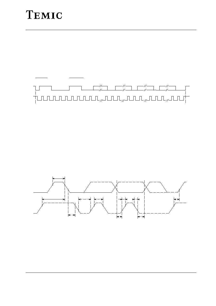
Bus Timing
SDA
SCL
t
t
t
t
t
t
t
t
t
t
R
F
S STO
H DAT
S DAT
HIGH
LOW
S STA
W STA
H STA
START
CLOCK
DATACHANGE
STOP
95 10725
Figure 3.
t
S STA
≠ Set ≠ up time start
t
W STA
≠ Waiting time start
t
H STA
≠ Hold time start
t
LOW
≠ "L" ≠ Pulse width clock
t
HIGH
≠ "H" ≠ Pulse width clock
t
S DAT
≠ Set ≠ up time data
t
H DAT
≠ Hold time data
t
S STO
≠ Set ≠ up time stop
t
R
≠ Rise time
t
F
≠ Fall time