U6239B
TELEFUNKEN Semiconductors
Rev. A3, 28-May-97
1 (15)
2.9 GHz PLL for SAT TV Tuner with UNi-Bus
Description
The U6239B is a single-chip frequency synthesizer with
bidirectional I
2
C bus control and unidirectional 3-wire
bus control, developed for SAT TV-tuner and cable tuner
applications.
This IC contains an integrated preamplifier, a high
frequency prescaler, a reference divider with multiple
programmable divider ratios, a crystal oscillator, a phase/
frequency detector together with a charge pump, a tuning
amplifier and an analog-to-digital converter.
Features
D 2.9 GHz divide-by-16 prescaler integrated
D UNi-BUS:
I
2
C bus and 3-wire bus
I
2
C bus software compatible to U6223B
3-wire bus software compatible to LC7215 (Sanyo)
D I
2
C bus mode:
4 bidirectional ports (open collector)
2 unidirectional ports (open collector)
5 level ADC or unidirectional port (open collector)
Address mode select function (AMS, Pin 3):
3 or 4 addresses selectable via Pin 10
D 3-wire bus mode:
4 unidirectional ports (open collector)
Lock output (open collector)
D Programmable reference divider
D Low power consumption (typ. 5 V / 23 mA)
D Electrostatic protection according to MIL-STD 883
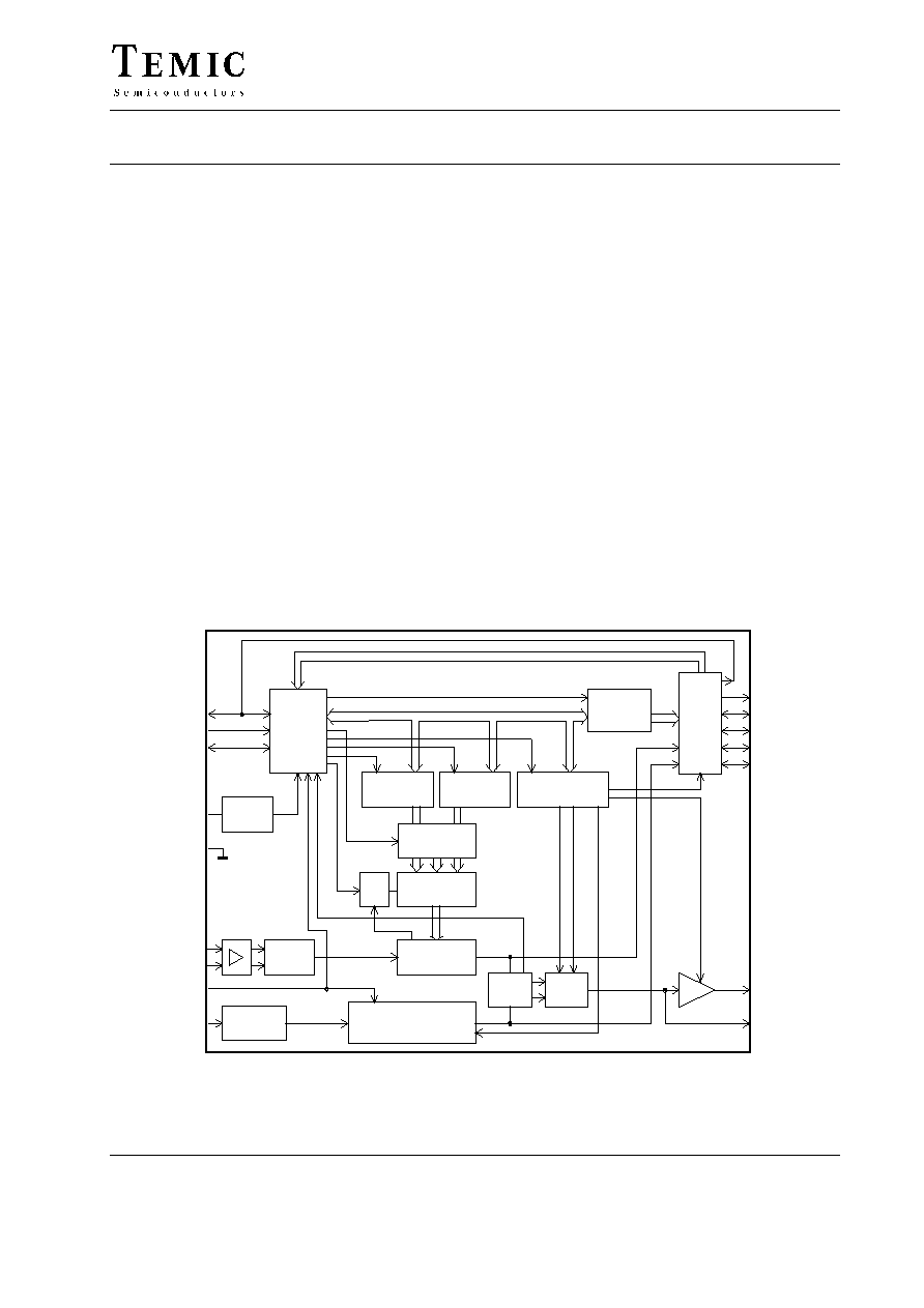
Block Diagram
ADC
AS / ENABLE / P3
5
10
5≠bit Latch
11
9
8
P7
P6 / ADC
P5
7
6
P4
I/O
Ports
7≠bit Latch
T1
8≠bit Latch
7≠bit Latch
SCL
SDA 4
12
Vs
OS
T0
5I
2
3
Oscillator
XTAL
divide by 256/512/off/1024
Phase
detector
Charge
pump
16 VD
1 PD
GND 15
Control
UNI≠BUS
FP
FR
15/14≠bit
Power≠on
reset
POR
P0/Lock
RD1,2,3
RDS / AMS
RFi
14
13
div. by 16
Prescaler
divide by 25/50/140/250
divide by 50/100/280/500
AMS
RDS
14≠bit Shift Reg.
Sync
LOCK
15≠bit Latch
SET
Sync
9611809
counter
Figure 1.
U6239B
TELEFUNKEN Semiconductors
Rev. A3, 28-May-97
2 (15)
Ordering Information
Extended Type Number
Package
Remarks
U6239B-AFPG3
SO16, plastic package
Taped and reeled
SSO16 package on request
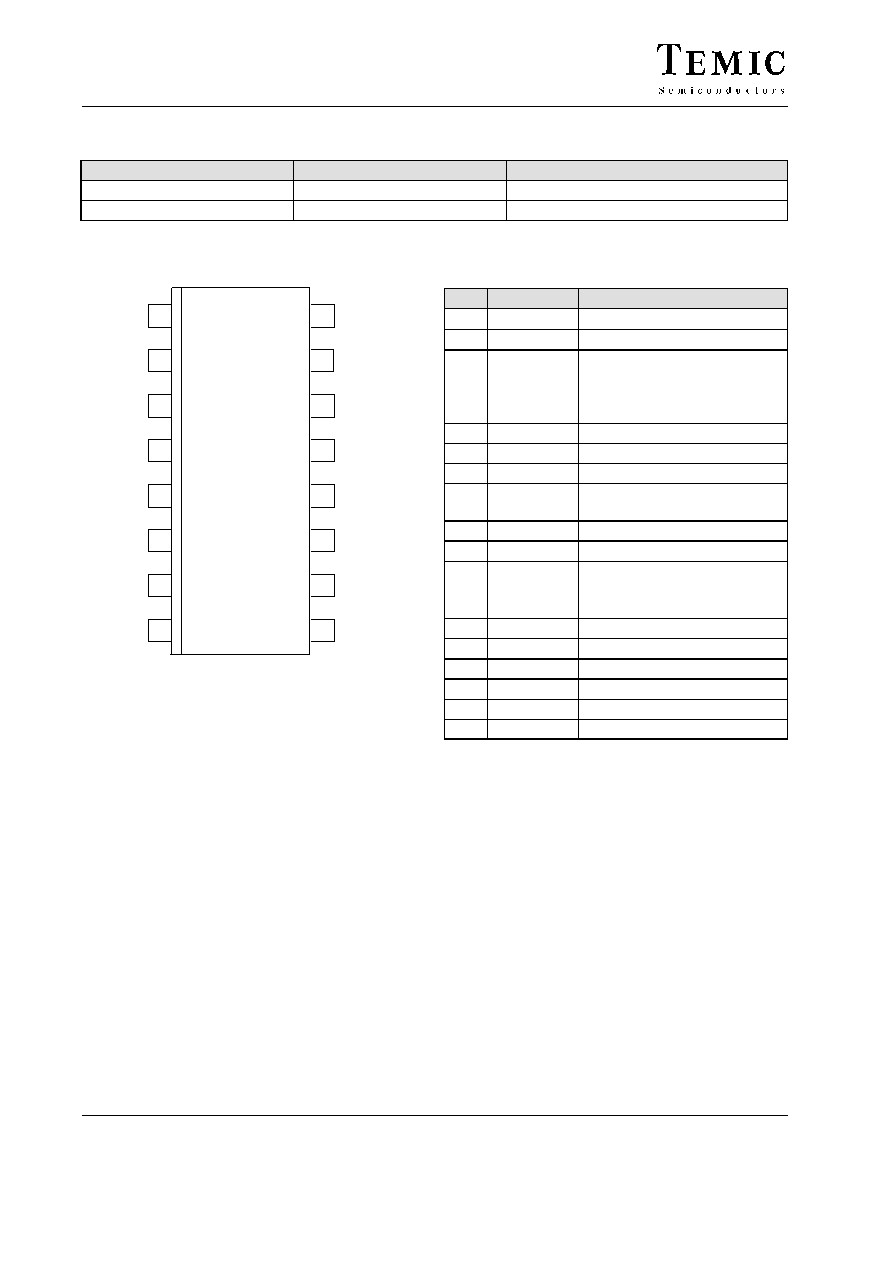
Pin Configuration
1
2
3
4
5
6
7
8
16
15
14
13
12
11
10
9
RDS/AMS
SDA
95 10947
SCL
P7
P6/ ADC
P5
PD
Q1
RFi
RFi
V
S
P0/ Lock
AS/ENABLE/
P3
P4
VD
GND
Pin
Symbol
Function
¡¡¡
¡¡¡
1
¡¡¡¡¡
¡¡¡¡¡
PD
¡¡¡¡¡¡¡¡¡¡
¡¡¡¡¡¡¡¡¡¡
Charge pump output
¡¡¡
¡¡¡
2
¡¡¡¡¡
¡¡¡¡¡
Q1
¡¡¡¡¡¡¡¡¡¡
¡¡¡¡¡¡¡¡¡¡
Crystal input
3
RDS/
AMS
Reference divider select input
(3-wire bus mode)
Address mode select input
(I
2
C bus mode)
¡¡¡
¡¡¡
4
¡¡¡¡¡
¡¡¡¡¡
SDA
¡¡¡¡¡¡¡¡¡¡
¡¡¡¡¡¡¡¡¡¡
Data input/ output
¡¡¡
¡¡¡
5
¡¡¡¡¡
¡¡¡¡¡
SCL
¡¡¡¡¡¡¡¡¡¡
¡¡¡¡¡¡¡¡¡¡
Clock input
¡¡¡
6
¡¡¡¡¡
P7
¡¡¡¡¡¡¡¡¡¡
Port 7 input/ output
¡¡¡
¡
¡
¡
¡¡¡
7
¡¡¡¡¡
¡
¡¡¡
¡
¡¡¡¡¡
P6/
ADC
¡¡¡¡¡¡¡¡¡¡
¡
¡¡¡¡¡¡¡¡
¡
¡¡¡¡¡¡¡¡¡¡
Port 6 output
Analog-Digital-Converter input
¡¡¡
¡¡¡
8
¡¡¡¡¡
¡¡¡¡¡
P5
¡¡¡¡¡¡¡¡¡¡
¡¡¡¡¡¡¡¡¡¡
Port 5 input/ output
¡¡¡
¡¡¡
9
¡¡¡¡¡
¡¡¡¡¡
P4
¡¡¡¡¡¡¡¡¡¡
¡¡¡¡¡¡¡¡¡¡
Port 4 input/ output
¡¡¡
¡
¡
¡
¡¡¡
10
¡¡¡¡¡
¡
¡¡¡
¡
¡¡¡¡¡
AS/
ENABLE/
P3
¡¡¡¡¡¡¡¡¡¡
¡
¡¡¡¡¡¡¡¡
¡
¡¡¡¡¡¡¡¡¡¡
Address select input
Enable input
Port 3 output
¡¡¡
¡¡¡
11
¡¡¡¡¡
¡¡¡¡¡
P0/Lock
¡¡¡¡¡¡¡¡¡¡
¡¡¡¡¡¡¡¡¡¡
Port 0 output/Lock output
¡¡¡
¡¡¡
12
¡¡¡¡¡
¡¡¡¡¡
V
S
¡¡¡¡¡¡¡¡¡¡
¡¡¡¡¡¡¡¡¡¡
Supply voltage
¡¡¡
¡¡¡
13
¡¡¡¡¡
¡¡¡¡¡
RFi
¡¡¡¡¡¡¡¡¡¡
¡¡¡¡¡¡¡¡¡¡
RF input
¡¡¡
¡¡¡
14
¡¡¡¡¡
¡¡¡¡¡
RFi
¡¡¡¡¡¡¡¡¡¡
¡¡¡¡¡¡¡¡¡¡
RF input
¡¡¡
¡¡¡
15
¡¡¡¡¡
¡¡¡¡¡
GND
¡¡¡¡¡¡¡¡¡¡
¡¡¡¡¡¡¡¡¡¡
Ground
¡¡¡
¡¡¡
16
¡¡¡¡¡
¡¡¡¡¡
VD
¡¡¡¡¡¡¡¡¡¡
¡¡¡¡¡¡¡¡¡¡
Active filter output
Circuit Description
The U6239B is a single-chip PLL designed for SAT TV
tuner and cable tuner. It consists of a divide-by-16
prescaler with an integrated preamplifier, a 15-bit
programmable divider, a crystal oscillator, and a
reference divider with selectable divider ratios, a phase/
frequency detector together with a charge pump which
drives the tuning amplifier. Only one external transistor
is required for varactor line driving. The device can be
controlled via I
2
C bus format or via 3-wire bus format. It
detects automatically which bus format has been
received. Therefore, there is no need for a bus selection
pin. In I
2
C bus mode, the device has four programmable
or one fixed and three programmable I
2
C bus addresses,
depending on the voltage level at Pin 3. They are
programmed by applying a specific input voltage to the
address select input Pin 10, enabling the use of up to four
synthesizers in a system. If the fixed address is used, this
pin can be used as a normal output port. The same pin
serves as the enable signal input in 3-wire bus mode.
Depending whether the fixed address is used or not there
are five or six open collector outputs for switching
functions available. In 3-wire bus mode there are four
open collector outputs and one lock signal output. All
open collector outputs are capable of sinking at least
10 mA. In I
2
C bus mode an analog-to-digital converter
(ADC) is available for digital AFC (automatic frequency
control) applications and the ports P4, P5 and P7 can also
be used as input ports.

U6239B
TELEFUNKEN Semiconductors
Rev. A3, 28-May-97
3 (15)
Functional Description
The U6239B is programmed via a 2-wire I
2
C bus or
3-wire bus depending on the received data format. In
I
2
C bus mode the three bus input pins 4, 5, 10 are used as
SDA, SCL and address select inputs or in 3-wire bus
mode as date, clock and enable inputs, respectively. The
data include the scaling factor SF and port output
information. In I
2
C bus mode there are some additional
functions available (ADC, bidirectional ports, etc.)
Oscillator frequency calculation :
f
VCO
= 16
SPF f
refosc
/SRF
f
vco
:
Locked frequency of voltage controlled oscillator
SPF : Scaling factor of programmable divider (15 bit in
I
2
C bus mode, 14 bit in 3-wire bus mode)
SRF : Scaling factor of reference divider
(
B25/B50/B140/B250/B256/B512/B1024
in I
2
C bus mode,
B25/B50/B100/B140/B250
B280/B500 in 3-wire bus mode)
f
refosc
: Reference oscillator frequency:
3.2/ 4 MHz crystal or external reference
frequency (max. 8 MHz)
The input amplifier together with a divide-by-16
prescaler provides excellent sensitivity (see "Typical
prescaler input sensitivity"). The input impedance is
shown in the diagram "Typical input impedance". When
a new divider ratio is entered according to the requested
f
VCO
, the phase detector and charge pump adjusts the
control voltage of the VCO together with the tuning
amplifier until the output signals of the programmable
divider and the reference divider are in frequency locked
and phase locked. The reference frequency may be pro-
vided by an external source, capacitively coupled into
Pin 2, or by using an on-board crystal with an 18 pF ca-
pacitor in series. The crystal operates in the series
resonance mode. The reference divider division ratio
is selectable to
B25/ B50/ B140/ B250/ B256/ B512/
B1024 in the I
2
C bus mode and
B25/ B50/ B100/
B140/ B250/ B280/ B500 in the 3-wire bus mode.
In I
2
C bus mode, the division ratio may be set via three
bits, in 3-wire bus mode via two bits and a voltage at the
reference divider select input Pin 3. In addition, there are
port outputs available for band switching and other
purposes.
Application
A typical application is shown on page 14. All input/
output interface circuits are shown on the pages 12 and
13. Some special features which are related to test- and
alignment procedures for tuner production are explained
together with the bus mode descriptions.
Absolute Maximum Ratings
All voltages are referred to GND (Pin 15)
Parameters
Symbol
Conditions
Min.
Max.
Unit
¡¡¡¡¡¡¡¡¡¡¡¡¡¡
¡¡¡¡¡¡¡¡¡¡¡¡¡¡
Supply voltage
Pin 12
¡¡¡¡
¡¡¡¡
Vs
¡¡¡¡¡¡
¡¡¡¡¡¡
¡¡¡¡
¡¡¡¡
≠0.3
¡¡¡¡¡
¡¡¡¡¡
6
¡¡¡¡
¡¡¡¡
V
¡¡¡¡¡¡¡¡¡¡¡¡¡¡
¡¡¡¡¡¡¡¡¡¡¡¡¡¡
RF input voltage
Pins 13, 14
¡¡¡¡
¡¡¡¡
RFi
¡¡¡¡¡¡
¡¡¡¡¡¡
¡¡¡¡
¡¡¡¡
≠0.3
¡¡¡¡¡
¡¡¡¡¡
Vs + 0.3
¡¡¡¡
¡¡¡¡
V
¡¡¡¡¡¡¡¡¡¡¡¡¡¡
¡¡¡¡¡¡¡¡¡¡¡¡¡¡
Port output current
Pins 6-11
¡¡¡¡
¡¡¡¡
P0, P3-7
¡¡¡¡¡¡
¡¡¡¡¡¡
Open collector
¡¡¡¡
¡¡¡¡
≠1
¡¡¡¡¡
¡¡¡¡¡
15
¡¡¡¡
¡¡¡¡
mA
¡¡¡¡¡¡¡¡¡¡¡¡¡¡
¡¡¡¡¡¡¡¡¡¡¡¡¡¡
Total port output current
Pins 6-11
¡¡¡¡
¡¡¡¡
P0, P3-7
¡¡¡¡¡¡
¡¡¡¡¡¡
Open collector
¡¡¡¡
¡¡¡¡
≠1
¡¡¡¡¡
¡¡¡¡¡
50
¡¡¡¡
¡¡¡¡
mA
¡¡¡¡¡¡¡¡¡¡¡¡¡¡
¡¡¡¡¡¡¡¡¡¡¡¡¡¡
Port input/ output voltage
Pins 6-10
¡¡¡¡
¡¡¡¡
P3-7
¡¡¡¡¡¡
¡¡¡¡¡¡
In off state
¡¡¡¡
¡¡¡¡
≠0.3
¡¡¡¡¡
¡¡¡¡¡
14
¡¡¡¡
¡¡¡¡
V
¡¡¡¡¡¡¡¡¡¡¡¡¡¡
Port output voltage
Pins 6-11
¡¡¡¡
P0, P3-7
¡¡¡¡¡¡
In on state
¡¡¡¡
≠0.3
¡¡¡¡¡
6
¡¡¡¡
V
¡¡¡¡¡¡¡¡¡¡¡¡¡¡
¡
¡¡¡¡¡¡¡¡¡¡¡¡
¡
¡¡¡¡¡¡¡¡¡¡¡¡¡¡
Bus input/ output voltage
Pins 4 and 5
¡¡¡¡
¡
¡¡
¡
¡¡¡¡
VSDA,
VSCL
¡¡¡¡¡¡
¡
¡¡¡¡
¡
¡¡¡¡¡¡
¡¡¡¡
¡
¡¡
¡
¡¡¡¡
≠0.3
¡¡¡¡¡
¡
¡¡¡
¡
¡¡¡¡¡
6
¡¡¡¡
¡
¡¡
¡
¡¡¡¡
V
¡¡¡¡¡¡¡¡¡¡¡¡¡¡
¡¡¡¡¡¡¡¡¡¡¡¡¡¡
SDA output current
Pin 4
¡¡¡¡
¡¡¡¡
ISDA
¡¡¡¡¡¡
¡¡¡¡¡¡
Open collector
¡¡¡¡
¡¡¡¡
≠1
¡¡¡¡¡
¡¡¡¡¡
5
¡¡¡¡
¡¡¡¡
mA
¡¡¡¡¡¡¡¡¡¡¡¡¡¡
¡
¡¡¡¡¡¡¡¡¡¡¡¡
¡
¡¡¡¡¡¡¡¡¡¡¡¡¡¡
Address select/ Enable input Pin 10
Port output voltage
¡¡¡¡
¡
¡¡
¡
¡¡¡¡
AS/
ENABLE/
P3
¡¡¡¡¡¡
¡
¡¡¡¡
¡
¡¡¡¡¡¡
Port in off
state
¡¡¡¡
¡
¡¡
¡
¡¡¡¡
≠0.3
¡¡¡¡¡
¡
¡¡¡
¡
¡¡¡¡¡
14
¡¡¡¡
¡
¡¡
¡
¡¡¡¡
V
¡¡¡¡¡¡¡¡¡¡¡¡¡¡
¡¡¡¡¡¡¡¡¡¡¡¡¡¡
Charge pump output voltage Pin 1
¡¡¡¡
¡¡¡¡
PD
¡¡¡¡¡¡
¡¡¡¡¡¡
¡¡¡¡
¡¡¡¡
≠0.3
¡¡¡¡¡
¡¡¡¡¡
Vs + 0.3
¡¡¡¡
¡¡¡¡
V
¡¡¡¡¡¡¡¡¡¡¡¡¡¡
¡¡¡¡¡¡¡¡¡¡¡¡¡¡
Active filter output voltage Pin 16
¡¡¡¡
¡¡¡¡
VD
¡¡¡¡¡¡
¡¡¡¡¡¡
¡¡¡¡
¡¡¡¡
≠0.3
¡¡¡¡¡
¡¡¡¡¡
Vs + 0.3
¡¡¡¡
¡¡¡¡
V
¡¡¡¡¡¡¡¡¡¡¡¡¡¡
¡¡¡¡¡¡¡¡¡¡¡¡¡¡
Crystal oscillator voltage
Pin 2
¡¡¡¡
¡¡¡¡
Q1
¡¡¡¡¡¡
¡¡¡¡¡¡
¡¡¡¡
¡¡¡¡
≠0.3
¡¡¡¡¡
¡¡¡¡¡
Vs + 0.3
¡¡¡¡
¡¡¡¡
V
Reference divider select input/ Pin 3
Address mode select input
RDS/
AMS
≠0.3
V
S
+ 0.3
V
Junction temperature
T
j
≠40
125
∞
C
Storage temperature
T
stg
≠40
125
∞
C

U6239B
TELEFUNKEN Semiconductors
Rev. A3, 28-May-97
4 (15)
Operating Range
All voltages are referred to GND (Pin 15)
Parameters
Test Conditions / Pins
Symbol
Min.
Typ.
Max.
Unit
¡¡¡¡¡¡¡¡¡
¡¡¡¡¡¡¡¡¡
Supply voltage
¡¡¡¡¡¡¡¡¡
¡¡¡¡¡¡¡¡¡
Pin 12
¡¡¡¡
¡¡¡¡
V
S
¡¡¡¡
¡¡¡¡
4.5
¡¡¡¡
¡¡¡¡
5
¡¡¡¡
¡¡¡¡
5.5
¡¡¡¡
¡¡¡¡
V
¡¡¡¡¡¡¡¡¡
¡¡¡¡¡¡¡¡¡
Ambient temperature
¡¡¡¡¡¡¡¡¡
¡¡¡¡¡¡¡¡¡
¡¡¡¡
¡¡¡¡
T
amb
¡¡¡¡
¡¡¡¡
≠20
¡¡¡¡
¡¡¡¡
¡¡¡¡
¡¡¡¡
85
¡¡¡¡
¡¡¡¡
∞
C
¡¡¡¡¡¡¡¡¡
¡¡¡¡¡¡¡¡¡
Input frequency
¡¡¡¡¡¡¡¡¡
¡¡¡¡¡¡¡¡¡
Pins 13 and 14
¡¡¡¡
¡¡¡¡
RFi
¡¡¡¡
¡¡¡¡
250
¡¡¡¡
¡¡¡¡
¡¡¡¡
¡¡¡¡
2900
¡¡¡¡
¡¡¡¡
MHz
¡¡¡¡¡¡¡¡¡
¡¡¡¡¡¡¡¡¡
Programmable divider
¡¡¡¡¡¡¡¡¡
¡¡¡¡¡¡¡¡¡
I
2
C bus mode
¡¡¡¡
¡¡¡¡
SF
¡¡¡¡
¡¡¡¡
256
¡¡¡¡
¡¡¡¡
¡¡¡¡
¡¡¡¡
32767
¡¡¡¡
¡¡¡¡
¡¡¡¡¡¡¡¡¡
¡¡¡¡¡¡¡¡¡
Programmable divider
¡¡¡¡¡¡¡¡¡
¡¡¡¡¡¡¡¡¡
3-wire bus mode
¡¡¡¡
¡¡¡¡
SF
¡¡¡¡
¡¡¡¡
256
¡¡¡¡
¡¡¡¡
¡¡¡¡
¡¡¡¡
16383
¡¡¡¡
¡¡¡¡
Thermal Resistance
Parameters
Test Conditions / Pins
Symbol
Min.
Typ.
Max.
Unit
Junction ambient
Package SO16 soldered to PCB
R
thJA
110
K/W
Electrical Characteristics
Test conditions (unless otherwise specified): V
S
= 5 V, T
amb
= 25
∞
C
Parameters
Test Conditions / Pins
Symbol
Min.
Typ.
Max.
Unit
¡¡¡¡¡¡¡¡¡¡
¡¡¡¡¡¡¡¡¡¡
Supply current (prescaler on)
¡¡¡¡¡¡¡¡¡
¡¡¡¡¡¡¡¡¡
Ports off
Pin 12
¡¡¡¡¡
¡¡¡¡¡
ICC
¡¡¡
¡¡¡
¡¡¡¡
¡¡¡¡
23
¡¡¡
¡¡¡
¡¡¡¡
¡¡¡¡
mA
¡¡¡¡¡¡¡¡¡¡¡¡¡¡¡¡¡¡¡¡¡¡¡¡¡¡¡¡¡¡¡¡
¡¡¡¡¡¡¡¡¡¡¡¡¡¡¡¡¡¡¡¡¡¡¡¡¡¡¡¡¡¡¡¡
Input sensitivity
¡¡¡¡¡¡¡¡¡¡
¡¡¡¡¡¡¡¡¡¡
f
RFi
= 250 MHz
¡¡¡¡¡¡¡¡¡
¡¡¡¡¡¡¡¡¡
Pin 13
¡¡¡¡¡
¡¡¡¡¡
Vi
1
)
¡¡¡
¡¡¡
100
¡¡¡¡
¡¡¡¡
¡¡¡
¡¡¡
300
¡¡¡¡
¡¡¡¡
mV
rms
¡¡¡¡¡¡¡¡¡¡
¡¡¡¡¡¡¡¡¡¡
f
RFi
= 750 -2900 MHz
¡¡¡¡¡¡¡¡¡
¡¡¡¡¡¡¡¡¡
Pin 13
¡¡¡¡¡
¡¡¡¡¡
Vi
1
)
¡¡¡
¡¡¡
20
¡¡¡¡
¡¡¡¡
¡¡¡
¡¡¡
300
¡¡¡¡
¡¡¡¡
mV
rms
¡¡¡¡¡¡¡¡¡¡¡¡¡¡¡¡¡¡¡¡¡¡¡¡¡¡¡¡¡¡¡¡
¡¡¡¡¡¡¡¡¡¡¡¡¡¡¡¡¡¡¡¡¡¡¡¡¡¡¡¡¡¡¡¡
Crystal oscillator
¡¡¡¡¡¡¡¡¡¡
¡
¡¡¡¡¡¡¡¡
¡
¡¡¡¡¡¡¡¡¡¡
Recommended crystal series
resistance
¡¡¡¡¡¡¡¡¡
¡
¡¡¡¡¡¡¡
¡
¡¡¡¡¡¡¡¡¡
¡¡¡¡¡
¡
¡¡¡
¡
¡¡¡¡¡
¡¡¡
¡
¡¡
¡¡¡
10
¡¡¡¡
¡
¡¡
¡
¡¡¡¡
¡¡¡
¡
¡
¡
¡¡¡
200
¡¡¡¡
¡
¡¡
¡
¡¡¡¡
W
¡¡¡¡¡¡¡¡¡¡
¡¡¡¡¡¡¡¡¡¡
Crystal oscillator drive level
¡¡¡¡¡¡¡¡¡
¡¡¡¡¡¡¡¡¡
Pin 2
¡¡¡¡¡
¡¡¡¡¡
¡¡¡
¡¡¡
¡¡¡¡
¡¡¡¡
50
¡¡¡
¡¡¡
¡¡¡¡
¡¡¡¡
mV
rms
¡¡¡¡¡¡¡¡¡¡
¡
¡¡¡¡¡¡¡¡
¡
¡¡¡¡¡¡¡¡¡¡
Crystal oscillator source
impedance
¡¡¡¡¡¡¡¡¡
¡
¡¡¡¡¡¡¡
¡
¡¡¡¡¡¡¡¡¡
Nominal spread
" 15%
Pin 2
¡¡¡¡¡
¡
¡¡¡
¡
¡¡¡¡¡
¡¡¡
¡
¡¡
¡¡¡
¡¡¡¡
¡
¡¡
¡
¡¡¡¡
≠650
¡¡¡
¡
¡
¡
¡¡¡
¡¡¡¡
¡
¡¡
¡
¡¡¡¡
W
¡¡¡¡¡¡¡¡¡¡
¡¡¡¡¡¡¡¡¡¡
External reference input
frequency
¡¡¡¡¡¡¡¡¡
¡¡¡¡¡¡¡¡¡
AC coupled sinewave
Pin 2
¡¡¡¡¡
¡¡¡¡¡
¡¡¡
¡¡¡
2
¡¡¡¡
¡¡¡¡
¡¡¡
¡¡¡
8
¡¡¡¡
¡¡¡¡
MHz
¡¡¡¡¡¡¡¡¡¡
¡
¡¡¡¡¡¡¡¡
¡
¡¡¡¡¡¡¡¡¡¡
External reference input
amplitude
¡¡¡¡¡¡¡¡¡
¡
¡¡¡¡¡¡¡
¡
¡¡¡¡¡¡¡¡¡
AC coupled sinewave
Pin2
¡¡¡¡¡
¡
¡¡¡
¡
¡¡¡¡¡
¡¡¡
¡
¡¡
¡¡¡
70
¡¡¡¡
¡
¡¡
¡
¡¡¡¡
¡¡¡
¡
¡
¡
¡¡¡
200
¡¡¡¡
¡
¡¡
¡
¡¡¡¡
mV
rms
Port outputs (current limited, output function only in I
2
C bus mode)
Port P0 at Pin 11.
Port P3 at Pin 10, is only usable with AMS = `L' (= 3 address mode).
P0, P3 Sink current
VH = 12 V, Pins 10 and 11
ISL
0.7
1
1.5
mA
Leakage current
VH = 13.2 V
IL
10
mA
Port outputs, Lock output (open collector, locked = `L'. Ports P4 ≠ P7 at Pins 6≠9)
Lock output at Pin 11, only in 3-wire bus mode.
Saturation voltage
IL = 10 mA
VSL
2
)
0.5
V
Leakage current
VH = 13.2 V
IL
10
mA
Port inputs (Ports 4, 5 and 7 at Pins 6, 8 and 9)
Input voltage high
Vi `H'
2.7
V
Input voltage low
Vi `L'
0.8
V
Input current high
Vi `H' = 13.2 V
Ii `H'
10
mA
Input current low
Vi `L' = 0 V
Ii `L'
≠10
mA
U6239B
TELEFUNKEN Semiconductors
Rev. A3, 28-May-97
5 (15)
Electrical Characteristics (continued)
Parameters
Test Conditions / Pins
Symbol
Min.
Typ.
Max.
Unit
ADC input (ADC, Pin 7, see page 8 for ADC-levels)
Input current high
Vi `H' = 13.2 V
Ii `H'
10
mA
Input current low
Vi `L' = 0 V
Ii `L'
≠10
mA
Charge pump output (PD)
Charge pump current `H'
5I = 1, VPD = 1.7 V, Pin 1
IPDH
"180
mA
Charge pump current `L'
5I = 0, VPD = 1.7 V, Pin 1
IPDL
"50
mA
Charge pump leakage current
T0 = 1, VPD = 1.7 V, Pin 1
IPDTRI
"5
nA
Charge pump amplifier gain
Pins 1 and 16
6400
Bus inputs Data and Clock (SDA, SCL) I
2
C bus mode and 3-wire bus mode
Input voltage high
Pins 4 and 5
Vi `H'
3
5.5
V
Input voltage low
Pins 4 and 5
Vi `L'
1.5
V
Input current high
Vi `H' = V
S
, Pins 4 and 5
Ii `H'
10
mA
Input current low
Vi `L' = 0 V, Pins 4 and 5
Ii `L'
≠20
mA
Output voltage SDA
(open collector)
ISDA`L' = 3 mA, Pin 4
VSDA `L'
0.4
V
Bus input Enable, 3-wire bus mode (ENABLE, Pin 10)
Input voltage high
Pin 10
Vi `H'
75%
V
S
V
S
+
0.3 V
V
Input voltage low
Pin 10
Vi `L'
1.0
V
Input current high
Vi `H' = V
S
, Pin 10
Ii `H'
10
mA
Input current low (RDS = `L')
Vi `L' = 0 V, Pin 10
Ii `L'
≠10
mA
Input current low (RDS = `H')
Vi `L' = 0 V, Pin 10
Ii `L'
≠100
mA
Address selection / port output (AS/P3, Pin 10)
Input current low (AMS = L)
Vi `L' = 0 V (3 address)
Ii `L'
≠10
mA
Input current high (AMS = L)
Vi `H' = 13.2 V (3 address)
Ii `H'
10
mA
Input current low (AMS = H)
Vi `L' = 0 V (4 address)
Ii `L'
≠100
mA
Input current high (AMS = H)
Vi `H' = V
S
(4 address)
Ii `H'
10
mA
Reference divider select/Address mode select (RDS, AMS)
Input voltage high
Pins 4 and 5
Vi `H'
3
5.5
V
Input voltage low
Pins 4 and 5
Vi `L'
1.5
V
Input current high
Vi `H' = V
S
, Pins 4 and 5
Ii `H'
10
mA
Input current low
Vi `L' = 0 V, Pins 4 and 5
Ii `L'
≠20
mA
Notes:
1
) RMS - voltage calculated from the measured available power on 50
W.
2
) Tested with one port active. The collector voltage of an active port must not exceed 6 V.