
U6268B
Preliminary Information
TELEFUNKEN Semiconductors
Rev. A1, 21-May-97
1 (12)
Side-Airbag Sensor Dual Interface
Description
The U6268B is an interface IC for remote automotive
sensors. It links the crash sensors in the driver- and
passenger door with the main airbag unit in the
dashboard. Two identical channels supply the external
sensors and receive digital information from them via one
active wire each. The interface supplies the external
sensors with a pre-regulated smoothed voltage, the
external units transmit the digital information back to the
interface by current modulation.
As the device is for safety critical applications, highest
data transmission security is mandatory. With high
immunity against cross-coupling between the two
channels, the U6228B is tailored for the harsh automotive
environment.
Features
D Two identical interface channels
D Provides a pre-regulated smoothed voltage and a
supply current up to 50 mA for the sensors
D Receives data from the sensors by current modulation
with a transmission rate of 60 kBaud (transmission
bandwidth 500 kHz)
D Current modulation provides high noise immunity for
data transfer
D TTL-compatible input activate the sensor
D Data output can be directly connected to a micro-
controller input
D Operation supply voltage range 5.7 V v V
S
v 40 V
D ESD protection according to MIL-STD-883C test
method 3015.7
D High-level EMI protection
Benefits
D Voltage supply and data transmission with one active
wire over long distances
Ordering Information
Extended Type Number
Package
Remarks
U6268B
SO16
Block Diagram
Short circuit
detection
Temperature
monitor
Smoothed voltage
regulator
I/U converter
Smoothed voltage
regulator
I/U converter
Voltage
comparator
Channel 1
Data
Enable
Enable
Voltage
comparator
Channel 2
Data
Crash
sensor
Channel 1
Channel 2
Channel 1
power
supply
Data
trans�
mission
Crash
sensor
Channel 2
power
supply
Data
trans�
mission
13839
�
C
Figure 1. Block diagram

U6268B
TELEFUNKEN Semiconductors
Rev. A1, 21-May-97
Preliminary Information
2 (12)
Pin Description
V
S
OUT1
OUT2
SC
RETURN2
GND
GND
RETURN1
1
2
3
4
5
6
7
8
16
15
14
13
12
11
10
9
13321
CLL1
OCM1
OCM2
CLL2
ENABLE2
GND
GND
ENABLE1
Figure 2. Pinning
Pin
Symbol
Function
1
GND
Ground and reference pin
2
RETURN1
Return line of the external unit,
internally connected to GND via
a line-protection transistor
3
OUT1
Voltage-stabilized supply output
and current-modulation input
4
V
S
Supply voltage of the IC
5
OUT2
Voltage stabilized supply output
and current modulation input
6
SC
Smooth time constant for slow
voltage change at both OUT
pins
7
RETURN2
Return line of the external unit,
internally connected to GND via
a line-protection transistor
8, 9
GND
Ground and reference pin
10
ENABLE1
Controls OUT1 voltage,
ENABLE1 High means OUT1
active, ENABLE1 Low or open
means OUT1 switched off
11
CLL2
Current logic level output, low
at high OUT2 current,
monitoring via OCM2
12
OCM2
Analog current output, repre-
senting 1/10 current of OUT2
13
OCM1
Analog current output, repre-
senting 1/10 current of OUT1
14
CLL1
Current logic level output, low
at high OUT1 current, moni-
toring via OCM1
15
ENABLE2
Controls OUT2 voltage,
ENABLE2 High means OUT2
active, ENABLE1 Low or open
means OUT2 switched off
16
GND
Ground and reference pin
Figure 3. Application circuit
Functional Description
V
S
The IC and the external units are powered via the V
S
Pin 4. This pin is connected to the battery via a reverse
battery protection diode. An electrolythic capacitor of
22
mF smoothes the voltage and absorbes positive and
negative transients.
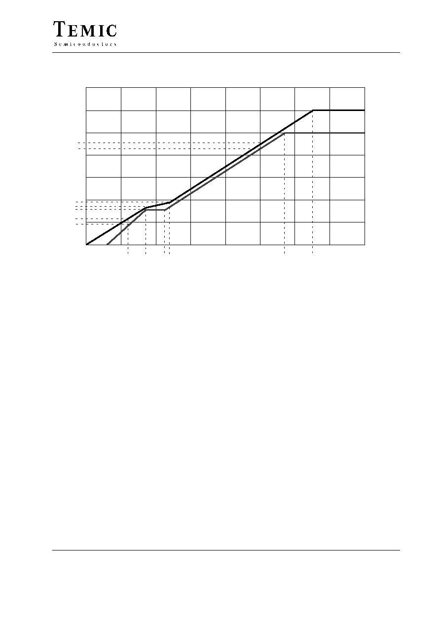
OUT1, OUT2
OUTx provides a smoothed, very slowly changing supply
voltage for the external units and monitors the output cur-
rent. During normal operating conditions, the OUTx
voltage is typ. 3 V below V
S
, and changes very slowly
with a varying battery voltage in order to suppress distur-
bances in the data transmission. At low V
S
(5.7 to 8.5 V),
the OUTx voltage is typ. 0.5 V below V
S
. This voltage
difference is reduced in order to ensure sufficient supply
voltage for the external unit between OUTx and
RETURNx. The output current capability is 50 mA. The
internal pull-down current at OUTx is typically 3 mA.
U6268B
Preliminary Information
TELEFUNKEN Semiconductors
Rev. A1, 21-May-97
3 (12)
0
5
10
15
20
25
30
35
0
5
10
15
20
25
30
35
40
V
S
( V )
13322
out
22.4
21.4
9.4
8.2
5.4
4.9
7.7
5.7
8.5
11.3 12.0
28.6
32.6
Vout max
Vout min
V
(
V
)
Figure 4. Output voltage with tolerances vs. supply voltage
The data transmission from the external unit to the
interface IC is carried out on the same line by varying the
current level. The quiescent current consumption of the
external unit is about 5 to 15 mA. This current level is
interpreted as logic high level at CLL-pin. The external
unit can switch on an additional current of 30 mA,
interpreted by the interface as logic low. The current
changes within approximately 1
ms, sufficient for a
transmission rate of about 60 kBaud, requiring a
transmission bandwidth of about 500 kHz for the current-
monitoring subcircuit and the OCM output. For a good
current transmission behaviour, the dynamic resistance of
OUTx may not exceed 12
W inside the bandwidth range
(total of 15
W for OUTx and RETURN).
The OUTx- voltage can be switched off by
ENABLEx = LOW to reset the external unit and to
reduce power dissipation during fault conditions.
The OUT pins are overtemperature- and short-circuit
protected. A reverse polarity diode at Pin V
S
(Pin 4) en-
sures that no current is fed back to the V
Batt
-system in the
case of a short between OUTx and V
Batt
. A minimum ca-
pacity of 33 nF is required at the pins OUTx .
ENABLE1, ENABLE2
ENABLEx is a microcontroller-compatible input which
switches the related output on or off.
D Low or open circuit applied to ENABLEx switches
the related OUTx and RETURNx off (high imped-
ance). A sink current at Pin OUTx discharges the
capacitive load.
D High applied to ENABLEx switches the related
OUTx and RETURNx on to supply the external unit.
OCM1, OCM2
The output current of OUTx is monitored with a transmis-
sion factor of 0.1 to the OCMx. With a resistor from OCM
to GND, the current is converted to a voltage. The electri-
cal characteristics are specified by R
OCM
= 750
W. The
CLL-current threshold, the OUT-current limitation and
the OUT-current detection can be changed by varying
R
OCM
in a range from 500
W to 1 kW.
The current monitoring enables to detect overcurrent
conditions at OUTx (short circuit to GND or RETURNx)
and to detect low current conditions at OUTx (short cir-
cuit to V
Batt
or open load).
The internal pull-down current at the OUTx creates no
OCMx-current. During enable, the minimum voltage at
OCMx is the saturation voltage of an internal NPN-tran-
sistor with typically 0.1 V. The maximum voltage at
OCM is limited by an internal clamping diode to 5.3 V.
CLL1, CLL2
The current at Pin OUTx is logical evaluated and ready
to use for a microcontroller input. With this stage, the

U6268B
TELEFUNKEN Semiconductors
Rev. A1, 21-May-97
Preliminary Information
4 (12)
logic data transmission from the external unit to the inter-
face is completed.
CLLx is the output stage of a comparator with an internal
threshold and with the OCMx input. A OCMx-voltage
higher than 2.4 V creates a logic low at CLLx, and a
OCMx-voltage lower than 1.43 V creates a logic high at
CLLx. The comparator has an internal hysteresis with
typically 0.4 V.
With the pull-down resistor R
OCMx
= 750
W at OCMx, the
correct OUTx-current threshold related to the logical out-
put CLLx is ensured. The CLLx is 'low' if the
OUTx-current is higher than 27.3 mA, and the CLLx is
'high', if the OUTx-current is lower than 19.1 mA. The
comparator has an internal hysteresis of typically 5 mA.
The tolerance of the R
OCM
resistor is assumed to be 0%.
The CLL-pin is an open-collector output and needs a
pull-up resistor of typically 2 k
W to the 5-V supply. For
ESD protection, a 7-V Zener diode is implemented.
RETURN 1, RETURN 2
The RETURNx pin provides a low-ohmic connection to
GND via a switched open-collector NPN-transistor. If
ENABLEx is high, RETURNx is switched on with a satu-
ration voltage less than 0.5 V at I
RETURNx
v 50 mA. If
ENABLEx is low or open, RETURNx is a current sink
with
v 2 mA. RETURNx is current-limited at typically
150 mA.
SC
The smooth capacitor is designed to realize the long-time
constant for the slow voltage change at OUTx for both in-
terface channels. The capacity is typ. 22 nF. At the rising
edge of V
Batt
, the maximum slew rate is V
OUTx
= 5 V/ms,
and at the falling edge of V
Batt
, the maximum slew rate
is V
OUTx
= 10 V/ms.
GND-Pins
By means of a GND bond from the chip to Pin 1 and Pin 8,
high ground breakage security is achieved and lowest
voltage drop and ground shift between IC- and circuit
ground is provided. The four GND pins and the die pad
are directly connected to the copper leadframe, resulting
in a very low thermal resistance, R
thJC
. In order to achieve
a good thermal resistance, R
thJA,
a good copper connec-
tion from the four GND pins to the metal parts of the
modul housing is also recommended.
Power Dissipation
Worst case calculation of the supply current I
S
:
I
S
= 1,278
( I
OUT1
+ I
OUT2
) + 18 mA
Worst case calculation of the IC's power dissipation P
V
:
P
V
= (V
S
I
S
) � [(V
S
� V
diff
� V
ret-sat
)
(I
OUT1
+ I
OUT2
)
+R
OCM
((I
OUT1
2
+ I
OUT2
2
) / 81)]
V
S
= supply voltage 5.7 to 25 V
voltage difference V
S
to V
OUTx
V
diff
= 3.6 at 12 V
vV
S
v 25 V
V
diff
= 0.8 at 5.7 V
vV
S
v 8.5 V
V
ret-sat
= 0.5 V saturation voltage return
I
OUTx
= output current at Pin OUTx = 0 to 60 mA
R
OCM
= resistor at Pin OCMx
Selective Overtemperature Protection
An overtemperature protection is integrated which gene-
rates a switch-off signal at a chip temperature of typically
T
j
= 160
�
C and a switch-on signal at typically T
j
= 150
�
C.
In case of a detected overtemperature, only the corre-
sponding channel is disabled. The other channel stays
enabled.
The RETURNx is switched off if the voltage at RE-
TURNx is higher than 2 V (short-circuit comparator
threshold) and overtemperature is detected.
The OUTx is switched off if the voltage at OCMx is
higher than 4.6 V (overcurrent detection level) and over-
temperature is detected. The OCM voltage monitors the
output current at OUTx via the current ratio of 0.1. The
overcurrent-detection level of OUTx can be varied by
changing the OCMx resistor. If OUTx is switched off by
overtemperature and overcurrent detection, the CLLx
output remains logic low (overcurrent).
As the IC is only overtemperature-protected for short-cir-
cuit conditions at RETURNx or OUTx, it has to be
checked in each application that the chip temperature
does not exceed T
jmax
= 150
�
C in normal operation.
Test Hint
The overtemperature signal can be activated by con-nect-
ing ENABLE1 or ENABLE2 to 9 V/ 10 mA.

U6268B
Preliminary Information
TELEFUNKEN Semiconductors
Rev. A1, 21-May-97
5 (12)
Absolute Maximum Ratings
Parameters
Symbol
Min.
Typ.
Max.
Unit
Supply voltage
V
S
�0.6
40
V
Voltage at pins CLL1, CLL2, ENABLE1, ENABLE2
�0.3
6
V
Voltage at SC
V
SC
�0.3
30
V
Voltage at OCM1, OCM2
V
OCMx
�0.3
6.8
V
Voltage at RETURN1, RETURN2
V
RETURNx
�1
27
V
Voltage at OUT1, OUT2
V
OUTx
�1
40
V
Current at supply
(both channels OUTx and RETURNx shorted)
I
S
240
mA
Current at logical pins: CLL1, CLL2
ENABLE1, ENABLE2
I
CCLx
I
ENABLEx
3
0.1
mA
mA
Current at SC (SC related to GND or V
Batt
)
I
SC
�110
220
mA
Current at pins to external unit
OUT1, OUT2, RETURN1, RETURN2
internal
limited
ESD classification
Human body model (100 pF, 1.5 k
W)
Machine model (200 pF, 0.0
W)
All pins
"2000
"200
V
V
Ambient temperature range
T
amb
�40
95
�
C
Junction temperature range
T
j
�40
150
�
C
Storage temperature range
T
stg
�55
125
�
C
Thermal Resistance
Parameters
Symbol
Value
Unit
Junction to pin
R
thJC
36
k/W
Junction ambient is reachable with a big pad size for
GND near a screw or the metal housing
R
thJA
65
k/W
Electrical Characteristics
T
amb
= �40 to 95
�
C and T
j
= �40 to 150
�
C,
operation supply voltage range 5.7 to 18 V continuously,
v25 V for max. 25 min, v40 V for up to 500 ms.
The current values are based on the 750
W 0% resistor at OCM1/OCM2
Parameters
Test Conditions / Pins
Symbol
Min.
Typ.
Max.
Unit
Supply current
T
125
�
C
Outputs disabled, V
S
v 18 V
I
S
8
mA
pp y
T
j
w 125
�
C
Outputs disabled, V
S
v 40 V
I
S
14
mA
One output enabled, V
S
v 18 V
I
S
13
mA
Both outputs enabled, V
S
v 18 V
I
S
18
mA
Output load 2
15 mA, V
S
v18 V
I
S
56
mA
Output load 2
28 mA, V
S
v18 V
I
S
90
mA
Output load 2
50 mA, V
S
v18 V
I
S
146
mA
Output load 2
60 mA,
V
S
v 18 V (T
j
> 125
�
C)
I
S
171
mA
Both channels OUTx and
RETURNx shorted, V
S
v 18 V
I
S
200
mA
Function SC

U6268B
TELEFUNKEN Semiconductors
Rev. A1, 21-May-97
Preliminary Information
6 (12)
Unit
Max.
Typ.
Min.
Symbol
Test Conditions / Pins
Parameters
Voltage at SC
V
S
= 5.7 V
V
SC
5.1
5.3
V
Voltage at SC
V
S
= 12.5 V
V
SC
9
9.4
V
Maximal voltage at SC
V
S
= 40 V
V
SCmax
30
V
SC-discharge current
Voltage SC = V
SC
� 3 V
5.7 V
v V
S
v 40 V
I
SC_dis
33
82
mA
SC-charge current
Voltage SC = V
SC
� 3 V
5.7 V
v V
S
v 40 V
I
SC_ch
�58
�20
mA
Function OUT1 and OUT2 (see figure 4)
Voltage difference,
V
S
to V
OUTx
I
OUTx
= 5 to 50 mA
5.7 V
v V
S
v 8.5 V
12 V
v V
S
v 25 V
V
diff_low
V
diff_high
0.3
2.6
0.8
3.6
V
V
Output voltage OUTx
8.5 V
v V
S
v 11.3 V
V
OUT_med
7.7
V
Maximal voltage at
OUTx
V
S
= 40 V
V
OUT_max
25
30
V
Current mirror ratio,
I
OCMx
/I
OUTx
V
S
v 40 V, I
OUTx
= 5 to 15 mA
V
S
v 25 V, I
OUTx
=15 to 50mA
V
S
v 40 V, I
OUTx
=15 to 50mA
I
OUT_ratio
0.09
0.10
0.097
0.12
0.11
0.11
Linearity of mirror ratio
I
OCMx
/I
OUTx
Ratio_lin
�5
5
%
Dynamic resistance
OUTx
V
S
v 40 V I
OUT
= 15 to 50 mA
R
OUT
2
12
W
Dynamic resistance
OUTx + RETURNx
V
S
v 40 V I
OUT
= 15 to 50 mA
R
Dyn
4
15
W
OUTx current limitation
(OUTx short to GND)
V
S
v 18 V
V
S
v 40 V
I
OUT_lim
�80
�105
�60
�60
mA
mA
Overcurrent detection
level general
T
j
< 125
�
C
I
OUT_det
�70
�51
mA
Overcurrent detection
level
T
j
w 125
�
C
Always valid: current limitation is
higher than overcurrent detection
I
OUT_det
�60
�51
mA
Maximum OUTx current
(OUTx short to GND)
V
S
= 14 V, OCMx shorted to GND
I
OUT_max
�140
�85
mA
Leakage current at
disabled OUTx
OUT short to GND V
S
v 25 V
OUT short to GND V
S
v 38.5 V
I
OUT_leak
�0.02
�12
mA
mA
Leakage voltage at
disabled OUTx
OUT open V
S
v 38.5 V
V
OUT_leak
4.3
V
Internal pull-down
current
V
S
v 18 V
V
S
v 40 V
I
OUT_sink
1.8
2.5
4
4.5
mA
mA
Supply rejection-ratio
V
SC
= 7.6 V
V
rej_mV
80
mV
Supply rejection-ratio
Variation of V
S
8.4 to 40 V
in 10
ms
V
rej_dB
51.9
dB
Minimum capacity at
OUTx for phase margin
C
OUT_min
33
nF
Delay time with
C
out
= 47 nF
Switching on ENABLE = 1 to
90% V
OUT
reached
Switching off ENABLE = 0 to
10% V
OUT
reached
Enable_on
Enable_off
3
30
30
100
ms
ms
Function OCM1, OCM2
U6268B
Preliminary Information
TELEFUNKEN Semiconductors
Rev. A1, 21-May-97
7 (12)
Unit
Max.
Typ.
Min.
Symbol
Test Conditions / Pins
Parameters
Voltage threshold CLL-
comparator
CLLx low-level voltage threshold
CLLx high-level voltage threshold
Voltage hysteresis
V
CLL_L
V
CLL_H
V
CLL_hys
1.75
1.43
0.26
2.4
1.9
0.6
V
V
V
Minimal voltage at
OCMx
I
OUT
= 0 to 5 mA
V
OCM_min
0.5
V
Current-limitation level
V
S
v 40 V OUTx short to GND
V
OCM_lim
4.3
5.3
V
Overcurrent-detection
level
V
S
v 40 V
V
OCM_det
4.2
4.9
V
Current limitation minus
overcurrent detection
V
OCM_lim
� V
OCM_over
D_lim_OCM
0.15
0.5
V
Intern. pull-down current
I
OCM_sink
0.1
0.45
mA
Function RETURN1, RETURN2
Enable high saturation
voltage
I
RETURN
= 50 mA
V
ret_sat
0.5
V
Dynamic resistance
dI
w 10 mA
R
ret
2
8
W
Current limitation
Enable high, V
RETURNx
= 2 V
I
ret_lim
60
150
mA
RETURNx is always
higher than current
Enable high, V
RETURNx
v 18 V
I
ret_lim
70
200
mA
higher than current
limitation OUTx
Enable low V
RETURNx
v 18 V
I
ret_lim
0.8
2
mA
Overcurrent-detection
level
Threshold comparator, switch-off
return
Threshold comparator, switch-on
return
Hysteresis
I
ret_low
I
ret_high
I
ret_hys
1.4
1.1
0.2
2
1.5
0.7
V
V
V
Delay time
C
RETURN
= 47 nF
Switching on I
RETURN
at 50 mA
Switching off I
RETURN
at 1 mA
t
dRet_on
t
dRet_off
3
30
30
90
ms
ms
Function CLL1, CLL2 (CLLx with 2 k
W to 5 V)
I
OUT
threshold CLL
comparator
R
OCM
= 750
W
CLL low-level threshold
CLL high-level threshold
Hysteresis
I
CLL_L
I
CLL_H
I
CLL_hys
23.3
19.1
3.5
27.3
22.3
8.2
mA
mA
mA
CLL saturation voltage
I
CLL
v 2.5 mA
V
CLL_sat
0.4
V
CLL leakage current
V
CLL
v 6.5 V
I
CLL_leak
1
mA
Response time to current
change
I
OUT
to CLL rise
I
OUT
to CLL fall
Max. difference between rise and
fall time
t
Cll_rise
t
Cll_fall
t
D rise-fall
0.1
0.1
2
2
1
ms
ms
ms
CLL output switching
speed
Rise
Fall
t
CLL_rise
t
CLL�fall
1
1
ms
ms
Current transmission rate
60
kHz
Current transmission
3 dB bandwidth
500
kHz
Function ENABLE1, ENABLE2
Enable low�level
threshold
V
Enable_off
2
6.5
V
Enable high-level
threshold
V
Enable_on
�0.3
0.8
V
U6268B
TELEFUNKEN Semiconductors
Rev. A1, 21-May-97
Preliminary Information
8 (12)
Unit
Max.
Typ.
Min.
Symbol
Test Conditions / Pins
Parameters
Enable input pull-down
current (to ensure output
disabled during power-off
and reset of micro-
controller)
I
Enable
10
100
mA
Power dissipation
Power dissipation 1
T
j
w 125
�
C
V
S
= 18 V,
I
OUT1
= 28 mA,
I
OUT2
at overcurrent detection level
Pdis1
1
W
or
I
OUT2
= 28 mA,
I
OUT1
at overcurrent detection level
Power dissipation 2
T
j
w 125
�
C
V
S
= 18 V,
I
OUT1
= I
OUT2
= 28 mA
Pdis2
0.75
W
Selective overtemperature protection
Logic AND connected
with overcurrent detec-
tion (RETURNx, OUTx)
Switch off
Switch on
Hysteresis
Temp_off
Temp_on
Temp_hys
155
145
5
165
155
20
�
C
�
C
�
C
Time delay until over-
temperature shut-down
V
S
= 25 V, T
amb
= 125
�
C
OUT1 = OUT2 = GND
t
del
100
ms
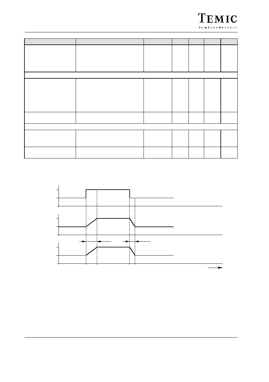
Timing Diagrams
14.0 V
12.0 V
V
Supply
10.7 V
8.7 V
V
SC
10.7 V
8.7 V
V
OUTx
0.4 ms
0.2 ms
t
13841
Figure 5. Variation of power supply
U6268B
Preliminary Information
TELEFUNKEN Semiconductors
Rev. A1, 21-May-97
9 (12)
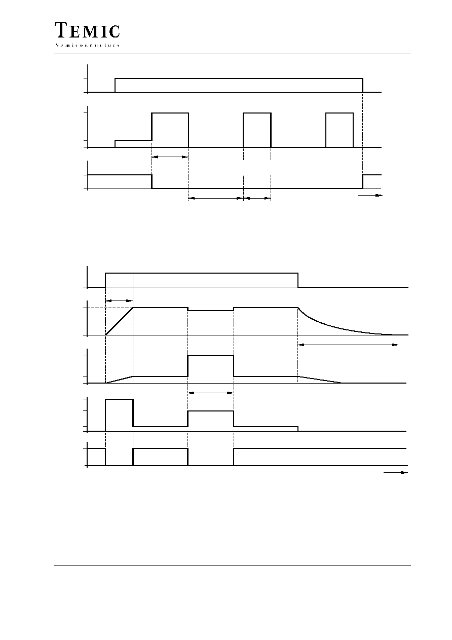
5.0 V
V
ENABLEx
75 mA
15 mA
I
OUTx
overcurrent
overtemperature
shut down
5.0 V
V
CLLx
100 ms
150 ms
75 ms
Pause / pulse for example
(Pulse / pause time depends on power
disipation and R
thja
)
t
13842
overcurrent
overcurrent
Figure 6. Overcurrent protection
30
�
s
200 mV
150
�
s
13 V
discharge of
C
OUT
= 47 nF
with internal current
charge
time
C
OUT
=
47 nF
current
modulation
from
sensor
50
�
s
40 mA
10 mA
V
ENABLEx
V
OUTx
I
OUTx
4.7 V
3.0 V
0.75 V
V
OCMx
5.0 V
0 V
V
CLLx
t
13840
overcurrent
Figure 7. Data transmission

U6268B
TELEFUNKEN Semiconductors
Rev. A1, 21-May-97
Preliminary Information
10 (12)
Application Circuit
5 V
47 nF
47 nF
Out1
Return1
Enable1
OCM1
Enable2
CLL2
OCM2
U6268B
Interface1
Interface2
22 nF
GND
SC
V
CC
= 5V
+V
Batt
I/O
I/O
I/O
Sensor 1
Sensor 2
96 11710
V
S
mC
220
mF
100 nF
CLL1
I/O
1, 8,
9, 16
6
14
15
13
11
10
12
4
3
2
5 V
47 nF
47 nF
Out2
Return2
5
7
V
CC
= 5V
750
750
U6268B
Preliminary Information
TELEFUNKEN Semiconductors
Rev. A1, 21-May-97
11 (12)
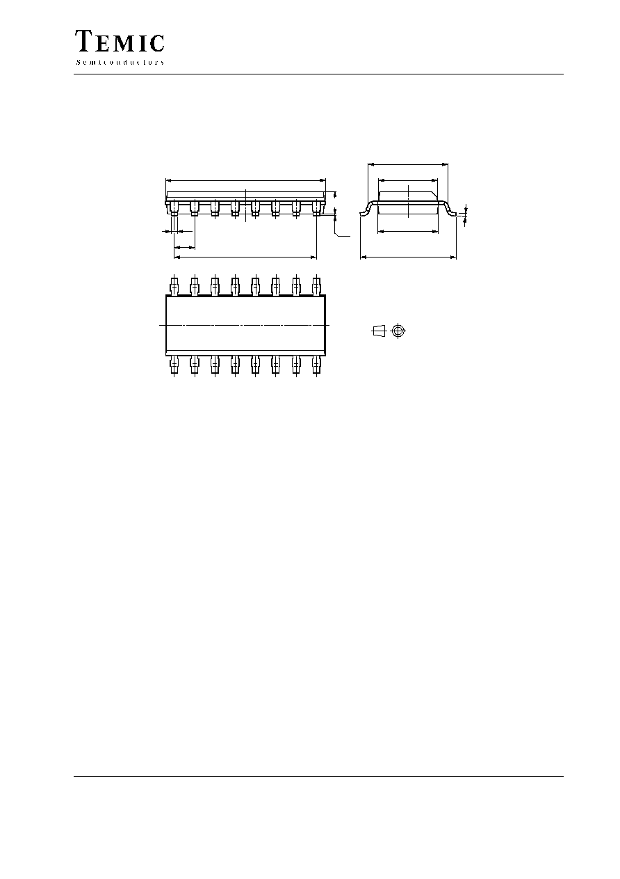
Package Information
13036
technical drawings
according to DIN
specifications
Package SO16
Dimensions in mm
10.0
9.85
8.89
0.4
1.27
1.4
0.25
0.10
5.2
4.8
3.7
3.8
6.15
5.85
0.2
16
9
1
8

U6268B
TELEFUNKEN Semiconductors
Rev. A1, 21-May-97
Preliminary Information
12 (12)
Ozone Depleting Substances Policy Statement
It is the policy of TEMIC TELEFUNKEN microelectronic GmbH to
1. Meet all present and future national and international statutory requirements.
2. Regularly and continuously improve the performance of our products, processes, distribution and operating systems
with respect to their impact on the health and safety of our employees and the public, as well as their impact on
the environment.
It is particular concern to control or eliminate releases of those substances into the atmosphere which are known as
ozone depleting substances ( ODSs ).
The Montreal Protocol ( 1987 ) and its London Amendments ( 1990 ) intend to severely restrict the use of ODSs and
forbid their use within the next ten years. Various national and international initiatives are pressing for an earlier ban
on these substances.
TEMIC TELEFUNKEN microelectronic GmbH semiconductor division has been able to use its policy of
continuous improvements to eliminate the use of ODSs listed in the following documents.
1. Annex A, B and list of transitional substances of the Montreal Protocol and the London Amendments respectively
2 . Class I and II ozone depleting substances in the Clean Air Act Amendments of 1990 by the Environmental
Protection Agency ( EPA ) in the USA
3. Council Decision 88/540/EEC and 91/690/EEC Annex A, B and C ( transitional substances ) respectively.
TEMIC can certify that our semiconductors are not manufactured with ozone depleting substances and do not contain
such substances.
We reserve the right to make changes to improve technical design and may do so without further notice.
Parameters can vary in different applications. All operating parameters must be validated for each customer
application by the customer. Should the buyer use TEMIC products for any unintended or unauthorized
application, the buyer shall indemnify TEMIC against all claims, costs, damages, and expenses, arising out of,
directly or indirectly, any claim of personal damage, injury or death associated with such unintended or
unauthorized use.
TEMIC TELEFUNKEN microelectronic GmbH, P.O.B. 3535, D-74025 Heilbronn, Germany
Telephone: 49 ( 0 ) 7131 67 2831, Fax number: 49 ( 0 ) 7131 67 2423