 | –≠–ª–µ–∫—Ç—Ä–æ–Ω–Ω—ã–π –∫–æ–º–ø–æ–Ω–µ–Ω—Ç: U642B | –°–∫–∞—á–∞—Ç—å:  PDF PDF  ZIP ZIP |
U642B
TELEFUNKEN Semiconductors
Rev. A1, 13-Feb-97
1 (6)
Automotive Wipe/Wash or Interval Switch
Description
As a convenience feature of the windshield wiper inter-
mittent and wipe/wash operation are implemented in
most of the automobiles. The U642B controls all timing
functions accurately at a reasonable price level. Interval
pause and afterwiping time can be set to fixed values with
the help of resistors in a broad time range. Added value
can be provided with an individual, continuous adjust-
ment of the interval pause by a potentiometer which may
be built into the stalk. For proper operation it is mandatory
to feed the signal of the wiper motor`s park switch into
U642B.
Features
D Interval pause: 4 to 20 s
D Afterwiping time: 2 to 20 s
D Wiper motor's park switch
D Wipe/wash mode priority
D One external capacitor, determines all time sequences
D Relay driver with Z-diode
D Interference protection according to VDE 0839 or
ISO/TR 7637/1
D Load-dump protected
Ordering Information
Extended Type Number
Package
Remarks
U642B
DIP8
U642B≠FP
SO8
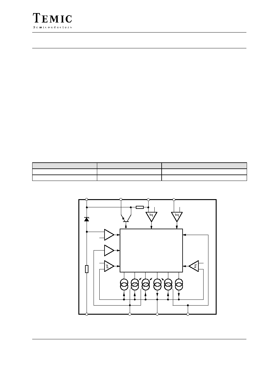
Block Diagram
Wipe / wash
comparator
Interval
comparator
Load-dump
comparator
VRef
VRef
VRef
Input
comparator
Park switch
comparator
VRef
8
7
6
5
4
1
2
3
A
B
C
D
E
F
Logic
VS
Relay control
S1
WI WA
Timing (R)
GND
Interval switch
Timing (C2)
94 8950
Figure 1. Block diagram

U642B
TELEFUNKEN Semiconductors
Rev. A1, 13-Feb-97
2 (6)
Pin Configuration
Pin
Symbol
Function
1
GND
Ground
2
Input 1
Interval switch
3
t
c
Timing capacitor C
2
4
R
4
Afterwiping time resistance
5
WIWA
Wipe/Wash switch
6
S
1
Park switch for wiper motor
7
RELAY
Relay control output
8
+V
Batt
Supply voltage KI. 15
+V
Batt
RELAY
WIWA
GND
Input 1
R
4
t
c
1
2
3
4
8
7
6
5
U642B
93 7691
S
1
Figure 2. Pinning
Circuit Description
Interval Function, Pin 2
By closing the internal switch, S
2
, to supply voltage,
+V
Batt
, the motor is activated. The internal current source
(Pin 3) which holds the capacitor C
2
in charged state is
switched-OFF. As soon as there is a positive potential at
the park switch (S
1
), current source F (see figure 1)
charges the capacitor C
2
very fast. After the wiper
operation is finished, S
1
is again at ground potential, the
relay is in OFF position ≠ interval pause begins ≠ the
capacitor C
2
is discharged through the current source C,
till the voltage at Pin 3 is below the threshold of 2 V.
Interval pause can be adjusted between 4 s to 20 s with the
help of potentiometer R
3
. Now the relay switches ON and
the next interval cycle begins. Opening switch S
2
causes
current source A to discharge C
2
immediately and current
sources C and F are switched-OFF.
Wipe/Wash (WIWA) Operation, Pin 5
By closing the WIWA-switch, S
3
, to supply voltage,
+V
Batt
, water pump starts spraying the water on the wind-
screen, the current source A is switched-OFF which keeps
the capacitor C
2
in discharged state. Now the capacitor is
charged through the current sources D and F, and when af-
ter a time interval of approximately 100 ms, the voltage
at the capacitor is greater than 6.5 V, the relay is turned
on as long as the switch "WIWA" is closed.
The after-wipe-time begins after the switch is open
whereas the sources D and F are switched OFF and the
source E is activated. Source E discharges the capacitor
till the voltage is less than 2.2 V. The relay is OFF and the
wiper-motor is switched OFF. The after-wipe-time is
determined by the current source E which can be
regulated with the external resistor R
Time
. Afterwards the
source A discharges the capacitor. Relay switch OFF is
independent of the park switch S
1
.
Interval and WIWA Functions
The interval function is interrupted immediately when the
switch S
2
is activated. The current source A discharges
the capacitor to a value of 2 V, afterwards the normal S
2
function starts.
Interval wiping starts immediately when the after-wipe-
time is over. The switching delays are slightly shorter,
because the capacitor is already charged to a value of 2 V.
The Wipe/Wash function is not interrupted when interval
switch S
2
is activated. Interval function begins after the
WIWA function is over.

U642B
TELEFUNKEN Semiconductors
Rev. A1, 13-Feb-97
3 (6)
1
2
6
5
8
7
3
4
10 k
W
10 k
W
R
6
R
5
C
1
47
mF
10 V
R
2
C
2
22
mF
10 V
R
4
R
time
= 130 k
W
R
1
510
W
10 k
W
R
3
S
2
S
3
M
M
Relay
Park
switch
31
15
Wiper motor
Interval switch
Water pump
94 8951
S
1
WIWA
U642B
2.7 k
W
Figure 3. Application circuit with interval and wipe/wash operation
Absolute Maximum Ratings
Parameters
Symbol
Value
Unit
Supply voltage
t = 60 s
Terminal 15, Pin 8
V
Batt
28
V
Supply current
t = 2 ms
Pin 8
t = 200 ms
I
8
I
8
1.5
150
A
mA
Relay control output current (DC)
Pin 7
t = 200 ms
I
7
I
7
200
1.2
mA
A
Pulse current (control inputs)
t = 200 ms
Park switch, S
1
Pin 6
Wipe/Wash switch, S
3
Pin 5
Interval switch, S
2
Pin 2
I
6
I
5
I
2
50
50
50
mA
Power dissipation
T
amb
= 90
∞
C
P
tot
500
mW
Storage temperature range
T
stg
≠55 to +125
∞
C
Ambient temperature range
T
amb
≠40 to +85
∞
C

U642B
TELEFUNKEN Semiconductors
Rev. A1, 13-Feb-97
4 (6)
Thermal Resistance
Parameters
Symbol
Value
Unit
Junction ambient
DIP8
SO8
R
thJA
R
thJA
110
160
K/W
K/W
Electrical Characteristics
V
Batt
= 12 V, T
amb
= 25
∞
C, (see figure KEIN MERKER) unless otherwise specified.
Parameters
Test Conditions / Pins
Symbol
Min.
Typ.
Max.
Unit
Supply voltage
Pin 8
V
Batt
9
16.5
V
Supply current
I
8
10
mA
Z-diode limitation
V
2
≠7.6
V
Overvoltage
Threshold current
I1
≠50
mA
Threshold voltage
V
Batt
35
V
Relay control output
Pin 7
Saturation voltage
I
7
= 100 mA
I
7
= 200 mA
V
7
≠1.0
≠1.5
V
Reverse current
I
7
≠0.1
mA
Park switch
Pin 6
Internal pull-up resistance
R
6
= 10 k
W
R
6
50
k
W
Switching threshold voltage
V
6
≠3.3
V
Protection diode
I
6
= ≠10 mA
I
6
= 10 mA
V
6
V
6
≠0.8
7.6
V
V
Input C
2
Pin 3
Internal resistance
R
3
100
W
Interval input, R
2
= 2.7 to 30 k
W
Pin 2
Protection diode
I
2
= ≠10 mA
I
2
= 30 mA/10 ms
V
2
≠0.8
7.6
V
WIWA Input, R
5
= 10 k
W
Pin 5
Switching threshold/
Hysteresis
V
5
≠1.4/≠5.4
V
Protection diode
I
5
= ≠10 mA
I
5
= 10 mA
V
≠0.8
7.6
V
Switching Characteristics, R
4
= 47 k
W to 300 kW, I
4
= ≠150
mA
Interval time
R
3
= 0 k
W
R
3
= 10 k
W
t
2
3.6
10.8
4
12
4.4
13.2
s
Switch-ON time
t
on
100
ms
After-wipe-time
R
4
= 130 k
W Pin 5
t
5
4.75
5.25
5.75
s
U642B
TELEFUNKEN Semiconductors
Rev. A1, 13-Feb-97
5 (6)
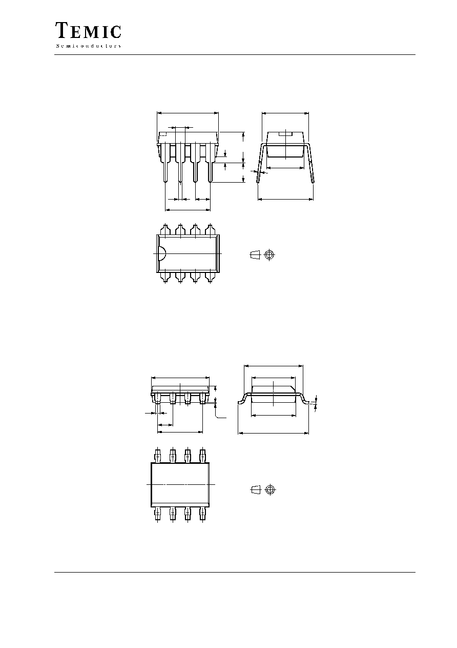
Package Information
13021
9.8
9.5
Package DIP8
Dimensions in mm
1.64
1.44
4.8 max
0.5 min
3.3
0.58
0.48
7.62
2.54
6.4 max
0.36 max
9.8
8.2
7.77
7.47
8
5
1
4
technical drawings
according to DIN
specifications
13034
technical drawings
according to DIN
specifications
Package SO8
Dimensions in mm
5.00
4.85
0.4
1.27
3.81
1.4
0.25
0.10
5.2
4.8
3.7
3.8
6.15
5.85
0.2
8
5
8
5

U642B
TELEFUNKEN Semiconductors
Rev. A1, 13-Feb-97
6 (6)
Ozone Depleting Substances Policy Statement
It is the policy of TEMIC TELEFUNKEN microelectronic GmbH to
1. Meet all present and future national and international statutory requirements.
2. Regularly and continuously improve the performance of our products, processes, distribution and operating systems
with respect to their impact on the health and safety of our employees and the public, as well as their impact on
the environment.
It is particular concern to control or eliminate releases of those substances into the atmosphere which are known as
ozone depleting substances ( ODSs ).
The Montreal Protocol ( 1987 ) and its London Amendments ( 1990 ) intend to severely restrict the use of ODSs and
forbid their use within the next ten years. Various national and international initiatives are pressing for an earlier ban
on these substances.
TEMIC TELEFUNKEN microelectronic GmbH semiconductor division has been able to use its policy of
continuous improvements to eliminate the use of ODSs listed in the following documents.
1. Annex A, B and list of transitional substances of the Montreal Protocol and the London Amendments respectively
2 . Class I and II ozone depleting substances in the Clean Air Act Amendments of 1990 by the Environmental
Protection Agency ( EPA ) in the USA
3. Council Decision 88/540/EEC and 91/690/EEC Annex A, B and C ( transitional substances ) respectively.
TEMIC can certify that our semiconductors are not manufactured with ozone depleting substances and do not contain
such substances.
We reserve the right to make changes to improve technical design and may do so without further notice.
Parameters can vary in different applications. All operating parameters must be validated for each customer
application by the customer. Should the buyer use TEMIC products for any unintended or unauthorized
application, the buyer shall indemnify TEMIC against all claims, costs, damages, and expenses, arising out of,
directly or indirectly, any claim of personal damage, injury or death associated with such unintended or
unauthorized use.
TEMIC TELEFUNKEN microelectronic GmbH, P.O.B. 3535, D-74025 Heilbronn, Germany
Telephone: 49 ( 0 ) 7131 67 2831, Fax number: 49 ( 0 ) 7131 67 2423