U6433B
TELEFUNKEN Semiconductors
Rev. A3, 25-Feb-97
1 (5)
Flasher, 18-m
W Shunt, Frequency Doubling Disabling
Description
The design of the U6433B is mainly based on the good
results of U6043B in terms of EMC (Electro Magnetic
Capability) and protection features. It includes an
additional 8-mV comparator and a logical connection
with the frequency doubling stage. This combination can
be used for a hazard switch which bypasses the external
shunt resistor to disable the frequency doubling. This fea-
ture can be useful in the US automotive industry. During
direction mode the U6433B works like other flashers, i.e.,
frequency doubling in the case of lamp outage.
Features
D Temperature and voltage compensated frequency
D Warning indication of lamp failure by means of
frequency doubling can be disabled
D Voltage dependence of the car indicator lamps
compensated for lamp failure
D Relay output with high current carrying capacity
and low saturation voltage
D Minimum lamp load for flasher operationy 1 W
D Load-dump protection
D Very low susceptibility to EMI
D Protection according to ISO/TR 7637/1 level 4
Ordering Information
Extended Type Number
Package
Remarks
U6433B�FP
SO8
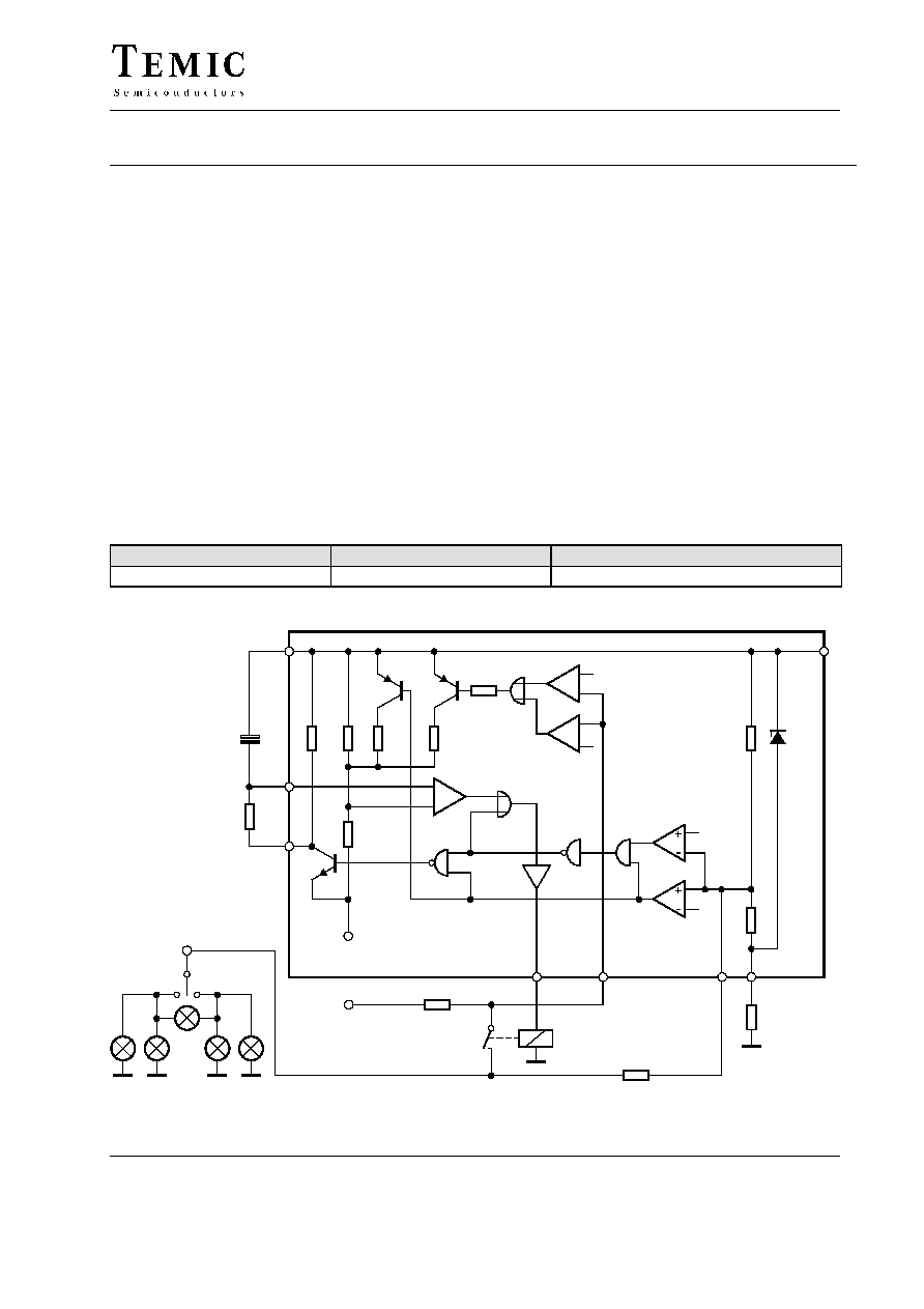
Block Diagram
V
S
� 49 mV
V
S
� 8 mV
G
4
G
2
+
�
+
�
+
�
G
5
D
1
2
V
S
8
1
7
3
23 V
470
W
R
4
V
S
�6 V
6
4
5
4.7
mF
R
1
82 k
W
94 9289
V
S
� 4 V
V
S
� 8 V
C
1
V
S
49 a
Shunt
R
3
18 m
W
R
2
1.5 k
W
P
L
>1 W
K
1
K
4
K
5
K
2
K
3
Figure 1. Application circuit as a car flasher
U6433B
TELEFUNKEN Semiconductors
Rev. A3, 25-Feb-97
2 (5)
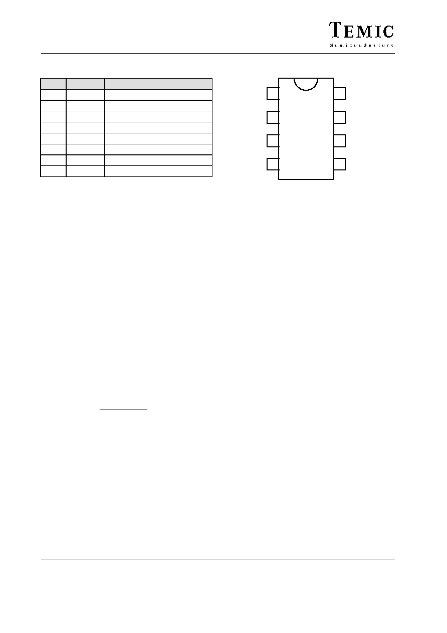
Pin Description
Pin
Symbol
Function
1
GND
IC ground
2
V
S
Supply voltage
3
REL
Relay driver
4
OSC
Oscillator
5
OSC
Oscillator
6
V
S
Supply voltage
7
LD
Lamp failure detection
8
SI
Start input (49a)
1
2
3
4
8
7
6
5
GND
REL
OSC
SI
LD
Vs
OSC
U6433B
V
S
13298
Figure 2. Pinning
Functional Description
Pin 1, GND
The integrated circuit is protected against damage via
resistor R
4
to ground (�31) in the case of battery reversal.
An integrated protection circuit together with external
resistances R
2
and R
4
limits the current pulses in the IC.
Pin 2, Supply voltage, V
S
- Power
The arrangement of the supply connections to Pin 2 must
be such as ensure that, on the connection printed circuit
board (PCB), the resistance of V
S
to Pin 6 is lower than
that to Pin 2.
Pin 3, Relay control output (driver)
The relay control output is a high-side driver with a low
saturation voltage and capable to drive a typical
automotive relay with a minimum coil resistance of 60
W.
Pin 4 and 5 Oscillator
Flashing frequency, f
1
, is determined by the R
1
C
1
components as follows (see figure 1):
f
1
[
1
R
1
C
1
1.5
Hz
where
C
1
47
mF
R
1
+ 6.8 kW to 510 kW
In the case of a lamp outage (see Pin 7) the oscillator
frequency is switched to the lamp outage frequency f
2
with f
2
[ 2.2 f
1
.
Duty cycle in normal flashing mode: 50%
Duty cycle in lamp outage mode: 40% (bright phase)
Pin 6, Supply voltage, Sense
For accurate monitoring via the shunt resistor, a mini-
mized layer resistance from point V
S
/ shunt to Pin 6 is
recommended.
Pin 7, Lamp outage detection
Control Signal Threshold 1 ( 49-mV Comparator K1)
The detection point for lamp failure can be calculated
from the control signal threshold, typically 49 mV with
V
S
= 12 V. With a measuring resistance of R
3
= 18 m
W,
the frequency changeover is reached at a lamp load of
21
W
+
11.4
W. The variation of the control signal
threshold supply voltage takes into account the PTC char-
acteristic of filament lamps.
Control Signal Threshold 2 ( 8-mV Comparator K4)
A voltage drop at R
3
between 49 mV and 8 mV shunt
resistor let the flasher work in frequency doubling mode.
If the voltage drop of V
R3MAX
= 8 mV falls the frequency
doubling is disabled. This can be achieved either with a
switch which by passes the shunt resistor ( e.g., a special
hazard warning switch ) or with a small lamp load.
The arrangement of the supply connections to Pins 2 and
6 must ensure that, on the connection, PCB, the layer
resistance from V
S
to Pin 6 is lower than the one to Pin 2.
Flasher operation starts with a lamp load of P
L
y 1 W.
Pin 8, Start input
Start condition for flashing: the voltage at Pin 8 has to be
below K3 threshold (flasher switch closed).
Humidity and dirt may decrease the resistance between
49 a and GND. If this leakage resistance is
u 5 kW the IC
is still kept in its off-condition. In this case the voltage at
Pin 8 is between the thresholds of comparators K2 and
K3.
During the bright phase the voltage at Pin 8 is above the
K2
threshold, during the dark phase it is below the K3
threshold.
For proper start conditions a minimum lamp wattage of
1 W is required.

U6433B
TELEFUNKEN Semiconductors
Rev. A3, 25-Feb-97
3 (5)
Absolute Maximum Ratings
Reference point Pin 1
Parameters
Symbol
Value
Unit
Supply voltage
Pins 2 and 6
V
S
18
V
Surge forward current
t
p
= 0.1 ms
Pins 2 and 6
t
p
= 300 ms
Pins 2 and 6
t
p
= 300 ms
Pin 8
I
FSM
1.5
1.0
30.0
A
A
mA
Output current
Pin 3
I
O
0.3
A
Power dissipation
T
amb
= 95
_C
SO 8
T
amb
= 60
_C
SO 8
P
tot
340
560
mW
mW
Junction temperature
T
j
150
_C
Ambient temperature range
T
amb
� 40 to + 105
_C
Storage temperature range
T
stg
� 55 to + 150
_C
Thermal Resistance
Parameters
Symbol
Value
Unit
Junction ambient
SO8
R
thJA
160
K/W
Electrical Characteristics
Typical values under normal operation of the application circuit shown in figure 1, V
S
= 12 V (Pins 2 and 6).
T
amb
= 25
_C, reference point ground (�31), unless otherwise specified.
Parameters
Test conditions / Pin
Symbol
Min.
Typ.
Max.
Unit
Supply voltage range
Pins 2 and 6
V
S
9
16.5
V
Supply current, dark phase
Pins 2 and 6
I
S
4.5
8
mA
Supply current, bright
phase
Pins 2 and 6
I
S
7.0
11
mA
Relay output, saturation
voltage
I
O
= 150 mA,
V
S
= 9 V
Pin 3
V
O
1.0
V
Relay output reverse
current
Pin 3
I
O
0.1
mA
Relay coil resistance
R
L
60
W
Start delay
First bright phase
t
on
10
ms
Frequency determining
resistor
R
1
6.8
510
k
W
Frequency determining
capacitor
C
1
47
mF
Frequency tolerance
Normal flashing, basic
frequency f
1
not including
the tolerances of the exter-
nal components R
1
and C
1
f
1
� 5
+ 5
%
Bright period
Basic frequency f
1,
V
S
= 9 � 15 V
f
1
47
53
%
Bright period
Control frequency f
2,
V
S
= 9 � 15 V
f
2
37
45
%
Frequency increase
Lamp failure,
V
S
= 9 � 15 V
f
2
2.15
f
1
2.3
f
1
Hz

U6433B
TELEFUNKEN Semiconductors
Rev. A3, 25-Feb-97
4 (5)
Electrical Characteristics (continued)
Parameters
Test conditions / Pin
Symbol
Min.
Typ.
Max.
Unit
Control signal threshold 1
V
S
= 15 V
Pin 7
V
S
= 9 V
V
S
= 12 V
V
R3
50
43
47
53
45
49
57
47
51
mV
Control signal threshold 2
V
R3
2
10
mV
Leakage resistance
49a to GND
R
p
5
k
W
Lamp load
P
L
1
W
Package Information
13034
technical drawings
according to DIN
specifications
Package SO8
Dimensions in mm
5.00
4.85
0.4
1.27
3.81
1.4
0.25
0.10
5.2
4.8
3.7
3.8
6.15
5.85
0.2
8
5
8
5

U6433B
TELEFUNKEN Semiconductors
Rev. A3, 25-Feb-97
5 (5)
Ozone Depleting Substances Policy Statement
It is the policy of TEMIC TELEFUNKEN microelectronic GmbH to
1. Meet all present and future national and international statutory requirements.
2. Regularly and continuously improve the performance of our products, processes, distribution and operating systems
with respect to their impact on the health and safety of our employees and the public, as well as their impact on
the environment.
It is particular concern to control or eliminate releases of those substances into the atmosphere which are known as
ozone depleting substances ( ODSs ).
The Montreal Protocol ( 1987 ) and its London Amendments ( 1990 ) intend to severely restrict the use of ODSs and
forbid their use within the next ten years. Various national and international initiatives are pressing for an earlier ban
on these substances.
TEMIC TELEFUNKEN microelectronic GmbH semiconductor division has been able to use its policy of
continuous improvements to eliminate the use of ODSs listed in the following documents.
1. Annex A, B and list of transitional substances of the Montreal Protocol and the London Amendments respectively
2 . Class I and II ozone depleting substances in the Clean Air Act Amendments of 1990 by the Environmental
Protection Agency ( EPA ) in the USA
3. Council Decision 88/540/EEC and 91/690/EEC Annex A, B and C ( transitional substances ) respectively.
TEMIC can certify that our semiconductors are not manufactured with ozone depleting substances and do not contain
such substances.
We reserve the right to make changes to improve technical design and may do so without further notice.
Parameters can vary in different applications. All operating parameters must be validated for each customer
application by the customer. Should the buyer use TEMIC products for any unintended or unauthorized
application, the buyer shall indemnify TEMIC against all claims, costs, damages, and expenses, arising out of,
directly or indirectly, any claim of personal damage, injury or death associated with such unintended or
unauthorized use.
TEMIC TELEFUNKEN microelectronic GmbH, P.O.B. 3535, D-74025 Heilbronn, Germany
Telephone: 49 ( 0 ) 7131 67 2831, Fax number: 49 ( 0 ) 7131 67 2423