
U7001BG
Preliminary Information
TELEFUNKEN Semiconductors
Rev. A3, 05-Jul-96
1 (11)
CT2 Front End IC
Description
U7001BG is a monolithic GaAs transmit/ receive front
end with power amplifier, low noise amplifier and
antenna switch. It is specially designed for operation in
CT2 band and suitable for a frequency range of 839 MHz
to 952 MHz with external matching.
Electrostatic sensitive device.
Observe precautions for handling.
Features
D Low supply voltage 3.6 V typical (min. 2.7 V)
D High power added efficiency (typ. 40%)
D Low power consumption in receive mode
D Power down control pin for low noise amplifier
D Gain control of power amplifier
D Low noise amplifier
D Optional high output power 50 mW @ 5 V supply
voltage
D SSO20 plastic package
Benefits
D Extended talk time due to low power consumption and
high PAE
D Few external components and very small package
save space
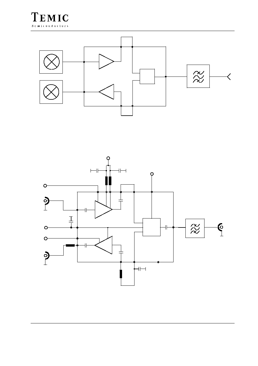
Block Diagram
PA
LNA
Switch
PA In
LNA Ctrl
LNA Out
VDD(PA)
PA Ctrl
PA Out
SW TX
LNA In
SW RX
GND
SW Ant
8
3
6
7
4
1
5,9,10,11,13,15,19
20
18
17
16
LNA /SW VDD
12
14
SW Ctrl
2
94 8824
Figure 1. Block diagram

U7001BG
TELEFUNKEN Semiconductors
Rev. A3, 05-Jul-96
Preliminary Information
2 (11)
Pin Description
1
2
3
4
5
6
7
8
9
10
11
12
13
14
15
16
17
18
19
20
U7001BG
SW RX
SW Ctrl
LNA Ctrl
LNA In
LNA/SW VDD
LNA Out
GND
PA In
SW Ant
GND
SW TX
PA Out
PA VDD2
GND
GND
GND
PA Ctrl
GND
GND
PA VDD1
94 8825
Pin
Symbol
Function
���
���
1
�����
�����
SW RX
����������
����������
Switch RX output
���
���
2
�����
�����
SW Ctrl
����������
����������
Switch control input
���
���
3
�����
�����
LNA Ctrl
����������
����������
LNA control input
���
���
4
�����
�����
LNA In
����������
����������
Low noise amplifier input
���
�
�
�
���
5,9,10,
11,13
15,19
�����
�
���
�
�����
GND
����������
���������
�
����������
Ground
���
���
6
�����
�����
LNA Out
����������
����������
LNA output
���
�
�
�
���
7
�����
�
���
�
�����
LNA/SW
VDD
����������
���������
�
����������
LNA & Switch power supply
voltage
���
���
8
�����
�����
PA In
����������
����������
Power amplifier input
���
���
12
�����
�����
PA Ctrl
����������
����������
PA control input
���
���
14
�����
�����
PA VDD1
����������
����������
PA power supply voltage 1
���
���
16
�����
�����
PA VDD2
����������
����������
PA power supply voltage 2
���
���
17
�����
�����
PA Out
����������
����������
PA output
���
���
18
�����
�����
SW TX
����������
����������
Switch TX input
���
���
20
�����
�����
SW Ant
����������
����������
Switch antenna output
Absolute Maximum Ratings
Parameters
Symbol
Value
Unit
�����������������
�����������������
Supply voltages
Pins 7, 14 and 16
�����
�����
VDD
��������
��������
+ 7
�����
�����
V
�����������������
�����������������
Input voltages
Pins 4, 8, 18 and 20
�����
�����
V
i
��������
��������
0 to VDD
�����
�����
V
�����������������
�����������������
Control voltages
Pins 2, 3 and 12
�����
�����
V
C
��������
��������
0 to VDD
�����
�����
V
�����������������
�����������������
Channel temperature
�����
�����
T
ch
��������
��������
125
�����
�����
�
C
�����������������
�����������������
Storage temperature range
�����
�����
T
stg
��������
��������
� 40 to + 125
�����
�����
�
C
Thermal Resistance
Parameters
Symbol
Value
Unit
�����������������
�����������������
Channel ambient
SSO20
�����
�����
R
thch
��������
��������
140
�����
�����
K/W
Operating Range
Parameters
Symbol
Value
Unit
�����������������
�
���������������
�
�����������������
Supply voltage
Pin 7
�����
�
���
�
�����
LNA/SW
VDD
��������
�
������
�
��������
2.7 to 5.25
�����
�
���
�
�����
V
�����������������
�����������������
Supply voltage
Pins 14 and 16
�����
�����
VDD
��������
��������
2.7 to 5.25
�����
�����
V
�����������������
�����������������
Ambient temperature range
�����
�����
T
amb
��������
��������
� 40 to + 85
�����
�����
�
C
U7001BG
Preliminary Information
TELEFUNKEN Semiconductors
Rev. A3, 05-Jul-96
3 (11)
Electrical Characteristics Low Noise Amplifier (LNA)
Test conditions (unless otherwise specified): VDD = 3.3 V, T
amb
= 25
�
C, referred to test circuit.
System impedance Zo = 50
W, f
RF
= 866 MHz
Parameters
Test Conditions / Pins
Symbol
Min.
Typ.
Max.
Unit
���������
���������
Supply voltage range
��������
��������
Pin 7
����
����
VDD
�����
�����
2.9
����
����
3.6
����
����
5.25
����
����
V
���������
���������
Supply current
��������
��������
@ VDD = 2.9 V, Pin 7
����
����
Is
�����
�����
����
����
3.5
����
����
5.0
����
����
mA
Supply current
@ VDD = 2.9 V, Pin 7;
LNA Ctrl = 0 V:
LNA"off"
Is
0.5
mA
���������
���������
Frequency range
��������
��������
Pin 4
����
����
f
�����
�����
839
����
����
866
����
����
952
����
����
MHz
���������
���������
Linear power gain
��������
��������
Pins 4 and 6
����
����
Gp
�����
�����
����
����
14
����
����
����
����
dB
���������
���������
Noise figure
��������
��������
Pins 4 and 6
����
����
NF
�����
�����
����
����
2.0
����
����
2.5
����
����
dB
���������
���������
Compression
��������
��������
Pins 4 and 6
����
����
P_1dB
�����
�����
� 29
����
����
� 27
����
����
����
����
dBm
���������
�
�������
�
���������
Third order input intercept
point
��������
�
������
�
��������
Pins 4 and 6
����
�
��
�
����
IIP3
�����
�
���
�
�����
� 19
����
���
�
����
� 17
����
�
��
�
����
����
�
��
�
����
dBm
���������
���������
Isolation
��������
��������
Pins 6 and 4
(from output to input)
����
����
Isol
LNA
�����
�����
20
����
����
25
����
����
����
����
dB
���������
���������
Input impedance
��������
��������
Pin 4
����
����
�����
�����
����
����
50
����
����
����
����
W
���������
���������
Output impedance
��������
��������
Pin 6
����
����
�����
�����
50
����
����
100
����
����
����
����
W
LNA control voltage
Pin 3: LNA Mode "off"
Pin 3: LNA Mode "on"
LNA Ctrl
VDD�0.5
0.0
VDD
0.5
V
Test conditions (unless otherwise specified); VDD = 2.9 V, T
amb
= 25
�
C, referred to test circuit.
System impedance Zo = 50
W; f
RF
= 866 MHz
Parameters
Test Conditions / Pins
Symbol
Min.
Typ.
Max.
Unit
���������
���������
Supply voltage range
��������
��������
Pin 7
����
����
VDD
�����
�����
2.9
����
����
3.6
����
����
5.25
����
����
V
���������
���������
Supply current
��������
��������
@ VDD = 2.7 V, Pin 7
����
����
Is
�����
�����
����
����
3.0
����
����
4.0
����
����
mA
Supply current
@ VDD = 2.7 V, Pin 7;
LNA Ctrl = 0 V:
LNA"off"
Is
0.5
mA
���������
���������
Frequency range
��������
��������
Pin 4
����
����
f
�����
�����
839
����
����
866
����
����
952
����
����
MHz
���������
���������
Linear power gain
��������
��������
Pins 4 and 6
����
����
Gp
�����
�����
����
����
12
����
����
����
����
dB
���������
���������
Noise figure
��������
��������
Pins 4 and 6
����
����
NF
�����
�����
����
����
2.0
����
����
2.5
����
����
dB
���������
���������
Compression
��������
��������
Pins 4 and 6
����
����
P_1dB
�����
�����
� 29
����
����
� 28
����
����
����
����
dBm
���������
�
�������
�
Third order input intercept
point
��������
�
������
�
Pins 4 and 6
����
�
��
�
IIP3
�����
�
���
�
� 19
����
���
�
� 18
����
�
��
�
����
�
��
�
dBm
���������
�
�������
�
���������
Isolation
��������
�
������
�
��������
Pins 6 and 4
(from output to input)
����
�
��
�
����
Isol
LNA
�����
�
���
�
�����
20
����
���
�
����
25
����
�
��
�
����
����
�
��
�
����
dB
���������
���������
Input impedance
��������
��������
Pin 4
����
����
�����
�����
����
����
50
����
����
����
����
W
���������
���������
Output impedance
��������
��������
Pin 6
����
����
�����
�����
50
����
����
100
����
����
����
����
W
LNA control voltage
Pin 3: LNA Mode "off"
Pin 3: LNA Mode "on"
LNA
Ctrl
VDD�0.5
0.0
VDD
0.5
V

U7001BG
TELEFUNKEN Semiconductors
Rev. A3, 05-Jul-96
Preliminary Information
4 (11)
Electrical Characteristics Power Amplifier
Test conditions (unless otherwise specified); VDD = 5.0 V, PA Ctrl = 5 V, Tamb = 25
�
C, referred to test circuit.
System Impedance Zo = 50
W; f
RF
= 866 MHz
Parameters
Test Conditions / Pins
Symbol
Min.
Typ.
Max.
Unit
���������
���������
Supply voltage range
��������
��������
Pins 14 and 16
����
����
VDD1,2
�����
�����
2.7
����
����
3.6
����
����
5.25
����
����
V
���������
���������
Supply current
��������
��������
Pins 14 and 16
����
����
Is
�����
�����
����
����
33
����
����
40
����
����
mA
Supply current
Pin 12
I Ctrl
5.0
6.0
mA
���������
���������
Frequency range
��������
��������
Pin 8
����
����
f
�����
�����
839
����
����
866
����
����
952
����
����
MHz
���������
���������
Linear power gain
��������
��������
Pins 8 and 17
����
����
Gp
�����
�����
34
����
����
36
����
����
����
����
dB
���������
Power response
��������
@ P
in
= � 14 dBm
����
�����
����
����
����
���������
�
�������
�
���������
Output Power
��������
�
������
�
��������
At 3 dB gain compression;
Pin 17
����
�
���
����
P
out
�����
�
���
�
�����
17
����
�
��
�
����
18
����
�
��
�
����
����
�
��
�
����
dBm
���������
���������
Gain control range
��������
��������
Pins 17 and 12
����
����
G
c
�����
�����
30
����
����
33
����
����
����
����
dB
���������
���������
Gain control voltage
��������
��������
Pout = Pout
max
����
����
PA Ctrl
�����
�����
����
����
4.5
����
����
VDD
����
����
V
���������
���������
Gain control voltage
��������
��������
Pout = Pout
max � 16 dB
����
����
PA Ctrl
�����
�����
����
����
1.2
����
����
����
����
V
Gain control voltage
Pout = Pout
min
PA Ctrl
0.0
V
Switching time
Pins 12 and 17
Turn on time
90% Pout
max
t
on
2
ms
Turn off time
10% Pout
max
t
off
5
ms
���������
���������
Harmonic levels
��������
��������
At 3 dB gain compression
����
����
�����
�����
� 18
����
����
� 25
����
����
����
����
dBc
���������
�
�������
�
���������
Isolation
��������
�
������
�
��������
Pins 17 and 8
(from output to input)
����
�
���
����
Isol
PA
�����
�
���
�
�����
20
����
�
��
�
����
25
����
�
��
�
����
����
�
��
�
����
dB
���������
���������
Input matching
��������
��������
Pin 8
����
����
VSWR
in
�����
�����
1.9 : 1
����
����
1.6 : 1
����
����
����
����
���������
���������
Output matching
��������
��������
Pin 17
����
����
VSWR
out
�����
�����
����
����
2.0 : 1
����
����
����
����
���������
���������
Power added efficiency
��������
��������
Pin 17
����
����
h
PAE
�����
�����
����
����
40
����
����
����
����
%
���������
���������
Input impedance
��������
��������
Pin 8
����
����
Z
in
�����
�����
����
����
50
����
����
����
����
W
���������
���������
Output impedance
��������
��������
Pin 17
����
����
Z
out
�����
�����
����
����
50
����
����
����
����
W
U7001BG
Preliminary Information
TELEFUNKEN Semiconductors
Rev. A3, 05-Jul-96
5 (11)
Electrical Characteristics Power Amplifier
Test conditions (unless otherwise specified); VDD = 3.6 V, PA Ctrl = 3.6 V, Tamb = 25
�
C, referred to test circuit.
System impedance Zo = 50
W; f
RF
= 866 MHz
Parameters
Test Conditions / Pins
Symbol
Min.
Typ.
Max.
Unit
���������
���������
Supply voltage range
��������
��������
Pins 14 and 16
�����
�����
VDD1,2
����
����
2.7
����
����
3.6
����
����
5.25
����
����
V
���������
���������
Supply current
��������
��������
Pins 14 and 16
�����
�����
Is
����
����
����
����
30
����
����
36
����
����
mA
Supply current
Pin 12
I
Ctrl
5.0
6.0
mA
���������
���������
Frequency range
��������
��������
Pin 8
�����
�����
f
����
����
839
����
����
866
����
����
952
����
����
MHz
���������
���������
Linear power gain
��������
��������
Pins 8 and 17
�����
�����
Gp
����
����
32
����
����
35
����
����
����
����
dB
���������
Power response
��������
@ P
in
= � 14 dBm
�����
����
����
����
����
���������
�
�������
�
���������
Output Power
��������
�
������
�
��������
At 3 dB gain compression;
Pin 17
�����
�
���
�
�����
P
out
����
�
��
�
����
15
����
�
��
�
����
17
����
�
��
�
����
����
�
��
�
����
dBm
���������
���������
Gain control range
��������
��������
Pins 17 and 12
�����
�����
G
c
����
����
30
����
����
33
����
����
����
����
dB
���������
���������
Gain control voltage
��������
��������
Pout = Pout
max
�����
�����
PA Ctrl
����
����
����
����
2.9
����
����
VDD
����
����
V
���������
���������
Gain control voltage
��������
��������
Pout = Pout
max � 16 dB
�����
�����
PA Ctrl
����
����
����
����
1.2
����
����
����
����
V
Gain control voltage
Pout = Pout
min
PA Ctrl
0.0
V
Switching time
Pins 12 and 17
Turn on time
90% Pout
max
t
on
2
ms
Turn off time
10% Pout
max
t
off
5
ms
���������
���������
Harmonic levels
��������
��������
At 3 dB gain compression
�����
�����
����
����
� 18
����
����
� 25
����
����
����
����
dBc
���������
�
�������
�
���������
Isolation
��������
�
������
�
��������
Pins 17 and 8
(from output to input)
�����
�
���
�
�����
Isol
PA
����
�
��
�
����
20
����
�
��
�
����
25
����
�
��
�
����
����
�
��
�
����
dB
���������
���������
Input matching
��������
��������
Pin 8
�����
�����
VSWR
in
����
����
1.9 : 1
����
����
1.6 : 1
����
����
����
����
���������
���������
Output matching
��������
��������
Pin 17
�����
�����
VSWR
out
����
����
����
����
2.0 : 1
����
����
����
����
���������
���������
Power added efficiency
��������
��������
Pin 17
�����
�����
h
PAE
����
����
����
����
45
����
����
����
����
%
���������
���������
Input impedance
��������
��������
Pin 8
�����
�����
Z
in
����
����
����
����
50
����
����
����
����
W
���������
���������
Output impedance
��������
��������
Pin 17
�����
�����
Z
out
����
����
����
����
50
����
����
����
����
W

U7001BG
TELEFUNKEN Semiconductors
Rev. A3, 05-Jul-96
Preliminary Information
6 (11)
Electrical Characteristics Power Amplifier
Test conditions (unless otherwise specified); VDD = 2.7 V, PA Ctrl = 2.7 V, T
amb
= 25
�
C, referred to test circuit.
System impedance Zo = 50
W; f
RF
= 866 MHz
Parameters
Test Conditions / Pins
Symbol
Min.
Typ.
Max.
Unit
���������
���������
Supply voltage range
��������
��������
Pins 14 and 16
����
����
VDD1,2
�����
�����
2.7
����
����
3.6
����
����
5.25
����
����
V
���������
���������
Supply current
��������
��������
Pins 14 and 16
����
����
Is
�����
�����
����
����
25
����
����
30
����
����
mA
Supply current
Pin 12
I Ctrl
4.5
5.5
mA
���������
���������
Frequency range
��������
��������
Pin 8
����
����
f
�����
�����
839
����
����
866
����
����
952
����
����
MHz
���������
���������
Linear power gain
��������
��������
Pins 8 and 17
����
����
Gp
�����
�����
30
����
����
32
����
����
����
����
dB
���������
Power response
��������
@ P
in
= �15 dBm
����
�����
����
����
����
���������
�
�������
�
���������
Output Power
��������
�
������
�
��������
At 3 dB gain compression;
Pin 17
����
�
���
����
P
out
�����
�
���
�
�����
12
����
�
��
�
����
14
����
�
��
�
����
����
�
��
�
����
dBm
���������
���������
Gain control range
��������
��������
Pins 17 and 12
����
����
G
c
�����
�����
30
����
����
33
����
����
����
����
dB
���������
���������
Gain control voltage
��������
��������
Pout = Pout
max
����
����
PA Ctrl
�����
�����
����
����
2.7
����
����
VDD
����
����
V
���������
���������
Gain control voltage
��������
��������
Pout = Pout
max � 16 dB
����
����
PA
Ctrl
�����
�����
����
����
1.5
����
����
����
����
V
Gain control voltage
Pout = Pout
min
PA Ctrl
0.0
V
Switching time
Pins 12 and 17
Turn on time
90% Pout
max
t
on
2
ms
Turn off time
10% Pout
max
t
off
5
ms
���������
���������
Harmonic levels
��������
��������
At 3 dB gain compression
����
����
�����
�����
� 20
����
����
� 25
����
����
����
����
dBc
���������
�
�������
�
���������
Isolation
��������
�
������
�
��������
Pins 16, 8
(from output to input)
����
�
���
����
Isol
PA
�����
�
���
�
�����
20
����
�
��
�
����
25
����
�
��
�
����
����
�
��
�
����
dB
���������
���������
Input matching
��������
��������
Pin 8
����
����
VSWR
in
�����
�����
1.9 : 1
����
����
1.4 : 1
����
����
����
����
���������
���������
Output matching
��������
��������
Pin 16
����
����
VSWRout
�����
�����
����
����
2.0 : 1
����
����
����
����
���������
���������
Power added efficiency
��������
��������
Pin 16
����
����
h
PAE
�����
�����
����
����
35
����
����
����
����
%
���������
���������
Input impedance
��������
��������
Pin 8
����
����
Z
in
�����
�����
����
����
50
����
����
����
����
W
���������
���������
Output impedance
��������
��������
Pin 16
����
����
Z
out
�����
�����
����
����
50
����
����
����
����
W

U7001BG
Preliminary Information
TELEFUNKEN Semiconductors
Rev. A3, 05-Jul-96
7 (11)
Electrical Characteristics Antenna Switch
Test conditions (unless otherwise specified); VDD = 3.6 V, Tamb = 25
�
C, referred to test circuit.
System impedance Zo = 50
W; f
RF
= 866 MHz
Parameters
Test Conditions / Pins
Symbol
Min.
Typ.
Max.
Unit
���������
�
�������
�
���������
Supply voltage range
��������
�
������
�
��������
Pin 7
����
�
��
�
����
LNA/SW
VDD
�����
�
���
�
�����
2.7
����
�
��
�
����
3.6
����
�
��
�
����
5.0
����
�
��
�
����
V
���������
���������
Frequency range
��������
��������
Pins 1, 18 and 20
����
����
f
�����
�����
839
����
����
866
����
����
952
����
����
MHz
���������
�
�������
�
���������
Insertion loss
��������
�
������
�
��������
@ P
in
= +16 dBm;
Pin 18 to Pin 20;
"TX Mode"
����
�
��
�
����
IL
TX
�����
�
���
�
�����
����
�
��
�
����
1.0
����
�
��
�
����
1.3
����
�
��
�
����
dB
���������
�
�������
�
�
�������
�
���������
Isolation
��������
�
������
�
�
������
�
��������
@ P
in
= +16 dBm;
Pin 18 to Pin 1;
"TX Mode"
����
�
��
�
�
��
�
����
Isol
TX
�����
�
���
�
�
���
�
�����
12
����
�
��
�
�
��
�
����
15
����
�
��
�
�
��
�
����
����
�
��
�
�
��
�
����
dB
���������
�
�������
�
���������
Insertion loss
��������
�
������
�
��������
@ P
in
= �26 dBm;
Pin 20 to Pin 1;
"RX Mode"
����
�
��
�
����
IL
RX
�����
�
���
�
�����
����
�
��
�
����
1.0
����
�
��
�
����
1.3
����
�
��
�
����
dB
���������
�
�������
�
���������
Isolation
��������
�
������
�
��������
@ P
in
= �26 dBm;
Pin 20 to Pin 18;
"RX Mode"
����
�
��
�
����
Isol
TX
�����
�
���
�
�����
16
����
�
��
�
����
18
����
�
��
�
����
����
�
��
�
����
dB
���������
���������
Switch control
��������
��������
RX Mode; Pin 2
����
����
SW Ctrl
�����
�����
0
����
����
0
����
����
0.05
����
����
V
���������
���������
��������
��������
TX Mode
����
����
SW Ctrl
�����
�����
VDD �0.5
����
����
VDD
����
����
VDD +0.5
����
����
V
���������
���������
Input impedance
��������
��������
TX Mode; Pin 18
����
����
Z
in
�����
�����
����
����
50
����
����
����
����
W
���������
���������
"
��������
��������
RX Mode; Pin 1
����
����
Z
in
�����
�����
����
����
50
����
����
����
����
W
���������
���������
Output impedance
��������
��������
RX TX�Mode; Pin 20
����
����
Z
out
�����
�����
����
����
50
����
����
����
����
W
Test conditions (unless otherwise specified); VDD = 2.7 V, Tamb = 25
�
C, referred to test circuit.
System impedance Zo = 50
W; f
RF
= 866 MHz
Parameters
Test Conditions / Pins
Symbol
Min.
Typ.
Max.
Unit
���������
�
�������
�
Supply voltage range
��������
�
������
�
Pin 7
����
�
��
�
LNA/SW
VDD
�����
�
���
�
2.7
����
�
��
�
3.6
����
�
��
�
5.0
����
�
��
�
V
���������
���������
Frequency range
��������
��������
Pins 1, 18 and 20
����
����
f
�����
�����
839
����
����
866
����
����
952
����
����
MHz
���������
�
�������
�
�
�������
�
���������
Insertion loss
��������
�
������
�
�
������
�
��������
@ P
in
= +14 dBm;
Pin 18 to Pin 20;
"TX Mode"
����
�
��
�
�
��
�
����
IL
TX
�����
�
���
�
�
���
�
�����
����
�
��
�
�
��
�
����
1.0
����
�
��
�
�
��
�
����
1.3
����
�
��
�
�
��
�
����
dB
���������
�
�������
�
���������
Isolation
��������
�
������
�
��������
@ P
in
= +14 dBm;
Pin 18 to Pin 1;
"TX Mode"
����
�
��
�
����
Isol
TX
�����
�
���
�
�����
11
����
�
��
�
����
13
����
�
��
�
����
����
�
��
�
����
dB
���������
�
�������
�
�
�������
�
Insertion loss
��������
�
������
�
�
������
�
@ P
in
= �26 dBm;
Pin 20 to Pin 1;
"RX Mode"
����
�
��
�
�
��
�
IL
RX
�����
�
���
�
�
���
�
����
�
��
�
�
��
�
1.0
����
�
��
�
�
��
�
1.3
����
�
��
�
�
��
�
dB
���������
�
�������
�
�
�������
�
���������
Isolation
��������
�
������
�
�
������
�
��������
@ P
in
= �26 dBm;
Pin 20 to Pin 18;
"RX�Mode"
����
�
��
�
�
��
�
����
Isol
TX
�����
�
���
�
�
���
�
�����
15
����
�
��
�
�
��
�
����
����
�
��
�
�
��
�
����
����
�
��
�
�
��
�
����
dB
���������
���������
Switch control
��������
��������
RX Mode; Pin 2
����
����
SW Ctrl
�����
�����
0
����
����
0
����
����
0.05
����
����
V
���������
���������
��������
��������
TX Mode; Pin 2
����
����
SW Ctrl
�����
�����
VDD
�0.5
����
����
VDD
����
����
VDD +0.5
����
����
V
���������
Input impedance
��������
TX Mode; Pin 18
����
Z
in
�����
����
50
����
����
W
���������
���������
Input impedance
��������
��������
RX Mode; Pin 1
����
����
Z
in
�����
�����
����
����
50
����
����
����
����
W
���������
���������
Output impedance
��������
��������
RX TX�Mode; Pin 20
����
����
Z
out
�����
�����
����
����
50
����
����
����
����
W

U7001BG
TELEFUNKEN Semiconductors
Rev. A3, 05-Jul-96
Preliminary Information
8 (11)
94 8838
Figure 2. Gain variation of power amplifier with switch and filter. @ VDD = 3.6 V (typical values)
PA
LNA
Switch
TX
RX
U7001 BG
Antenna
94 8837
Figure 3. Application 1
U7001BG
Preliminary Information
TELEFUNKEN Semiconductors
Rev. A3, 05-Jul-96
9 (11)
PA
LNA
Switch
TX
RX
U 7001 BG
Antenna
94 8836
Figure 4. Application 2
PA
LNA
Switch
GND
SW
8
3
6
7
4
1
5,9,10,11,13,15,19
20
18
17
16
12
14
2
12 nH
10 nH
100 pF
100 pF
+VDD
18 nH
LNA Ctrl
LNA/SWITCH
VDD
SWITCH Ctrl
1.5 pF
100 pF
PA In
Antenna
PA Ctrl
15 nH
LNA Out
95 9946
Figure 5. Application for minimal component count

U7001BG
TELEFUNKEN Semiconductors
Rev. A3, 05-Jul-96
Preliminary Information
10 (11)
Dimensions in mm
Package:SSO20

U7001BG
Preliminary Information
TELEFUNKEN Semiconductors
Rev. A3, 05-Jul-96
11 (11)
Ozone Depleting Substances Policy Statement
It is the policy of TEMIC TELEFUNKEN microelectronic GmbH to
1. Meet all present and future national and international statutory requirements.
2. Regularly and continuously improve the performance of our products, processes, distribution and operating systems
with respect to their impact on the health and safety of our employees and the public, as well as their impact on
the environment.
It is particular concern to control or eliminate releases of those substances into the atmosphere which are known as
ozone depleting substances ( ODSs ).
The Montreal Protocol ( 1987 ) and its London Amendments ( 1990 ) intend to severely restrict the use of ODSs and
forbid their use within the next ten years. Various national and international initiatives are pressing for an earlier ban
on these substances.
TEMIC TELEFUNKEN microelectronic GmbH semiconductor division has been able to use its policy of
continuous improvements to eliminate the use of ODSs listed in the following documents.
1. Annex A, B and list of transitional substances of the Montreal Protocol and the London Amendments respectively
2 . Class I and II ozone depleting substances in the Clean Air Act Amendments of 1990 by the Environmental
Protection Agency ( EPA ) in the USA
3. Council Decision 88/540/EEC and 91/690/EEC Annex A, B and C ( transitional substances ) respectively.
TEMIC can certify that our semiconductors are not manufactured with ozone depleting substances and do not contain
such substances.
We reserve the right to make changes to improve technical design and may do so without further notice.
Parameters can vary in different applications. All operating parameters must be validated for each customer
application by the customer. Should the buyer use TEMIC products for any unintended or unauthorized
application, the buyer shall indemnify TEMIC against all claims, costs, damages, and expenses, arising out of,
directly or indirectly, any claim of personal damage, injury or death associated with such unintended or
unauthorized use.
TEMIC TELEFUNKEN microelectronic GmbH, P.O.B. 3535, D-74025 Heilbronn, Germany
Telephone: 49 ( 0 ) 7131 67 2831, Fax number: 49 ( 0 ) 7131 67 2423