 | –≠–ª–µ–∫—Ç—Ä–æ–Ω–Ω—ã–π –∫–æ–º–ø–æ–Ω–µ–Ω—Ç: U840B | –°–∫–∞—á–∞—Ç—å:  PDF PDF  ZIP ZIP |

U840B
TELEFUNKEN Semiconductors
Rev. A2, 03-Feb-97
1 (8)
Digital / Wipe-Wash Control for Rear or Front Wiper
Description
The circuits U840B (DIP8) and U840B-FP (SO8) are
designed as interval wipe/ wash timer for automotive
applications. The interval pause t
3
can be set in a range
from 0.8 s to 22 s by an external 30 k
W potentiometer. All
other time periods are determined by the basic frequency
f
0
of the oscillator. The wipe/ wash (WIWA) mode has
priority over the interval mode. The program Pin PP
controls, whether the wiper immediatly starts to wipe, or
with a delay time t
4
of 0.8 s. The inputs CP and INT are
digital debounced, the turn-on as well as the turn-off.
The integrated relay driver is protected against short
circuits and is switched to conductive condition in the
case of a load-dump. The circuit is protected with the
recommended external circuitry against load-dump and
RF interference, refer to ISO 7637≠1/3 (DIN 40839).
Features
D Interval-switch A and B to GND
D Wipe/ wash push button to V
Batt
D Output driver protected against short circuit digital
debounced: t
6
= 10 ms
D All time periods digital determined by RC-oscillator
D Turn-on time of relay t
2
= 375 ms
D Adjustable interval pause, t
3
= 0.8 to 22 s
D Dry wiping time t
5
= 3.7 s
D Program Pin PP determines turn-on delay t
4
during
wipe-wash mode
PP to GND: t
4
= 0.8 s
PP to V
S
: t
4
= 0 s
Interval mode: t
4
= 0 s
D Inputs CP and INT digital debounced, t
1
= 100 ms
D All inputs with integrated RF protection
D Load-dump protected and interference protection
according to ISO 7637≠1/3 (DIN 40839)
Ordering Information
Extended Type Number
Package
Remarks
U840B
DIP8
U840B-FP
SO8
Pin Description
Pin
Symbol
Function
1
INT
Interval input
2
CO
C oscillator
3
RO
R oscillator
4
PP
Program pin
5
WASH
Wash signal
6
V
S
Supply voltage
7
GND
Ground
8
OUT
Output
1
2
3
4
8
7
6
5
INT
CO
RO
PP
WASH
Vs
GND
13299
OUT
U840B
Figure 4. Pinning

U840B
TELEFUNKEN Semiconductors
Rev. A2, 03-Feb-97
2 (8)
Block Diagram
Stabilization
POR
Load-dump ≠
detection
+
≠
+
≠
Shunt
Logic
Interval
comparator
CP≠
comparator
PP≠
comparator
Short-circuit
comparator
Oscillator
PP
WASH
VS
GND
OUT
INT
C
R
1.2 k
1
µ
F
47 k
13285
+ ≠
Figure 1. Block Diagram
Circuit Description
Power Supply
For reasons of interference protection and surge
immunity, all circuits must be provided with an
RC-circuit for current limitation in the event of
overvoltages and for buffering in the event of voltage dips
at V
S
.
Suggested dimensioning:
R
4
= l80
W C
1
= 47
mF, refer to figure 2.
Between V
S
and GND there is an integrated 14 V Z-diode.
The operation voltage is between V
Batt
= 9 to 16 V.
The capacitor can be dimensioned smaller, if is used in the
supply for a diode quad for polarity independence. In this
case, there is no discharging through R
4
in the event of
negative interference pulses, but only a discharging from
the self current input of the circuit. Typical value: 10
mF.
Oscillator
In the circuit all timing sequences are derived from an RC
oscillator which is charged by an internal current source
and discharged by an integrated 500-
W resistor. The basic
frequency f
0
is determined by the resistor RO between
Pin RO and GND and by the capacitance CO between
Pin CO and GND. The basic frequency is adjusted to
320 Hz (3.125 ms) by R
6
= 39 k
W and C
2
= l00 nF.
The tolerances and the temperature coefficients of the
external devices determine the precision of the oscillator
frequency. A metallic-film resistor
±
l% and a capacitance
±
5% with a TC of a MKT or MKS2 capacitance is
suggested.
The debouncing time t
1
, the turn-on time of the relay t
2
,
the delay time t
4
, the dry wiping time t
5
and the
debouncing time t
6
(short circuit detection) depend on the
oscillator frequency f
0
as follows:
Debouncing time INT, CP
t
1
= 24 to 32
l/f
0
Turn-on time relay
t
2
= 120
l/f
0
Interval pause
t
3
= 296
1/f
int
Delay time wipe/wash mode
t
4
= 256
l/f
0
Dry wiping time
t
5
= 1184
l/f
0
Debouncing time SC
t
6
= 2 to
3
1/f
0
SC (short circuit) = collector current of relay driver
I
C
> 500 mA.
The clock counts of the debouncing times are not fixed
because the switching of the signals and the system clock
are asynchronous. The cause of the clock count variation
is shown by the example of the short circuit debouncing
(figure 2).

U840B
TELEFUNKEN Semiconductors
Rev. A2, 03-Feb-97
3 (8)
The relay output is activated. The internal logic of the IC
queries the short-circuit detection SC during the positive
slope of the system clock CL. A 3-stage shift register is
loaded by the positive slope of clock 1, 2 and 3 and the
relay output is switched off. A short circuit signal which
happened after the positive slope of clock 0 is just
recognized by the positive slope of clock l. Therefore the
debouncing of the short signal continues two to three
clock periods.
t
6
CL
SC
REL
ON
Figure 2. The debouncing of the short circuit detection
These times can be adjusted (except t
3
) by variation of the
external frequency determined devices. The oscillator
frequency is calculated approximately with the following
formula:
f
0
[ 1 (0.832 C
2
(300 ) R
6
))
The resistor between the interval switch and Pin INT
determines the interval pause. During the interval pause
the current source is switched, the frequency is
determined by the interval resistor. After the end of the
interval pause, the oscillator switches again to the basic
frequency. This procedure allows interval pause times
between 0.8 s to 22 s.
The dependence of the interval pause t
3
from the interval
resistor and therefore from the position of the switch A
and B is shown in table 1.
Table 1. Function table
WASH
B
A
INT
C
OUT
Note
L
1
1
OFF
1
OFF
+V
X
X
X
X
2
ON
OUT C
L
2
1
R
1
+R
2
1
INT
1
11 cycles/min
L
3
1
R
1
1
INT
2
27 cycles/min
L
X
2
GND
1
INT
3
44 cycles/min
H
X
X
X
1
WIWA
Relay Output
The relay output is an open-collector Darlington
transistor with integrated 28-V Z-diode for limitation of
the inductive cut-out pulse of the relais coil. The
maximum static collector current must not exceed
300 mA and saturation voltage is typically 1.2 V
for a
current of 200 mA.
The collector current is permanently measured by an
integrated shunt and in the case of a short-circuit
(I
C
> 500 mA) to V
Batt,
the relais output is stored
disabled.
The backspacing of the short-circuit buffer is possible if
the switches interval and wipe/ wash are opened. A new
attempt to switch on from INT or WASH cause again a
switch off of the relay output, if the short-circuit still
exists, otherwise the normal function is possible.
The short-circuit detection is digital debounced about a
period of l0 ms, so that shorter interference peaks at the
power supply do not disable the output transistor because
the interference peaks cause a higher current and pretend
a short-circuit.
During a load-dump impulse the output transistor is
switched to conductive condition to prevent destruction.
The short circuit detection is suppressed during the load-
dump.
Interference Voltages and Load-Dump
The IC supply is protected by R
4
, C
1
and an integrated
Z-diode, the inputs are protected by a series resistor,
integrated 14-V Z-diode and RF capacitor.
The RC-configuration stabilizes the supply of the circuit
during negative interference voltages so that the
power-on reset (POR) does not arise and reset the function
of the circuit.
The relay output is protected against short interference
peaks by an intergrated 28-V Z-diode, and during
load-dump the relais output is switched to conductive
condition for a battery voltage of greater than
approximately 30 V. The output transistor is dimensioned
so that it can absorb the current, produced by the
load-dump pulse.
Power-on Reset
When the operating voltage is switched on, an internal
power-on reset pulse (POR) is generated which sets the
logic of the circuits to defined intinial condition. The
relay output is disabled, the short circuit buffer is reset.
Functional Description
Interval Function
By closing the interval switch A and/or B to GND (refer
to function table l) for a time longer than the debouncing
time t
1
= l00 ms the relay is activated for a time of
t
2
= 375 ms, whereafter the interval pause begins. The
oscillator switches to a frequency which is determined by
R
1
to R
3
. At the end of the interval pause, t
3
, the relay is
activated for a time t
2
.
If, during the turn-on time of the relay, the switches A and
B are opened (also the opening is debounced), then the
U840B
TELEFUNKEN Semiconductors
Rev. A2, 03-Feb-97
4 (8)
time t
2
runs off, one turn of the wiper arm is finished.
Afterwards it the interval mode can be immediatly
activated.
The resistor between the interval switch and Pin INT
determines the interval pause. The circuit U840B is so
dimensioned, that a linear resistor-time-characteristic is
used. Therefore, a doubling of the resistor evokes a doub-
ling ot the interval pause. With the help of the resistor R
3
the characteristic can be shifted parallel to its axis. The
resistors R
1
and R
2
keep their values.
An increasing of R
3
shifts the characteristic to longer
interval pauses. With it the interval pause can be adjusted
to the demanded values by the dimensioning of R
3
. The
resistor R
3
must not be smaller than l k
W, otherwise the
linearity of the resistor-time-characteristic cannot be
guaranteed and too great a current flows from the input
INT to GND.
Wipe/ Wash Releasing and Program Pin PP
After operating the wash button, the relay is activated
after the debouncing (Pin PP connects to V
S
). As long as
the button is pushed, water is sprayed on the windscreen
by the water pump. After releasing the wash button, after
100 ms reverse debouncing, the dry wiping time t
5
begins
to start. At the end of the dry wiping time the relay is
disabled.
The input PP is connected to ground, the debouncing time
of the WIWA mode is extended for 800 ms. The water is
sprayed on the windscreen before the wiper begins its job.
PP to GND: 0.8 s delay time
PP to V
S
:
0.1 s delay time
Interval Wipe/Wash Mode
The interval function is interrupted when the wash button
is operated. In this case, the 0.8 s delay time t
4
is reduced
to the 100 ms debouncing time. Interval function begins
after the wipe/ wash function is over.
Switch Contact Currents
The contact current of the interval switch is 0.6 to 3 mA.
Of course the current depends on the position of the
interval switches. The contact current of the wash button
is fixed by the internal resistance of the water pump. A
pull-down resistor is integrated at the input WASH.
Therefore, the input is connected to ground in the case of
an open wash push button and a pump which is not
connected.
Input Leakage Resistance
With a resistor more than 40 k
W between INT to GND the
interval function is not activated.
The wipe/ wash function is not activated by a leakage
resistance > 10 k
W and recommended external circuitry.
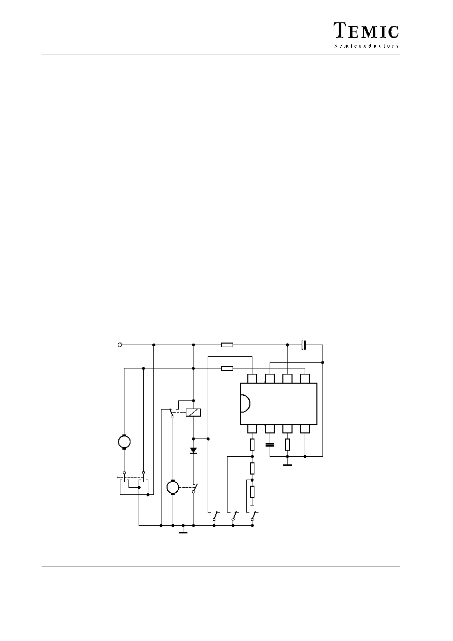
8
7
6
5
1
2
3
4
U840B
C
1
47
µ
F
1.4 k
R
3
C
2
100 n F
39 k
R
6
1.3 k
R
1
4.7 k
R
2
3
2
1
2
1
2
1
R
5
10 k
R
4
180
Park
switch
M
Wiper
motor
M
Water
pump
V
Batt
C
A
B
13286
Figure 3. Application circuit with interval and WIWA operation
U840B
TELEFUNKEN Semiconductors
Rev. A2, 03-Feb-97
5 (8)
Absolute Maximum Ratings
Parameters
Symbol
Value
Unit
Supply voltage
t = 60 s
t = 1 h
V
S
V
S
24
18
V
V
Ambient temperature range
T
amb
≠40 to +100
∞
C
Storage temperature range
T
stg
≠55 to +125
∞
C
max. junction temperature
T
J
150
∞
C
Thermal Resistance
Parameters
Symbol
Value
Unit
Junction ambient
DIP8
SO8
R
thJA
R
thJA
110
160
K/W
K/W
Electrical Characteristics
V
Batt
= 13.5 V, T
amb
= 25
∞
C, reference point ground (Pin 7) circuit with recommended external circuitry
Parameters
Test Conditions / Pin
Symbol
Min.
Typ.
Max.
Unit
Supply
Supply voltage range
V
S
9
16
V
Supply current, all push-
buttons open
I
6
3
mA
Undervoltage threshold
POR
V
6
4
V
Series resistance
R
V
180
W
Filter capacitance
C
S
47
mF
Internal Z-diode
V
6
14
V
INT input (Pin 1)
Protective diode
V
1
14
V
Internal capacitance
C
1
25
pF
External resistance
R
INT
1
k
W
Leakage resistance
R
L
40
60
k
W
PP input (Pin 4)
Protective diode
V
4
14
V
Internal capacitance
C
4
13
pF
Threshold
V
4
0.5 * V
S
V
Pull-down resistance
R
4
120
k
W
WASH-input (Pin 5)
Protective diode
V
5
14
V
Internal capacitance
C
5
25
pF
Threshold
V
5
0.5
V
S
V
Leakage resistance
R
L
10
k
W
Pull-down resistance
R
5
20
k
W
Relay output with limitation of short circuit current (Pin 8)
Saturation voltage 100 mA
V
8
1.0
V
Saturation voltage 200 mA
V
8
1.2
V
Relay coil resistance
R
REL
60
W

U840B
TELEFUNKEN Semiconductors
Rev. A2, 03-Feb-97
6 (8)
Parameters
Test Conditions / Pin
Symbol
Min.
Typ.
Max.
Unit
Output current
Normal operation
I
8
300
mA
Output pulse current
Load dump
I
8
1.5
A
Internal Z-diode
V
8
28
V
Short circuit threshold
I
8
500
mA
Oscillator input
Oscillator capacitance,
Pin 2 (
±
5%, TC MKT,
MKS2)
C
2
100
nF
Oscillator resistance, Pin 3
(
±
1% TC)
R
6
39
k
W
Oscillator frequency
f
0
320
Hz
Upper switching point
V
2
3
V
Lower switching point
V
2
1
V
Internal discharge resis-
tance
R
2
500
W
Times
External circuitry see oscillator input
Debouncing time CP, INT
t
1
67
110
ms
Interval turn-on time
t
2
300
450
ms
Interval pause
t
3
0.8
22
s
Turn-on delay
Wipe/ wash mode, PP to
GND
t
4
+ t
D
800
1000
ms
Dry wiping time
t
5
+ t
D
3400
4200
ms
Debouncing time short
circuit
t
6
6
11
ms
t
D
= debouncing time
1. Interval cycle time
t
2
+ t
3,1
1200
1500
ms
2. Interval cycle time
t
2
+ t
3,2
1980
2450
ms
1. Interval cycle time
t
2
+ t
3,3
4900
6100
ms
U840B
TELEFUNKEN Semiconductors
Rev. A2, 03-Feb-97
7 (8)
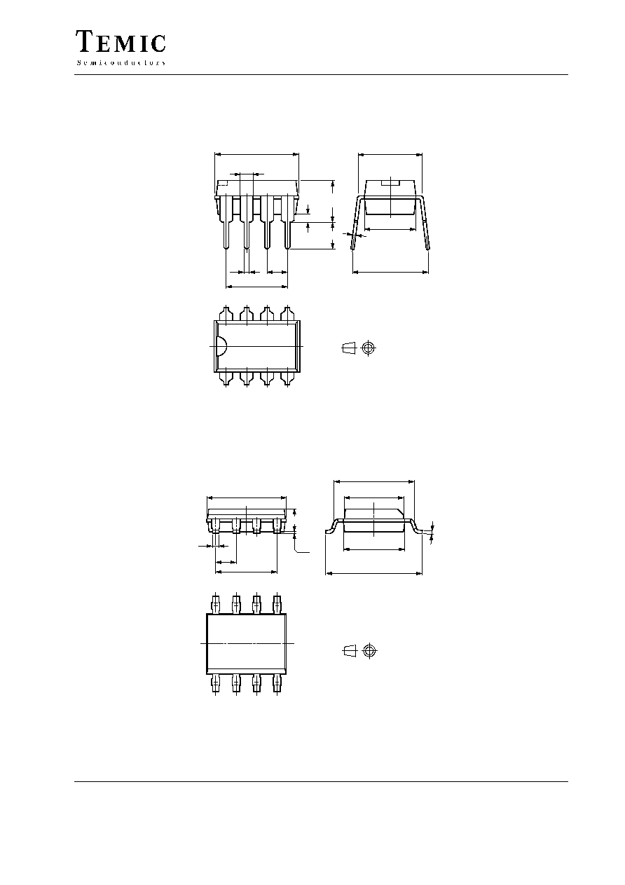
Package Information
13021
9.8
9.5
Package DIP8
Dimensions in mm
1.64
1.44
4.8 max
0.5 min
3.3
0.58
0.48
7.62
2.54
6.4 max
0.36 max
9.8
8.2
7.77
7.47
8
5
1
4
technical drawings
according to DIN
specifications
13034
technical drawings
according to DIN
specifications
Package SO8
Dimensions in mm
5.00
4.85
0.4
1.27
3.81
1.4
0.25
0.10
5.2
4.8
3.7
3.8
6.15
5.85
0.2
8
5
8
5

U840B
TELEFUNKEN Semiconductors
Rev. A2, 03-Feb-97
8 (8)
Ozone Depleting Substances Policy Statement
It is the policy of TEMIC TELEFUNKEN microelectronic GmbH to
1. Meet all present and future national and international statutory requirements.
2. Regularly and continuously improve the performance of our products, processes, distribution and operating systems
with respect to their impact on the health and safety of our employees and the public, as well as their impact on
the environment.
It is particular concern to control or eliminate releases of those substances into the atmosphere which are known as
ozone depleting substances ( ODSs ).
The Montreal Protocol ( 1987 ) and its London Amendments ( 1990 ) intend to severely restrict the use of ODSs and
forbid their use within the next ten years. Various national and international initiatives are pressing for an earlier ban
on these substances.
TEMIC TELEFUNKEN microelectronic GmbH semiconductor division has been able to use its policy of
continuous improvements to eliminate the use of ODSs listed in the following documents.
1. Annex A, B and list of transitional substances of the Montreal Protocol and the London Amendments respectively
2 . Class I and II ozone depleting substances in the Clean Air Act Amendments of 1990 by the Environmental
Protection Agency ( EPA ) in the USA
3. Council Decision 88/540/EEC and 91/690/EEC Annex A, B and C ( transitional substances ) respectively.
TEMIC can certify that our semiconductors are not manufactured with ozone depleting substances and do not contain
such substances.
We reserve the right to make changes to improve technical design and may do so without further notice.
Parameters can vary in different applications. All operating parameters must be validated for each customer
application by the customer. Should the buyer use TEMIC products for any unintended or unauthorized
application, the buyer shall indemnify TEMIC against all claims, costs, damages, and expenses, arising out of,
directly or indirectly, any claim of personal damage, injury or death associated with such unintended or
unauthorized use.
TEMIC TELEFUNKEN microelectronic GmbH, P.O.B. 3535, D-74025 Heilbronn, Germany
Telephone: 49 ( 0 ) 7131 67 2831, Fax number: 49 ( 0 ) 7131 67 2423