 | –≠–ª–µ–∫—Ç—Ä–æ–Ω–Ω—ã–π –∫–æ–º–ø–æ–Ω–µ–Ω—Ç: ADC180 | –°–∫–∞—á–∞—Ç—å:  PDF PDF  ZIP ZIP |

APPLICATIONS
∑ INERTIAL GUIDANCE
∑ TEST EQUIPMENT
∑ DATA ACQUISITION
∑ SCIENTIFIC INSTRUMENTS
∑ MEDICAL INSTRUMENTS
∑ WEIGHT SCALES
FEATURES
∑ 26 BIT RESOLUTION
∑ UP TO 2.5kHz CONVERSION RATES
∑ AUTO ZERO FUNCTION
∑ ±10.48 V INPUT RANGE
∑ 0.5ppm/∞C MAX. SCALE FACTOR ERROR
AND 2 ppm MAX. LINEARITY ERROR
(-55∞C to +125∞C).
∑ 8 BIT PARALLEL DATA BUS
∑ INTERNAL CRYSTAL CLOCK and
PRECISION REFERENCE
∑ LOW POWER CONSUMPTION: 0.4 WATTS
DESCRIPTION
The ADC180 is a 26 bit, charge balanced A/D
converter. Continuous sampling of 20 MHz and
conversion rates of up to 2.5 kHz make the converter
ideal for low frequency signal measurement. The
integration time is user selectable through an
external capacitor.
The ADC180 will continuously collect and average
integrations until the user requests data. Converter
resolution is dependent on the number of integration
cycles completed before the data is requested.
Converter resolution ranges from 13 - 26 bits.
In order to retain accuracy, internal calculations are
made at a 32 bit level. The output of the result is
also made at the 32 bit level. This makes it possible
to use a relatively high conversion rate and average
the data external to the converter without loss of
accuracy due to computation roundoff errors. For
inertial guidance systems, velocity information can
be obtained at a high rate without loss of position
accuracy.
The use of hybrid technology allows for separation
of sensitive analog circuitry from digital circuit
noise. This produces far superior accuracy over
monolithic A/D convertors.
The converter uses a proprietary, patented charge
balance modulator. It has an internal crystal clock,
microcontroller, precision reference, and patented
nonlinear temperature compensation network which
provides excellent electrical performance over
temperature.
The maximum scale factor drift is 0.5ppm/
o
C,
maximum offset drift of 0.1ppm/
o
C, and a maximum
nonlinearity over the mil. temp. range of 2 ppm.
The ADC180 is packaged in a 40 pin hermetic
TDIP and requires ±15V and +5V supplies. The
converter dissipates 450 mW and is available in
commercial and military grades.
ADC180DS REV H MAR 00
ADC180
Programmable
Integrating A/D Converter
THALER CORPORATION ∑ 2015 N. FORBES BOULEVARD ∑ TUCSON, AZ. 85745 ∑ (520) 882-4000
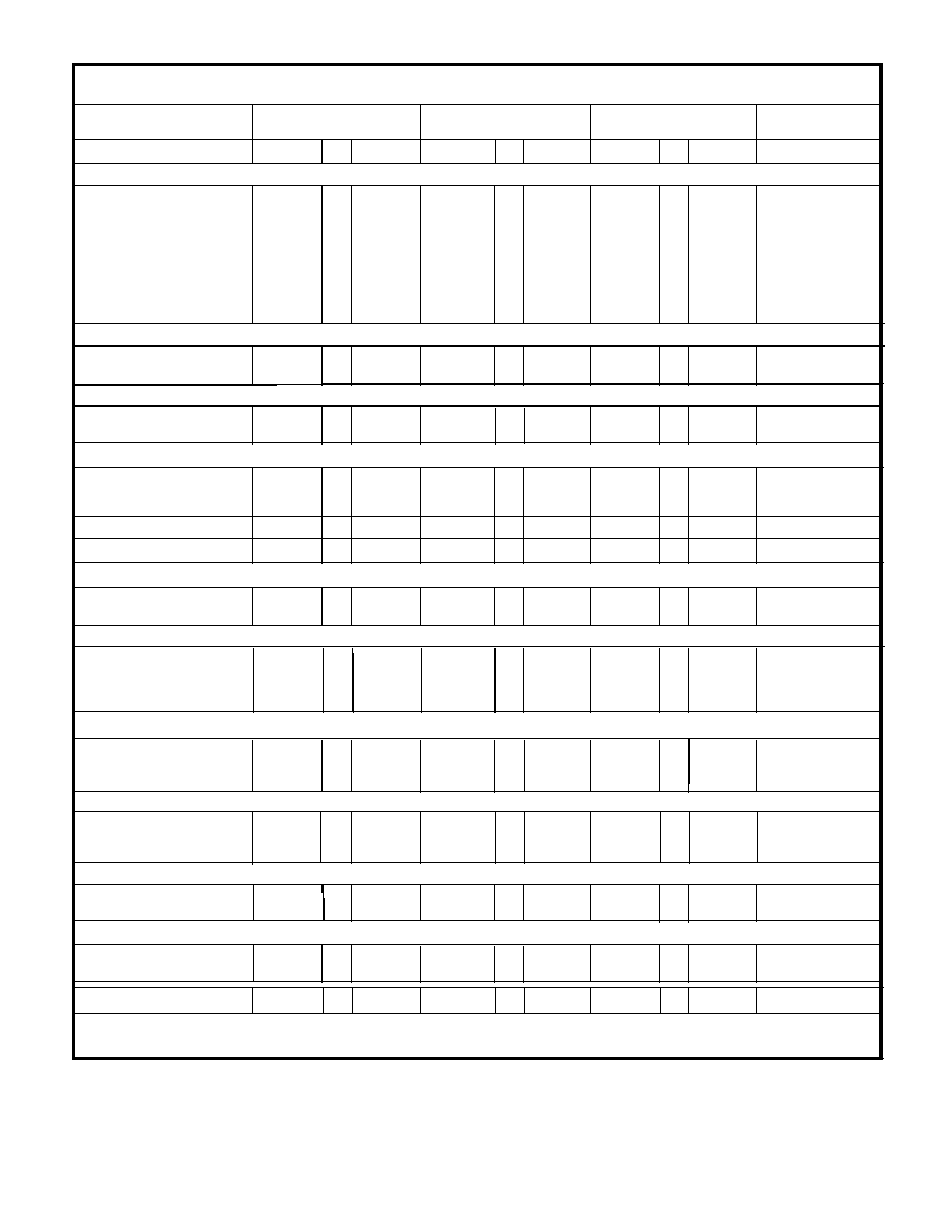
ELECTRICAL SPECIFICATIONS
MODEL
PARAMETER
ACCURACY
TEMPERATURE STABILITY
TIME STABILITY
ERROR ALL SOURCES
CONVERSION TIME
WARM-UP TIME
TEMPERATURE RANGE
DIGITAL OUTPUTS
DIGITAL INPUTS
POWER SUPPLY CURRENTS
POWER SUPPLY VOLTAGES
ANALOG INPUT CHARACTERISTICS
POWER SUPPLY REJECTION
Resolution
Input Equivalent Noise
Offset without Auto Zero
Offset with Auto Zero
Scale Factor Error
Noise (.1-10Hz) @ 10V
Nonlinearity
Normal Mode Rejection
Common Mode Rejection
Offset
Full Scale
Offset
Full Scale
MIN
MAX
TYP
MIN
MAX
TYP
MIN
MAX
TYP
ADC180C
ADC180CA
ADC180M
bits
µV
ppm FS
ppm FS
ppm FS
µVpp
ppm FS
dB
dB
.25
6
1
*
*
*
*
*
*
*
*
*
*
60
80
*
*
*
*
0.2
0.1
*
1.0
0.5
*
ppm/
o
C
ppm/
o
C
0.1
2
ppm/24 hrs.
ppm/month
.0005, 2
.0003, 2
%, +/- counts
24 hrs, +/- 1 Deg. C Amb.
90 days, +/- 5 Deg. C Amb.
1 year, +/- 5 Deg. C Amb.
.0010, 2
.0008, 2
*
.0015, 2
.0013, 2
%, +/- counts
%, +/- counts
*
*
ms
*
5
*
*
*
minutes
+Vcc, -Vee
5 VDC
80
80
*
*
dB
*
*
dB
Low
High
Low
High
-25
85
*
*
-55
125
V
V
V
V
0.8
*
*
4.0
*
*
4.0
*
*
0.8
*
*
+Vcc
23
*
*
mA
-Vee
24
*
*
mA
+Vdd
42
*
*
mA
+Vcc
-Vee
+Vdd
+14.5
+15
+15.5
*
*
*
*
*
*
*
*
*
*
*
*
*
*
*
*
*
*
V
-14.5
-15
-15.5
V
+4.5
+5
+5.5
V
Input Range
-10.485760
+10.485755
3
*
*
*
*
*
*
*
*
V
Bias Current
1.2
*
*
nA
Input Impedance
Max. Input Voltage
200
*
*
GO
2
0.5
50
*
* Same as ADC180C
Notes: 1) 60 Cycle 2) ( Max-Min Value) - Noise(0.1-10Hz)
ADC180
(Vcc = +15V, Vee = -15V, Vdd = + 5V, TA = +25
o
C)
*
*
*
*
4
1
100
2
(1)
o
C
(2)
26
*
*
3200
0.250
*
*
13
*
*
ADC180DS REV H MAR 00
V
-Vee
+Vcc
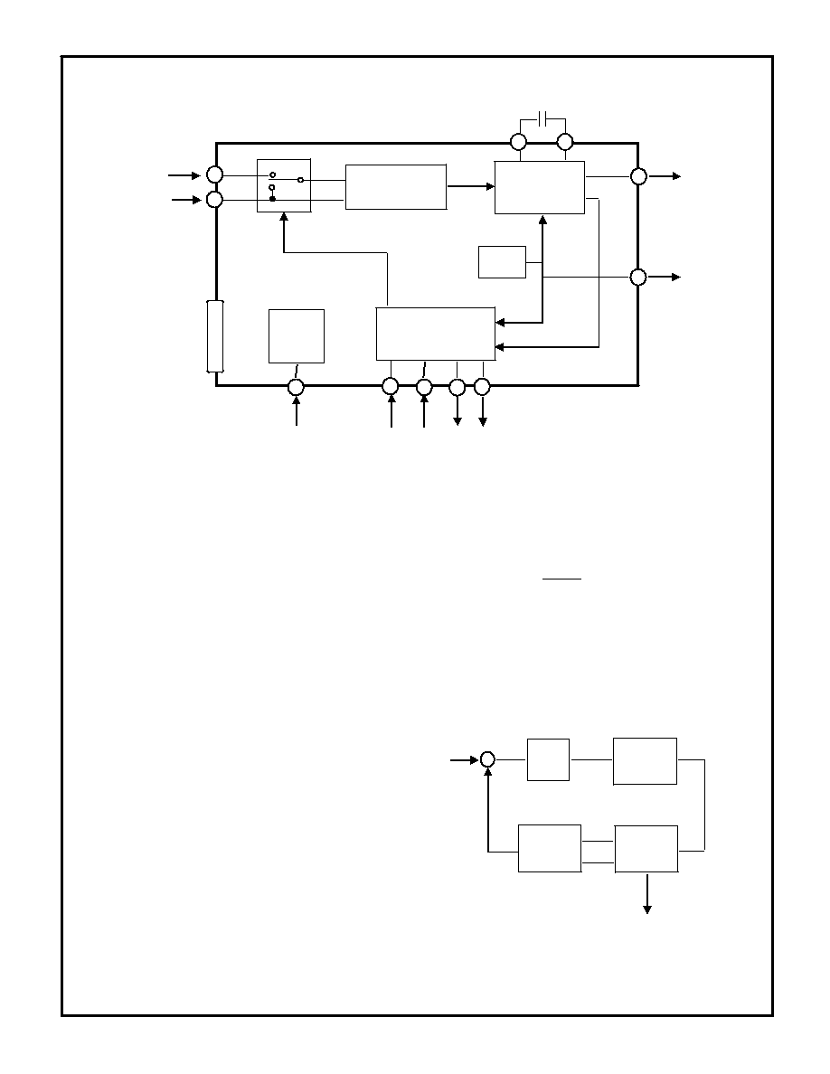
THEORY OF OPERATION
The ADC180 uses a differential input to improve
accuracy. To measure single source voltages,
V
low
should be connected to the ground point of the
source voltage to be measured. In figure 1, the
switch is shown in the normal operating mode
connecting
V
hi
and
V
low
to the differential input of
the transadmittance amplifier. For an autozero
cycle,
V
hi
is disconnected and the input to the
amplifier is shorted.
The charge balance modulator (figure 2) uses a
proprietary patented architecture to achieve the
high accuracy of the ADC180 without any error
correction method other than autozero. This
enables the converter to sample the output of the
transadmittance amplifier continuously at a
sampling rate of 20 MHz. This is important for
applications like inertial guidance systems where
Auto Zero Switch
Charge Balance
Modulator
Microprocessor
Output
Buffer
Crystal
Clock
Transadmittance
Amplifier
V
hi
V
low
Auto
Zero
Data
Request
Status
Lines
Output Enable
Data
Output
Ô
Ô
13
.
.
.
20
21
29
22
23
24
34
35
39
40
FIGURE 1. BLOCK DIAGRAM
Bidirectional
Curent
Source
Direction
Switch
Bilevel
Comparator
Figure 2. Patented Charge Balance Modulator
The conversion result between two consecutive
data request inputs at times t
1
and t
2
is
mathematically represented by the equation
Data
Output
I
IN
ADC180DS REV H MAR 00
Duty Cycle
Test Point
3
20MHz clock output
26
The converter provides two 32 bit data words with
the first word containing t
2
-t
1
and the second word
containing
-
=
2
1
1
2
1
t
t
inp
iav
dt
V
t
t
V
dt
V
t
t
inp
2
1
dt
V
t
t
inp
2
1
must be measured without any loss of time
increments. The output of the charge balance
modulator is in the form of a pulse width
modulation signal. The internal microprocessor
provides all control functions and digital signal
processing.
The converter also has an internal crystal clock to
avoid phase jitter errors and a tristate output
buffer for easy interface with bus based systems.
For the data output timing see figures 5 and 6.
CONNECTING THE ADC180
DUTY CYCLE OUTPUT (pin 3)
This logic level output allows monitoring of the
integration cycle and is usually used for timing
purposes.
POWER SUPPLIES (pins 4-7)
The ADC180 has internal 0.1µF decoupling
capacitors for all power supply inputs. This is
sufficient for applications with relatively short power
supply leads (approx. 5") or if additional capacitors
are located on the circuit board. External capacitors
of 10 µF on the ±15V inputs and 33 µF on the +5V
input is recommended for applications with longer
power supply leads.
GROUND (pin7)
Since ground noise can result in a loss of accuracy,
the ground connection should be made as solid as
possible. Use of a ground plane is a good approach
to maintain the full accuracy of the ADC180.
OUTPUT DATA LINES (pins 13-20)
The parallel output data is available on pins 13-20.
Pin 20 is the Most Significant Bit and pin 13 the
Least Significant Bit. The data lines go to a high
impedance state when the Output Enable line is at a
logic 1 level.
ANALOG INPUTS (pins 39,40)
The differential analog inputs are buffered by
op amps and have a common mode rejection of
approximately 80dB minimum. To maintain the full
accuracy of the ADC180 it is recommended to
maintain the input to analog low to less than
0.1VDC. To avoid differential noise pickup, parallel
adjacent lines should be used for the analog inputs
on PC boards and shielded lines outside of the PC
connections.
CAPACITOR (pin 34, 35)
The only external component required to operate
the ADC180 is a capacitor which sets the
integration time. A 0.082 µF capacitor results in an
integration time of approximately 250 µs. For 2,000
µs a 0.68µF capacitor is required. The relationship
is linear for intermediate capacitor values.
The main parameter affected by shorter conversion
times is bias stability over temperature.
Polystyrene, mylar, or polycarbonate capacitors are
recommended.
AUTO ZERO / RESET (pin 29)
A logic 0 on this input will autozero the ADC180 by
internally connecting the analog high to analog low.
Since the internal microprocessor is reset, the
ADC180 is not functional during this time
(approximately 1s). S
1
will go to logic 1 indicating
that no data is available. After completing the
autozero function, S
1
will return to logic 0 and the
ADC will begin collecting data.
20MHz CLOCK OUTPUT (pin 26)
Output of the internal crystal oscillator.
STATUS LINES (pins 23, 24)
These lines indicate the present state of the ADC.
After a data request has been received and the
current integration cycle is complete, the ADC will
output the data collected subsequent to the
previous data request. S
1
will go to logic 1 to
acknowledge the data request. The 8 bytes of data
will be placed on the data bus sequentially. A logic
1 on S
0
indicates valid data on the data bus. After
the data has been transmitted, S
1
will return to
logic 0.
DATA REQUEST (pin 22)
A logic 0 on this line initiates a data transfer
sequence.
OUTPUT ENABLE (pin 21)
A logic 0 on this line enables outputs D0 - D7.
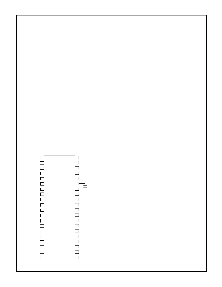
NC= Factory test points, do not connect to these pins.
Vee (-15V)
Vcc (+15V)
Vdd (+5V)
(TOP VIEW)
ADC180
1
2
3
4
5
6
7
8
9
10
11
12
13
14
15
16
17
18
19
20
40
39
38
37
36
35
34
33
32
31
30
29
28
27
26
25
24
23
22
21
N.C.
Duty Cycle Output
N.C.
N.C.
N.C.
N.C.
N.C.
N.C.
20MHz CLOCK OUTPUT
N.C.
N.C.
N.C.
D0
D1
D2
D5
D4
D3
D6
D7
GND
ANALOG LOW
ANALOG HIGH
/AUTO ZERO / RESET
S1
S0
/DATA REQUEST
/OUTPUT ENABLE
CAPACITOR
FIGURE 3. EXTERNAL CONNECTIONS
ADC180DS REV H MAR 00
N.C.
N.C.
N.C.
N.C.
N.C.
N.C.
N.C.
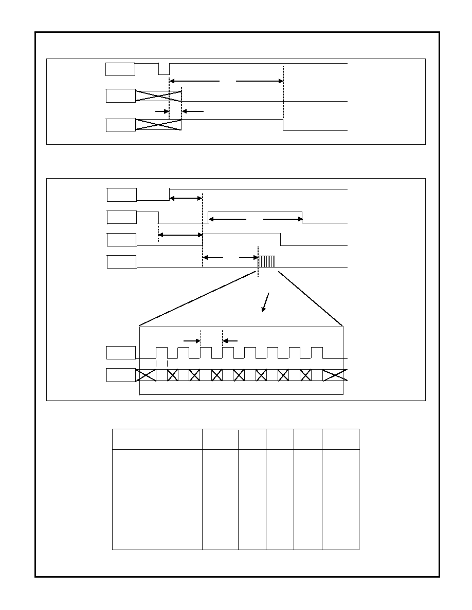
TIMING DIAGRAMS
FIGURE 4. AUTO ZERO TIMING
FIGURE 5. DATA REQUEST CYCLE TIMING
S1
S0
AutoZero
*
*
t
AZ
t
TS
t
AC
* Data Request at logic 1, output enable (don't care)
/DR
t
DD
t
DRA
t
NDR
FIGURE 6. TIMING TABLE
AutoZero request
Autozero Cycle
port TriState time
Data Request Acknowledge
S1 Response after duty cycle
Data Delay
time before Next Data Request
Data Valid
Data Cycle
t
AZ
t
AC
t
TS
t
DRA
t
S1R
t
DD
t
NDR
t
DV
t
DC
100
*
27
0
30
50
1
2
1.3
*
34
ns
s
ms
µs
µs
µs
µs
µs
* T
DRA
must be either 1 integration cycle minimum or until S1 goes high.
SIGNAL SYMBOL MIN TYP MAX UNITS
ADC180DS REV H MAR 00
t
S1R
duty cycle
S1
S0
S0
D0 - D7
t
DV
t
DC
enlarged detail
data on D0 - D7
valid upon rising
edge of S0