 | –≠–ª–µ–∫—Ç—Ä–æ–Ω–Ω—ã–π –∫–æ–º–ø–æ–Ω–µ–Ω—Ç: 1206S | –°–∫–∞—á–∞—Ç—å:  PDF PDF  ZIP ZIP |
THAT Corporation; 45 Sumner Street; Milford, Massachusetts 01757-1656; USA
Tel: +1 (508) 478-9200; Fax: +1 (508) 478-0990; Web: www.thatcorp.com
THAT 1200, 1203, 1206
Description
The THAT 1200 series of InGenius balanced
line receivers are designed to overcome a serious
limitation of conventional balanced input stages
-- notoriously poor common mode rejection in
real world applications. While conventional input
stages may exhibit good rejection characteristics
in the lab and on paper, they perform poorly
when fed from even slightly unbalanced source
impedances -- a common situation in almost any
pro sound environment.
Developed by Bill Whitlock of Jensen Trans-
formers, the patented InGenius input stage uses a
unique bootstrap circuit to raise its common-
mode input impedance into the megohm range,
but without the noise penalty that comes from
high-valued resistors. InGenius line receivers
maintain their high CMRR over a wide range of
source impedance imbalances -- even when fed
from single-ended sources.
T H A T
C o r p o r a t i o n
InGenius
‚
High-CMRR
Balanced Input Line Receiver
FEATURES
∑
High common-mode rejection
(typical 90 dB at 60 Hz) maintained
under real-world conditions
∑
Excellent solution for hum and
groundloop suppression
∑
Transformer-like noise rejection in
an 8-pin IC, at fraction of
transformer cost and size
APPLICATIONS
∑
Balanced input stages
∑
Summing amplifiers
∑
Transformer front-end
replacements
∑
ADC front-ends
+1
+1
R1
R2
R3
R4
IN-
IN+
REF
CM OUT
Vcc
Vee
Vout
+1
-
+
CM IN
Cb
R5
Ra
Rb
Rc
Rd
OA1
OA2
OA3
OA4
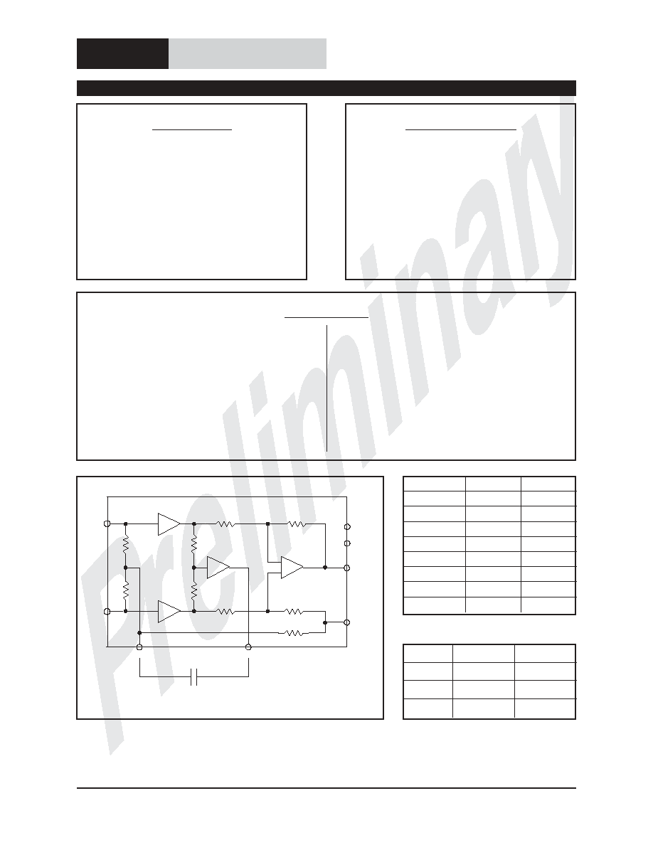
Figure 1. THAT1200-series equivalent circuit diagram
Pin Name
DIP Pin
SO Pin
Ref
1
3
In-
2
4
In+
3
5
Vee
4
6
CM In
5
11
Vout
6
12
Vcc
7
13
CM Out
8
14
Table 1. 1200-series pin assignments
Gain
Plastic DIP
Plastic SO
0 dB
1200P
1200S
-3 dB
1203P
1203S
-6 dB
1206P
1206S
Table 2. Ordering information
Protected under U.S. Patent No. 5,568,561 and other patents pending.
InGenius‚ is a trademark of THAT Corporation.
600033 Rev 0A

THAT Corporation; 45 Sumner Street; Milford, Massachusetts 01757-1656; USA
Tel: +1 (508) 478-9200; Fax: +1 (508) 478-0990; Web: www.thatcorp.com
Page 2
InGenius Balanced Line Receiver
Preliminary Information
Absolute Maximum Ratings (T
A
= 25∞C)
Positive Supply Voltage (V
CC
)
+18 V
Power Dissipation (P
D
) (T
A
= 75∞C)
TBD mW
Negative Supply Voltage (V
EE
)
-18 V
Operating Temperature Range (T
OP
)
0 to +70∞C
Positive Input Voltage (V
IN+
)
+18 V
Storage Temperature Range (T
ST
)
-40 to +125∞C
Negative Input Voltage (V
IN-
)
-18 V
Junction Temperature (T
J
)
150∞C
Output Short-Circuit Duration (t
SH
)
Continuous
Lead Temperature (Soldering 60 seconds)
TBD ∞C
Electrical Characteristics
2
Parameter
Symbol
Conditions
Min
Typ
Max
Units
Supply Current
I
CC
No signal
--
4.7
8.0
mA
Input Bias Current
I
B
No signal; Either input
--
700
1,400
nA
connected to GND
Input Offset Current
I
B-OFF
No signal
--
--
±140
nA
Input Offset Voltage
V
OFF
No signal
--
--
10
mV
Input Voltage Range
V
IN-CM
Common mode
±12.5
±13.0
--
V
V
IN-DIFF
Differential (equal and opposite swing)
THAT 1200
21.0
21.5
--
dBu
THAT 1203
24.0
24.5
--
dBu
THAT 1206
24.0
24.5
--
dBu
Input Impedance
Z
IN-DIFF
Differential
48.0
k
W
Z
IN-CM
Common mode
with bootstrap
60 Hz
10.0
M
W
20 kHz
3.2
M
W
no bootstrap
60 Hz
36.0
k
W
20 kHz
36.0
k
W
Recommended Operating Conditions
Parameter
Symbol
Conditions
Min
Typ
Max
Units
Positive Supply Voltage
V
CC
+3
+18
V
Negative Supply Voltage
V
EE
-3
-18
V
SPECIFICATIONS
1
1. All specifications are subject to change without notice.
2. Unless otherwise noted, T
A
=25∞C, V
CC
= +15V, V
EE
= -15V
3. 0 dBu = 0.775Vrms.

THAT Corporation; 45 Sumner Street; Milford, Massachusetts 01757-1656; USA
Tel: +1 (508) 478-9200; Fax: +1 (508) 478-0990; Web: www.thatcorp.com
600033 Rev 0A
Page 3
Preliminary Information
Electrical Characteristics (Cont'd)
Parameter
Symbol
Conditions
Min
Typ
Max
Units
Common Mode Rejection
CMR
1
Matched source impedances; V
CM
= ±10V
DC
70
90
--
dB
60 Hz
70
90
--
dB
20 kHz
--
85
--
dB
Common Mode Rejection
CMR
2
600
W unmatched source impedances
4
; V
CM
= ±10V
60 Hz
--
70
--
dB
20 kHz
--
65
--
dB
Power Supply Rejection
5
PSR
At 60 Hz, with V
CC
= -V
EE
THAT1200
--
82
--
dB
THAT1203
--
80
--
dB
THAT1206
--
80
--
dB
Power Supply Rejection
6
PSR
CM
At CM output, at 60 Hz
--
63
--
dB
Total Harmonic Distortion
THD
V
IN-DIFF
= 10 dBV; BW = 20 kHz; f = 1 kHz
RL =2 k
W
--
0.0005
--
%
Output Noise
e
n(OUT)
BW = 20 kHz
THAT1200
--
-106
--
dBu
THAT1203
--
-105
--
dBu
THAT1206
--
-107
--
dBu
Output Noise
e
nCM(OUT)
At CM output
--
-106
--
dBu
Slew Rate
SR
R
L
= 10 k
W; C
L
= 300 pF
7*
12
--
V/µs
Slew Rate
SR
CM
With CM input signal
12.5*
21
--
V/µs
R
Lcm
= 10 k
W; C
Lcm
= 50 pF
Small Signal Bandwidth
BW
-3dB
R
L
= 10 k
W; C
L
= 10 pF
THAT1200
--
22
--
MHz
THAT1203
--
27
--
MHz
THAT1206
--
34
--
MHz
R
L
= 2 k
W; C
L
= 300 pF
THAT1200
--
17
--
MHz
THAT1203
--
18
--
MHz
THAT1206
--
20
--
MHz
Small Signal Bandwidth
BW
CM-3dB
At CM output; R
Lcm
= 10 k
W
C
Lcm
= 10 pF
--
20
--
MHz
C
Lcm
= 50 pF
--
18
--
MHz
Output Gain Error
G
ER(OUT)
f = 1 kHz; R
L
= 2 k
W
--
0
±0.05
dB
Output Voltage Swing
V
O
At max differential input
THAT1200
21
21.5
--
dBu
THAT1203
21
21.5
--
dBu
THAT1206
18
18.5
--
dBu
4. See test circuit in Figure 2.
5. Defined with respect to the differential gain.
6. Defined with respect to the common mode gain between any input and common mode output.
* Guaranteed by design
Applications
RFI Protection
Figure 3 shows the THAT 1200 configured with
robust RFI input protection.
In applications where
RFI rejection is of less concern, the circuit shown Fig-
ure 4 provides a less aggressive approach.
Bootstrap coupling capacitor
Referring to Figure 3, electrolytic capacitor Cb
provides the feedback path for the boostrap circuit.
The capacitor value is chosen to be high enough to
present a sufficiently small impedance to signals at
the low end of the audio spectrum. Its voltage rating
is dependent on the topology of the surrounding cir-
cuitry, as described in the following paragraphs.
AC signals presented to the input stage cause the
two ends of capacitor Cb to swing in tandem so that
virtually no voltage appears across the capacitor.
Consequently, capacitors with small DC working volt-
ages may be used when the previous stage is AC cou-
pled to the input of the THAT 1200.
THAT Corporation; 45 Sumner Street; Milford, Massachusetts 01757-1656; USA
Tel: +1 (508) 478-9200; Fax: +1 (508) 478-0990; Web: www.thatcorp.com
Page 4
InGenius Balanced Line Receiver
Preliminary Information
Electrical Characteristics (Cont'd)
Parameter
Symbol
Conditions
Min
Typ
Max
Units
Output Short Circuit Current
I
SC
R
L
= R
Lcm
= 0
W
--
±25
--
mA
I
CMSC
At CM output
--
±10
--
mA
Minimum Resistive Load
R
Lmin
2
--
--
k
W
R
LCMmin
At CM output
10
--
--
k
W
Maximum Capacitive Load
C
Lmax
--
--
300
pF
C
LCMmax
At CM output
--
--
50
pF
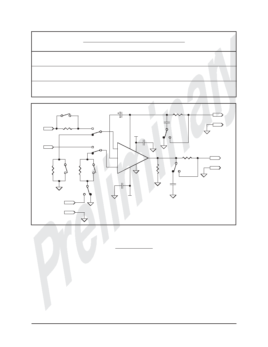
1
In-
2
In+
3
CMin
5
4
8
7
Out
6
U1
THAT120x
Cb
100u
C1
56p
C2
300p
C3
100n
C4
100n
R1
200k
R2
200k
R3
600R
R4
2k
R5
100R
R6
100R
Vcc
Vee
In-
In+
Ext. DC Source
CM Out
Main Out
Gnd
Gnd
Gnd
CMout
Vcc
Ref
Vee
Figure 2. THAT1200-series test circuit
If, however, there is the possibility of a DC voltage
appearing across the inputs of the line receiver, a
portion of that voltage will appear directly across the
terminals of capacitor Cb. In that case, choose the
capacitor's voltage rating so that it is capable of han-
dling the expected level of DC voltage. If the polarity
of the DC voltage is unknown, or may swing to either
polarity, the use of a non-polarized electolytic is
highly recommended.
THAT Corporation; 45 Sumner Street; Milford, Massachusetts 01757-1656; USA
Tel: +1 (508) 478-9200; Fax: +1 (508) 478-0990; Web: www.thatcorp.com
600033 Rev 0A
Page 5
Preliminary Information
5
IN-
2
IN+
3
8
4
1
7
6
OUT
CM
IN
CM
OUT
REF
VCC
VEE
U1
Cb
220uF
5 4
3 1
2
2
3
1
J1
XLR-F
Vcc
Vee
OUT
C2
100pF NPO
C1
100pF NPO
+
Vcc
Vee
D1
12V
D2
12V
D4
D3
D6
D5
Figure 4. THAT1200P showing simplified RFI protection scheme
5
IN-
2
IN+
3
8
4
1
7
6
OUT
CM
IN
CM
OUT
REF
VCC
VEE
U1
R3
4k7
Cb
220uF
C2
470pF
C3
470pF
C4
100pF
R1
R2
5 4 3 1
2
2
3
1
J1
XLR-F
Vcc
Vee
OUT
100R
100R
(see text)
optional RFI protection
+
Vcc
Vee
D1
12V
D2
12V
D4
D3
D6
D5
Figure 3. THAT1200P typical application circuit