
THAT Corporation; 45 Sumner St., Milford, Massachusetts; 01757-1656; USA
Tel: +1 (508) 478-9200; Fax: +1 (508) 478-0990; Web: www.thatcorp.com
T H A T
C o r p o r a t i o n
1
2
3
4
5
6
7
SUB
NC
8
9
10
11
12
13
14
Q2 Q1
Q4 Q3
Figure 1. Pin
Configuration
0.750±0.004
(19.05±0.10)
0.25±.004
(6.35±0.10)
0.32 Max.
(8.13)
0.060
(1.52)
0.075
(1.91)
0.10 Typ.
(2.54)
0.018
(0.46)
0.125±0.004
(3.18±0.10)
Typ.
1
0.010
(0.25)
Figure 2. Dual-In-Line Package Outline
Quad Low-Noise
NPN Transistor Array
THAT100
FEATURES
∑
Four Matched NPN Transistors
∑
Low noise -- 0.8
nV
Hz
∑
High Speed -- 350 MHz f
t
∑
Excellent Matching -- 500
µ
V typ
∑
Dielectrically Isolated
∑
25 V V
CEO
APPLICATIONS
∑
Microphone Preamplifiers
∑
Tape Head Preamplifiers
∑
Current Sources
∑
Current Mirrors
∑
Log/Antilog Amplifiers
∑
Multipliers
DESCRIPTION
THAT100 is a quad, large-geometry monolithic
NPN transistor array which combines low noise, high
speed and excellent parametric matching. The large
geometry typically results in 30
base spreading re-
sistance, producing 0.8
nV Hz
voltage noise. This
makes these parts an excellent choice for low-noise
amplifier input stages.
Fabricated on a Complementary Bipolar Dielec-
trically Isolated process, all four transistors are elec-
trically isolated from each other by a layer of oxide.
The resulting low collector-to-substrate capacitance
produces a typical f
t
of 350 MHz, for AC perfor-
mance similar to 2N3904-class devices. The dielec-
tric isolation also minimizes crosstalk and provides
complete DC isolation.
Substrate biasing is not required for normal op-
eration, though the substrate should be grounded to
optimize speed. The one-chip construction assures
excellent parameter matching and tracking over
temperature.
0.050
(1.27)
Typ
0.245
(6.2)
Max
0.157
(3.99)
Max
0.018 (0.46)
Max
0.344 (8.74)
Max
0.069
(1.75)
Max
0.010
(0.25)
Max
1
Figure 3. Surface Mount Package Outline
THAT Corporation; 45 Sumner St., Milford, Massachusetts; 01757-1656; USA
Tel: +1 (508) 478-9200; Fax: +1 (508) 478-0990; Web: www.thatcorp.com
Rev. 07/25/00
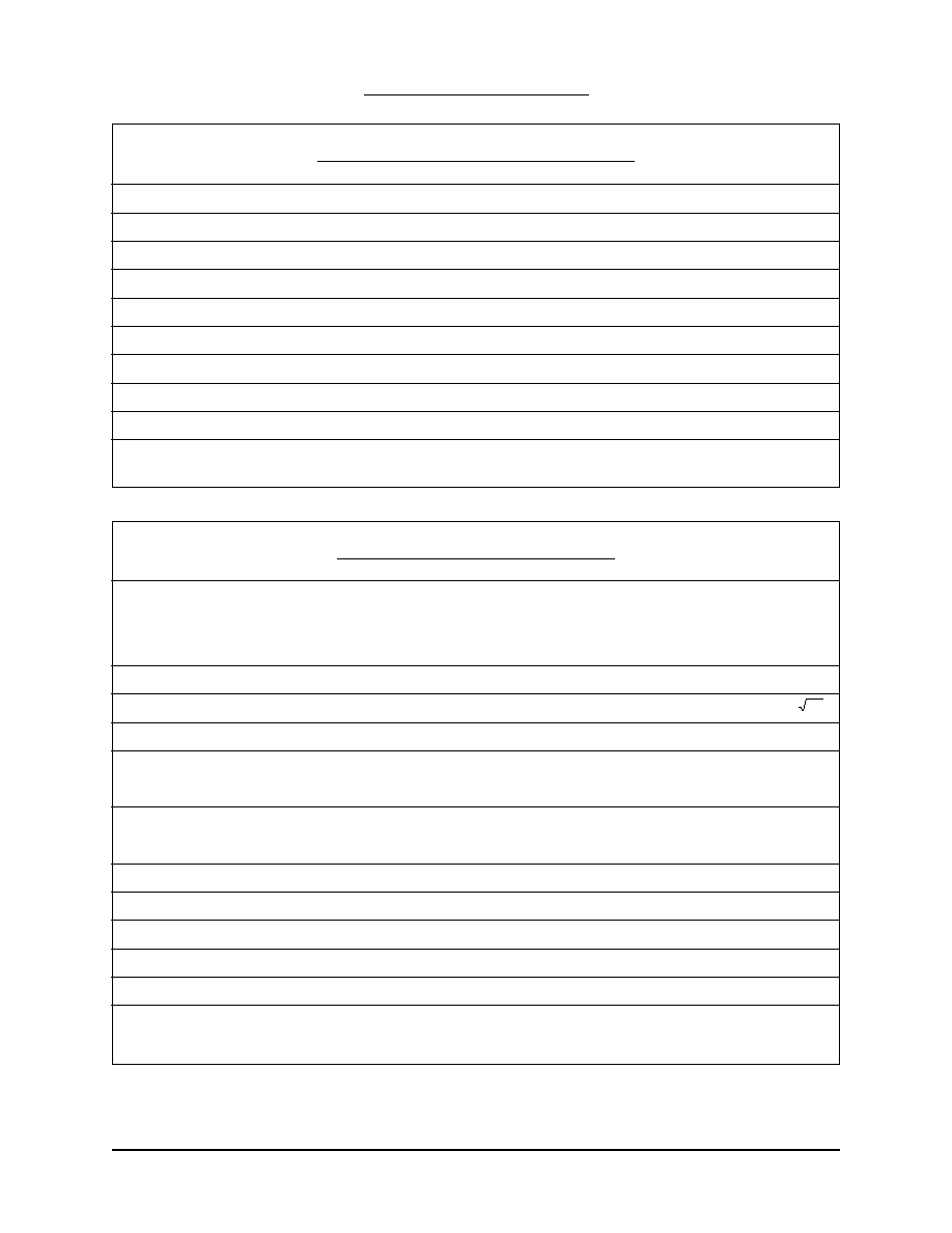
SPECIFICATIONS
1
Maximum Ratings (T
A
= 25
∞
C)
Parameter
Symbol
Conditions
Min
Typ
Max
Units
Collector-Emitter Voltage
BV
CEO
I
C
= 1 mAdc, I
B
= 0
25
35
V
Collector-Base Voltage
BV
CBO
I
C
= 10
µ
Adc, I
E
= 0
25
35
V
Emitter-Base Voltage
BV
EBO
I
E
= 10
µ
Adc, I
C
= 0
5
V
Collector-Collector Voltage
BV
CC
±
100
±200
V
Emitter-Emitter Voltage
BV
EE
±
100
±200
V
Collector Current
I
C
10
20
mA
Emitter Current
I
E
10
20
mA
Operating Temperature Range
T
A
0
70
∞
C
Maximum Junction Temperature T
JMAX
150
∞C
Storage Temperature
T
STORE
-45
125
∞C
Electrical Characteristics
2
Parameter
Symbol
Conditions
Min
Typ
Max
Units
Current Gain
h
fe
V
CB
= 10 V
I
C
= 1 mA
60
100
I
C
= 10
µ
A
60
100
Current Gain Matching
h
fe
V
CB
= 10 V, I
C
= 1 mA
--
5
--
%
Noise Voltage Density
e
N
V
CB
= 10 V, I
C
= 1 mA, 1 kHz
--
0.8
--
nV / Hz
Gain-Bandwidth Product
f
t
I
C
= 1 mA, V
CB
= 10 V
350
MHz
V
BE
(V
BE1
-V
BE2
; V
BE3
-V
BE4
)
V
OS
I
C
= 1 mA
--
±
0.5
±
3
mV
I
C
= 10
µ
A
--
±
0.5
±
3
mV
I
B
(I
B1
-I
B2
; I
B3
-I
B4
)
I
OS
I
C
= 1 mA
--
±
500
±
1500
nA
I
C
= 10
µ
A
--
±
5
±
15
nA
Collector-Base Leakage Current
I
CBO
V
CB
= 25 V
--
25
--
pA
Bulk Resistance
r
BE
V
CB
= 0 V, 10
µ
A < I
C
< 10mA
--
2
--
Base Spreading Resistance
r
bb
V
CB
= 10 V, I
C
= 1mA
--
30
--
Collector Saturation Voltage
V
CE(SAT)
I
C
= 1 mA, I
B
= 100
µ
A
--
0.05
V
Output Capacitance
C
OB
V
CB
= 10 V, I
E
= 0 mA, 100 kHz
3
pF
Collector-Collector Capacitance
Q
1
/Q
2
; Q
3
/Q
4
C
CC
V
CC
= 0 V, 100 kHz
0.7
pF
1. All specifications subject to change without notice.
2. Unless otherwise noted, T
A
=25∞C.