 | –≠–ª–µ–∫—Ç—Ä–æ–Ω–Ω—ã–π –∫–æ–º–ø–æ–Ω–µ–Ω—Ç: THAT1243 | –°–∫–∞—á–∞—Ç—å:  PDF PDF  ZIP ZIP |

THAT Corporation; 45 Sumner Street; Milford, Massachusetts 01757-1656; USA
Tel: +1 (508) 478-9200; Fax: +1 (508) 478-0990; Web: www.thatcorp.com
T H A T
C o r p o r a t i o n
THAT 1240, 1243, 1246
FEATURES
∑
High CMRR: typically 90dB at 60Hz
∑
Wide bandwidth and high slew rate
∑
Low distortion and low noise
∑
Available in 0 dB, -3 dB, and -6 dB
versions
∑
Pin compatible with SSM2143 and
INA137
APPLICATIONS
∑
Balanced Audio Line Receivers
∑
Summing Amplifiers
∑
Differential Amplifiers
∑
Current Shunt Monitors
∑
Ground Loop Eliminator
Description
The THAT 124x series of precision differential
amplifiers are designed primarily for use as audio
balanced line receivers. Gains of 0 db, -3 dB, and
-6 dB are available to suit various applications re-
quirements.
The THAT 1246 is drop-in compatible with
the Burr-Brown INA137 and Analog Devices
SSM2143, while the THAT 1240 is drop-in com-
patible with the SSM2140.
All devices exhibit 90 dB of typical com-
mon-mode rejection, slew rates of 12 V/
ms, a
20MHz bandwidth, and 0.0006% THD. Both sur-
face-mount and DIP packages are available.
The THAT 124x family are laser-trimmed to
obtain the precision resistor matching needed for
high CMR performance. Fashioned in THAT Cor-
poration's proprietary dielectric isolation (DI)
process, the THAT 124x series provides the sonic
benefit of discrete designs, with the compact size,
reliability, matching, and thermal tracking of a
fully integrated solution.
Sense
Vout
Ref
Vcc
Vee
In+
In-
NC
Figure 1. THAT1240-series equivalent circuit diagram
Gain
Plastic DIP
Plastic SO
0 dB
1240P
1240S
-3 dB
1243P
1243S
-6 dB
1246P
1246S
Table 2. Ordering information
Pin Name
DIP Pin
SO Pin
Ref
1
1
In-
2
2
In+
3
3
Vee
4
4
Sense
5
5
Vout
6
6
Vcc
7
7
NC
8
8
Table 1. 1240 Series pin assignments
Balanced Line Receiver ICs
THAT Corporation; 45 Sumner Street; Milford, Massachusetts 01757-1656; USA
Tel: +1 (508) 478-9200; Fax: +1 (508) 478-0990; Web: www.thatcorp.com
Page 2
Balanced Line Receiver ICs
Preliminary Information
SPECIFICATIONS
1
Absolute Maximum Ratings (T
A
= 25∞C)
Positive Supply Voltage (V
CC
)
+18 V
Power Dissipation (P
D
) (T
A
= 75∞C)
TBD mW
Negative Supply Voltage (V
EE
)
-18 V
Operating Temperature Range (T
OP
)
0 to +70∞C
Storage Temperature Range (T
ST
)
-40 to +125∞C
Junction Temperature (T
J
)
150∞C
Output Short-Circuit Duration (t
SH
)
Continuous
Lead Temperature (Soldering 60 seconds)
TBD ∞C
Positive Input Voltage (Ref, Sense)
+18 V
Negative Input Voltage (Ref, Sense)
-18 V
THAT1240
THAT1243
THAT1246
Positive Input Voltage (In+,In-)
Vcc x 2
Vcc x 2.4
Vcc x 3
Negative Input Voltage (In+, In-)
Vee x 2
Vee x 2.4
Vee x 3
Recommended Operating Conditions
Parameter
Symbol
Conditions
Min
Typ
Max
Units
Positive Supply Voltage
V
CC
+2.2
+18
V
Negative Supply Voltage
V
EE
-2.2
-18
V
Electrical Characteristics
2
Parameter
Symbol
Conditions
Min
Typ
Max
Units
Supply Current
I
CC
No signal
--
2.1
3.4
mA
Input Voltage Range
V
IN-DIFF
Differential (equal and opposite swing)
THAT1240 (0 dB gain)
--
21.5
--
dBu
3
THAT1243 (-3 dB gain)
--
24.5
--
dBu
THAT1246 (-6 dB gain)
--
27.5
--
dBu
V
IN-CM
Common mode
THAT1240 (0 dB gain)
--
27.5
--
dBu
THAT1243 (-3 dB gain)
--
29.1
--
dBu
THAT1246 (-6 dB gain)
--
31.0
--
dBu
Input Impedance
4
Z
IN-CM
Common mode (all versions)
--
9
--
k
W
Z
IN-DIFF
Differential
THAT1240
--
18
--
k
W
THAT1243
--
21
--
k
W
THAT1246
--
24
--
k
W
Common Mode Rejection
CMR
Matched source impedances; V
CM
= ±10V
DC
70
90
--
dB
60 Hz
70
90
--
dB
20 kHz
--
85
--
dB
44 kHz
--
60
--
dB
Power Supply Rejection
5
PSR
At 60 Hz, with V
CC
= -V
EE
THAT1240
--
82
--
dB
THAT1243
--
80
--
dB
1. All specifications are subject to change without notice.
2. Unless otherwise noted, T
A
=25∞C, V
CC
= +15V, V
EE
= -15V, Gain=-6dB
3. 0 dBu = 0.775Vrms.
4. See test circuit in Figure 2.
5. Defined with respect to differential gain.
THAT Corporation; 45 Sumner Street; Milford, Massachusetts 01757-1656; USA
Tel: +1 (508) 478-9200; Fax: +1 (508) 478-0990; Web: www.thatcorp.com
Rev. 04/29/02
Page 3
Preliminary Information
Electrical Characteristics (Cont'd)
Parameter
Symbol
Conditions
Min
Typ
Max
Units
Total Harmonic Distortion
THD
V
IN-DIFF
= 10 dBV; BW = 20 kHz; f = 1 kHz
R
L
= 2 k
W
--
0.0006
--
%
Output Noise
e
n(OUT)
BW = 20 kHz
THAT1240
--
-106
--
dBu
THAT1243
--
-107
--
dBu
THAT1246
--
-109
--
dBu
Slew Rate
SR
R
L
= 2 k
W; C
L
= 300 pF
7
12
--
V/µs
Small Signal Bandwidth
BW
-3dB
R
L
= 2 k
W; C
L
= 10 pF
THAT1240
12
24
--
MHz
THAT1243
17
33
--
MHz
THAT1246
23
44
--
MHz
R
L
= 2 k
W; C
L
= 300 pF
THAT1240
11
17
--
MHz
THAT1243
13
18
--
MHz
THAT1246
14
20
--
MHz
Output Gain Error
G
ER(OUT)
f = 1 kHz
--
±0.03
±0.5
%
Output Voltage Swing
V
O
R
L
= 2 k
W
±12.5
±13
--
V
Output Offset Voltage
V
OFF
No signal
-7
0
+7
mV
Output Short Circuit Current
I
SC
R
L
= 0
W
--
±25
--
mA
Resistive Load
R
Lmin
--
--
2
k
W
Capacitive Load
C
Lmax
300
--
--
pF
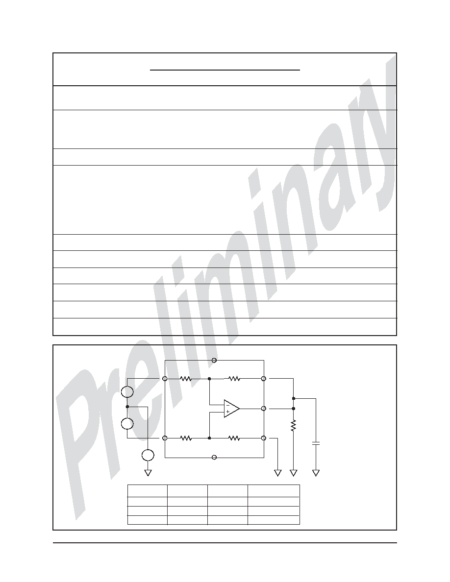
R
2
R
1
R
4
R
3
Sense
Vout
Ref
Vcc
Vee
V
CM
In+
In-
ΩU
diff
R
L
ΩU
diff
~
~
~
Gain
R = R
9 k
1
3
Ÿ
Ÿ
Ÿ
10.5 k
12 k
R = R
9 k
2
4
Ÿ
Ÿ
Ÿ
7.5 k
6 k
Part no.
b
a
C
L
THAT1240
THAT1243
THAT1246
0 dB
-3 dB
-6 dB
Figure 2. THAT1240 series test circuit

Application Notes
The THAT 1240, 1243, and 1246 are precision
differential amplifiers with gains of zero, -3 and -6 dB
respectively, and are primarily intended as balanced
line receivers for pro audio. However, their topology
lends itself to other applications as well.
Figures 3 and 4 show the THAT 1240 and
THAT 1246 configured as zero and -6 dB line receiv-
ers respectively. These devices can be used to retrofit
circuits currently using the SSM 2141, INA134,
SSM2143, or INA137.
While the THAT 1240 and
THAT 1246 are form, fit and functionally compatible
with their competitors' equivalent versions, their slew
rate and bandwidth are superior.
Like other amplifiers of this type, all of THAT
Corporation's line receivers can accept common
mode voltages that exceed the power supply rails.
Consider Figure
2. Assume that the circuit is con-
figured as shown, but with no differential excitation.
In+ and In- are shorted together, as are Vout and
Sense. Ref is tied to ground. a and b will be held at
the same voltage by feedback.
The maximum voltage allowed at the internal
node a is V
CC
minus 2V, while the minimum voltage is
V
EE
plus 2V. The voltage at a can be calculated
a
V
PK CM
=
-
+
[
]
R4
R3 R4
Isolating V
PK-CM
, we see that
V
a
PK CM
R
R
R
-
+
=
[
]
4
3
4
Thus, the maximum input in dBu would be
V
IN
dbu
Vcc
V
R
R
R
max
.
log
(
)
[
]
-
¥
=
È
Î
Í
Í
˘
˚
˙
˙
-
+
20
2
2
4
3
4
0775
With ±18V supplies, the THAT 1240 can tolerate
a maximum common mode input of 29.3 dBu. Un-
der the same conditions, the THAT1243 can tolerate
30.0 dBu and the THAT 1246 can tolerate 32.9 dBu.
These numbers are slightly higher than the datasheet
specifications, since they're calculated with a slightly
higher supply voltage. Also note that high levels of
common mode input compromise the maximum dif-
ferential mode signal that can be handled by these
ICs.
Figure 5 shows a THAT 1240 configured as a pre-
cision summing amplifier. This circuit uses both the
In+ and Ref pins as inputs. Refering to Figure 2, it
can be shown by superposition that the voltage at a
will be
a
In
R
R
R
R
R
R
R
=
+
+
+
+
(
) [
]
[
]
4
4
3
3
4
3
ef
THAT Corporation; 45 Sumner Street; Milford, Massachusetts 01757-1656; USA
Tel: +1 (508) 478-9200; Fax: +1 (508) 478-0990; Web: www.thatcorp.com
Page 4
Balanced Line Receiver ICs
Preliminary Information
Vout
6
In+
3
In-
2
U1
1240
Hi
Lo
Hi - Lo
Sense
Ref
1
5
Figure 3. Zero dB line receiver
Vout
6
In+
3
In-
2
U1
1246
Hi
Lo
( Hi - Lo ) * 0.5
Sense
Ref
1
5
Figure 4. -6 dB line receiver
Vout
6
In+
3
In-
2
U1
1240
In+
Ref
(In+)+ Ref
Sense
Ref
1
5
Figure 5. Precision summing circuit

Since R3=R4 in the THAT 1240, this equation
can be simplified to
a
In
R
=
+ +
(
)
ef
2
The output voltage would then be
Vout
a
R
R
= ¥ +
(
)
1
2
1
Since R2=R1, combining equations results in
Vout
In
R
=
+ +
(
)
ef
Figure 6 shows a convenient method of driving a
typical audio ADC with balanced inputs. This circuit
accepts
+24
dBu
in,
and
using
a
pair
of
THAT 1246s, the signal level between their respective
outputs is +24 dBu. An attenuator network brings
the signal down another 24 dB while attenuating the
noise of the line receivers as well.
The output noise of a THAT 1246 is -109 dBu,
and since there are two of them, the total noise level
going into the resistive pad will be -106 dBu.
The
pad reduces the noise level to -130 dBu at the input
to the ADC. The noise density resulting from the line
receivers will therefore be
THAT Corporation; 45 Sumner Street; Milford, Massachusetts 01757-1656; USA
Tel: +1 (508) 478-9200; Fax: +1 (508) 478-0990; Web: www.thatcorp.com
Rev. 04/29/02
Page 5
Preliminary Information
In Hi
In Lo
AIN- to ADC
AIN+ to ADC
R8
2k10
R9
249R
R19
2k10
C4
6n8
+24 dBu In
Vout
6
In+
3
In-
2
U1
THAT
1246
Vout
6
In+
3
In-
2
U2
3
2
1
U3A
4570
1/2 Vref of ADC
+24 dBu
Zero dBu Out
Ref
Sense
5
1
Ref
Sense
5
1
THAT
1246
Figure 6. Circuit for audio ADCs with balanced inputs
Vout
6
In+
3
In-
2
U1
1243
In Hi
In Lo
Out Hi
Out Lo
In
4
Gnd
3
Out-
1
Out+
8
U2
THAT1430
C1
100n
R1
1M0
R2
20k0
R4
5k1
R3
14k0
C2
22u
C3
22p
IN
1
8
OUT
U3
2180B
3
2
1
U4A
4570
VEE
VCC
VCC
VEE
Control Voltage
-3dB
+6dB
Vee
Cap2
Vcc
Cap1
6
7
2
5
GND
EC-
EC+
SYM
V-
V+
5
6
3
2
4
7
Sense
Ref
5
1
-3dB
Figure 7. Automated gain control of a balanced signal