 | –≠–ª–µ–∫—Ç—Ä–æ–Ω–Ω—ã–π –∫–æ–º–ø–æ–Ω–µ–Ω—Ç: THAT1430 | –°–∫–∞—á–∞—Ç—å:  PDF PDF  ZIP ZIP |
THAT Corporation; 45 Sumner Street; Milford, Massachusetts 01757-1656; USA
Tel: +1 (508) 478-9200; Fax: +1 (508) 478-0990; Web: www.thatcorp.com
THAT 1420, 1430
Description
The THAT 1420 and 1430 are a new genera-
tion of audio differential line drivers with im-
proved
performance
over
conventional
cross-coupled monolithic designs. Both models
exhibit low noise and distortion, high slew rate,
stability under difficult loads, wide output swing,
and have outputs which are short-circuit pro-
tected.
In addition both models incorporate patented
OutSmarts‘ technology, a dual feedback-loop de-
sign that prevents the excessive ground currents
typical of cross-coupled output stages (CCOS)
when clipping into single-ended loads
1
.
To overcome this problem, the THAT 1420
and 1430 use two individual negative-feedback
loops to separately control the differential output
voltage and common mode output currents, mak-
ing the design inherently more stable and less
sensitive to component tolerances than the CCOS.
Most importantly, the dual-feedback design pre-
vents the loss of common-mode feedback that
plagues the CCOS designs, avoiding the excessive
ground currents and overly-distorted output
waveform that can result when driving sin-
gle-ended loads.
Where minimum output offset voltage with
minimum parts count is desired, the THAT 1430
further improves over existing designs. In con-
ventional CCOS circuits, two relatively high-value
electrolytic capacitors are required to reduce the
offset voltage. By contrast, the THAT 1430 topol-
ogy requires only a resistor and a single film or
ceramic capacitor to achieve the same effect at
lower parts count and price.
T H A T
C o r p o r a t i o n
OutSmarts‰ Balanced Line Drivers
FEATURES
∑
OutSmarts‘ technology tames
clipping behavior into single-ended
loads
∑
Pin-compatible with SSM2142
∑
Balanced, floating output delivers
transformer-like behavior
∑
Stable when driving long cables
and capacitive loads
∑
THAT 1430 delivers low output
offset voltage using single capacitor
APPLICATIONS
∑
Differential Line Driver
∑
Audio Mix Consoles
∑
Distribution Amplifiers
∑
Audio Equalizers
∑
Dynamic Range Processors
∑
Digital Effects Processors
∑
Telecommunications Systems
∑
Instrumentation
∑
Hi-Fi Equipment
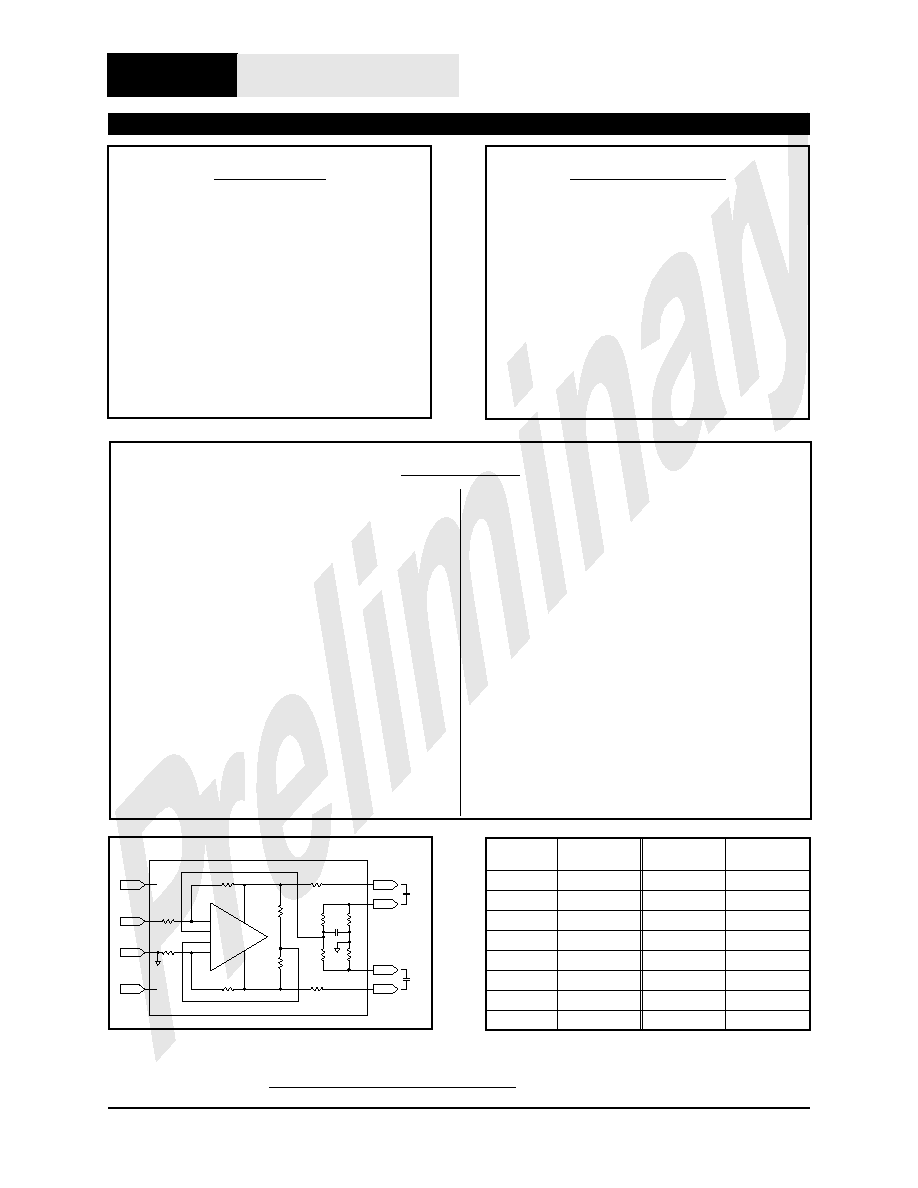
Din+
Cin+
Cin-
Din-
Out-
Sens+
Out+
Sens-
Vcc
In+
Vee
Gnd
Dout-
Dout+
10k
10k
50
5k
5k
10k
10k
10k
10k
20k
20k
10p
50
THAT 1420
C
EXT
C
EXT
D
C
A
A
&
Figure 1. THAT 1420 Equivalent Circuit Diagram
1. See Gary Hebert's paper, An Improved Balanced, Floating Output Driver IC, presented at the 108th AES Convention, Feb. 2000
DIP Pin
Number
SO Pin
Number
1420 Pin
Name
1430 Pin
Name
1
3
Out-
Out-
2
4
Sens-
Cap2
3
5
Gnd
Gnd
4
6
In
In
5
11
Vee
Vee
6
12
Vcc
Vcc
7
13
Sens+
Cap1
8
14
Out+
Out+
Table 1. THAT 1420/1430 pin assignments

THAT Corporation; 45 Sumner Street; Milford, Massachusetts 01757-1656; USA
Tel: +1 (508) 478-9200; Fax: +1 (508) 478-0990; Web: www.thatcorp.com
Page 2
THAT1420/1430 Balanced Line Driver
Preliminary Information
Absolute Maximum Ratings (T
A
= 25∞C)
Positive Supply Voltage (Vcc)
+18 V
Operating Temperature Range (T
OP
)
-40 to +85∞C
Negative Supply Voltage (Vee)
-18 V
Storage Temperature (T
ST
)
-40 to +150∞C
Output Short Circuit Duration
Continuous
Junction Temperature (T
J
)
150∞C
Power Dissipation (P
D
)
TBD mW
Lead Temperature (T
LEAD
)(Soldering 60 sec)
300∞C
SPECIFICATIONS
2
2. All specifications are subject to change without notice.
3. All measurements taken with V
S
=±18, T=25∞C, unless otherwise noted
Electrical Characteristics
3
Parameter
Symbol
Conditions
Min.
Typ.
Max.
Units
Input Impedance
Z
IN
4
5
kW
Gain
G1
R
L
=600W
Balanced
4.35
4.65
4.95
dB
Single Ended
4.4
4.6
4.8
dB
Gain
G2
R
L
=100kW
Balanced
5.8
6
6.2
dB
Single Ended
5.8
6
6.2
dB
DC Power Supply
Rejection Ratio
PSRR
±4V to ±18V
80
105
dB
Output Common-Mode
Rejection Ratio
OCMRR
f=1kHz, BBC Method
50
68
dB
Output Signal Balance Ratio
SBR
f=1kHz, BBC Method
28
40
dB
THD+N (Balanced)
THD+N
1
20Hz-20kHz
0.001
%
1kHz
0.0005
%
THD+N (Single Ended)
THD+N
2
V
O
=10 V
RMS
, R
L
=600W, 20Hz-20kHz
0.0018
%
Output Noise
SNR
Bal. Mode, 20 kHz BW
-104
dBV
Headroom
HR
0.1% THD+N
25
dBV
Slew Rate
SR
16
V/mS
Output Common Mode
Voltage Offset
V
OCM
R
L
=600W, w/o Sense capacitors
-300
±60
300
mV
THAT1420
V
OCM
R
L
=600W, w/ Sense capacitors
-6
±4
6
mV
Output Common Mode
Voltage Offset
V
OCM
R
L
=600W, w/o Sense capacitor
-400
±80
400
mV
THAT1430
V
OCM
R
L
=600W, w/ Sense capacitor
-20
±10
20
mV
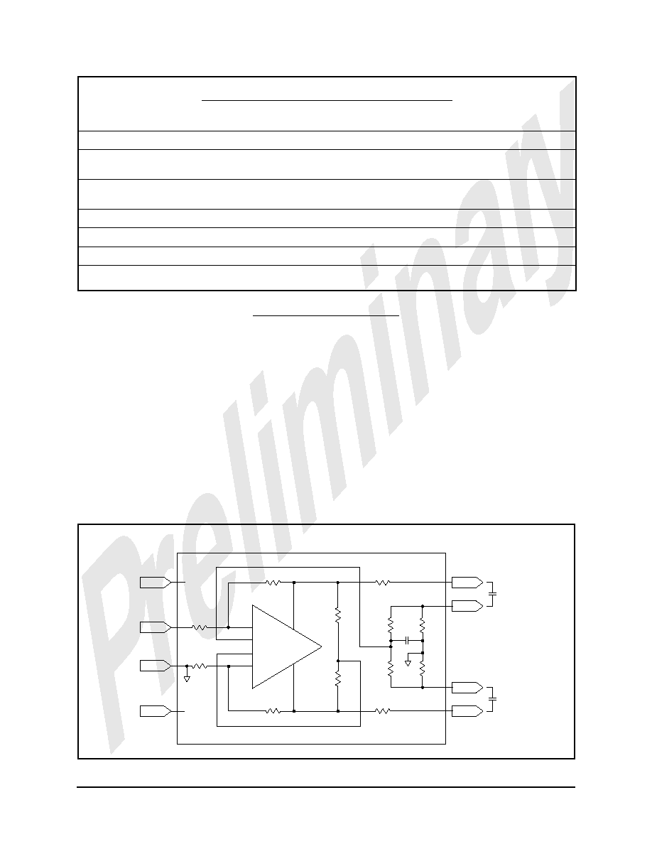
Theory of Operation
OutSmarts‘ technology
The THAT 1420 and 1430 are similar devices,
both employing the OutSmarts topology, a variation
of circuitry originally developed at Audio Toys, Inc.
OutSmarts topology employs two negative-feedback
loops -- one to control the differential signal, and a
separate loop to control the common mode output
levels.
Figures 2 and 3 show the gain core common to
both the THAT 1420 and 1430. The gain core is a
single amplifier that includes two differential input
pairs, C
in+/-
and D
in+/-
, and complementary outputs,
V
out+
and V
out-,
related to each other by two gain ex-
pressions, A
D
(s) and A
C
(s). The first pair of differen-
tial inputs, D
in+/-
, are connected to the differential
feedback network between the outputs and the input
signal. The second differential input pair, C
in+/-
, is
connected to a bridge circuit which generates an er-
ror signal that is used to servo the common-mode be-
havior of the outputs. The loop equations are then,
(
)
D
D
D
A D
D
OUT
OUT
OUT
D
IN
IN
+
-
+
-
-
=
=
-
D
where A
D
is the differential open-loop gain, and
(
)
D
D
D
A C
C
OUT
OUT
OUT
C
IN
IN
+
-
+
-
+
=
=
-
Â
where A
C
is the common-mode open-loop gain.
THAT Corporation; 45 Sumner Street; Milford, Massachusetts 01757-1656; USA
Tel: +1 (508) 478-9200; Fax: +1 (508) 478-0990; Web: www.thatcorp.com
Rev. 4/24/01
Page 3
Preliminary Information
Electrical Characteristics (cont'd.)
Parameter
Symbol
Conditions
Min.
Typ.
Max.
Units
Differential Output Offset
V
OOD
R
L
=600W
-10
±4
10
mV
Differential Output
Voltage Swing,Pos
V
IN
= ±18V
V
CC
-2
V
Differential Output
Voltage Swing,Neg
V
IN
= ±18V
V
EE
+2
V
Output Impedance
Z
O
40
50
60
W
Quiescent Supply Current
I
S
Unloaded, V
IN
= 0
4
5.2
mA
Short Circuit Output Current
I
SC
60
70
mA
Voltage Supply Range
±4
±18
V
Din+
Cin+
Cin-
Din-
Out-
Sens+
Out+
Sens-
Vcc
In+
Vee
Gnd
Dout-
Dout+
10k
10k
50
5k
5k
10k
10k
10k
10k
20k
20k
10p
50
THAT 1420
C
EXT
C
EXT
D
C
A
A
&
Figure 2. THAT 1420 Equivalent Circuit Diagram
These equations can be solved much like standard
op-amp loop equations, and for the differential case,
we can see that (using superposition) resistor feed-
back results in
D
D
In
IN
OUT
+
-
+
=
+
(
)
1
3
2
3
and
D
D
IN
OUT
-
+
=
1
3
Substituting and simplifying into the equation that
defines differential operation yields
D
D
D
A
In
OUT
D
D
OUT
=
+
-
+
(
)
3
2
3
Dividing through by A
D
(assuming that A
D
>> 3) and
simplifying yields
( )
D D
In
OUT
=
+
2
as one would expect for a +6dB line driver.
The derivation for the common mode equation is
more complicated
1
in that it is dependent on the at-
tached load, and in any event doesn't yield much
insight into the device's operation.
In op-amp analysis or in the above derivation, the
combination of negative feedback and high open-loop
gain results in the open-loop gain "dropping out" of
the equation, and the differential inputs being forced
to the same potential. If we start with that assump-
tion, we can intuitively discern the operation of the
common-mode feedback loop as follows:
Referring again to Figures 2 and 3, the com-
mon-mode input actually senses the sum of the IC's
output currents by way of two 50 ohm resistors and
the bridge network (the 10pF capacitor simply limits
the maximum frequency at which this action occurs).
The resulting error signal is amplified and then
summed into both outputs, with the net effect being
to force the sum of the currents to be zero, and thus
the common mode output current to zero. Since this
is negative feedback, the common-mode loop can
raise the effective output impedance at audio fre-
quencies without the side effects of circuits that use
positive feedback to implement this function.
THAT Corporation; 45 Sumner Street; Milford, Massachusetts 01757-1656; USA
Tel: +1 (508) 478-9200; Fax: +1 (508) 478-0990; Web: www.thatcorp.com
Page 4
THAT1420/1430 Balanced Line Driver
Preliminary Information
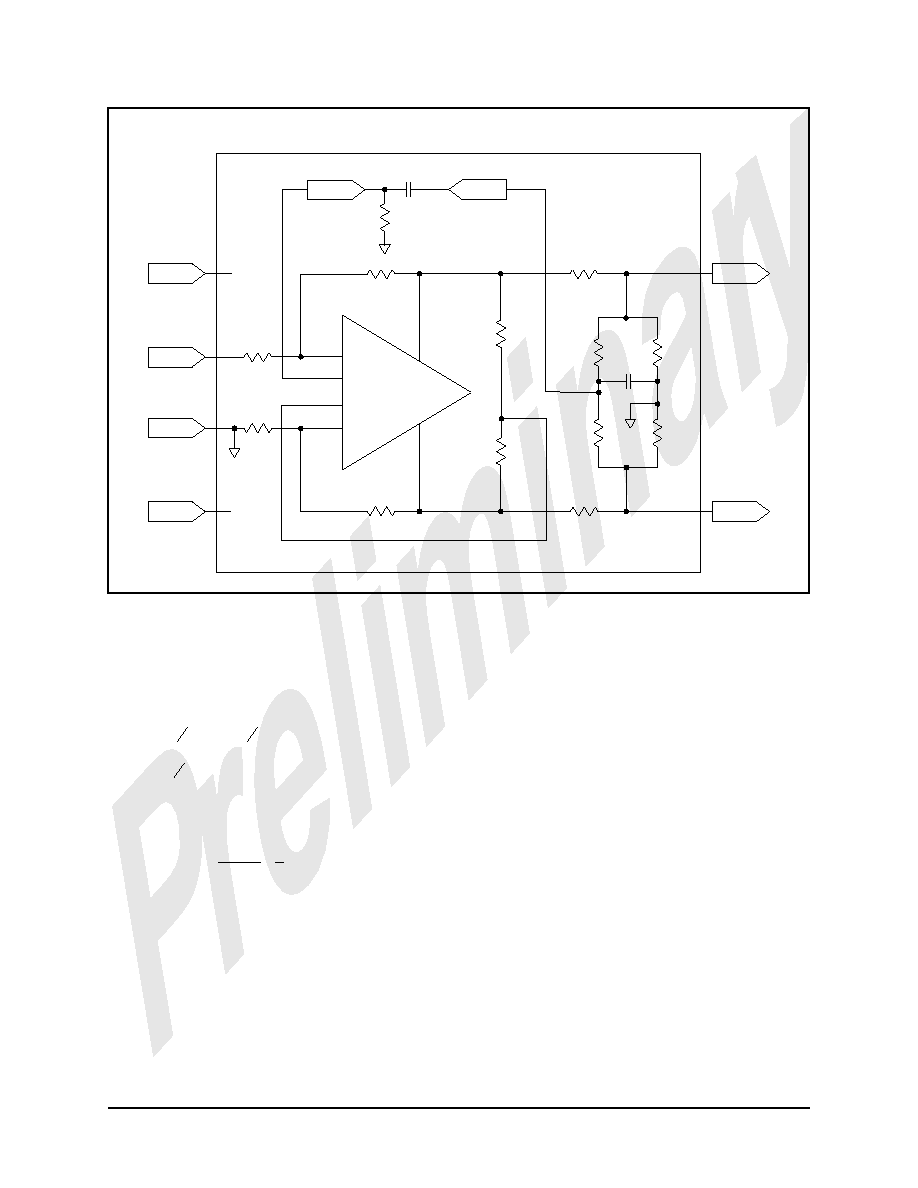
Out-
Cap1
Cap2
Out+
Vcc
In+
Vee
Gnd
10k
10k
50
5k
5k
10k
10k
10k
10k
7k
7k
10p
50
THAT 1430
C
EXT
R
EXT
Din+
Cin+
Cin-
Din-
Dout-
Dout+
D
C
A
A
&
Figure 3. THAT 1430 Equivalent Circuit Diagram
Applications
Circuit
implementations
using
the
THAT
1420/1430 are relatively straightforward. A quiet,
solid ground reference, stiff voltage supplies, and ad-
equate supply bypassing are all that is required to
achieve excellent performance out of both ICs. Both
devices are stable into any capacitive load, and the
maximum capacitance is limited only by slew rate
and frequency response considerations.
For the purposes of the frequency response calcu-
lation, the line driver's 50W sense resistors can be
lumped into a single 100W resistor. The correct ca-
ble capacitance to use is the sum of the
inter-conductor capacitance and the two conduc-
tor-to-shield capacitances. Unfortunately, some man-
ufacturers
only
specify
the
inter-conductor
capacitance and the capacitance of one conductor to
the other while connected to the shield, and some ex-
traction may be required.
As an example, one manufacturer supplies a
shielded, twisted pair with 30pF/ft of inter-conductor
capacitance and 25pF/ft of conductor to shield capac-
itance. The corner frequency of the THAT 1420/1430
driving 500 ft of this cable will be
f
kHz
C
pF
ft
pF
ft
pF
ft
=
ª
¥ ¥
¥
+
+
1
2
100
500 30
25
25
40
p
W
(
)
One must also consider the slew rate limitations
posed by excessive cable and other capacitances. We
know that
i C
dV
dt
=
and that
dV
dt
Peak
V
f
=
¥
¥
2p
Rane Corporation has published a document titled
RaneNote 126
4
, which specifies some of the require-
ments for a balanced line driver, including a)
stablility into reactive loads, b) output voltage swing
of at least ±11 volts peak (+20dBu), and c) reliabil-
ity. This document also suggests a reasonable rule
by which to calculate the output current require-
ments at 20kHz. The author concludes that the ac-
THAT Corporation; 45 Sumner Street; Milford, Massachusetts 01757-1656; USA
Tel: +1 (508) 478-9200; Fax: +1 (508) 478-0990; Web: www.thatcorp.com
Rev. 4/24/01
Page 5
Preliminary Information
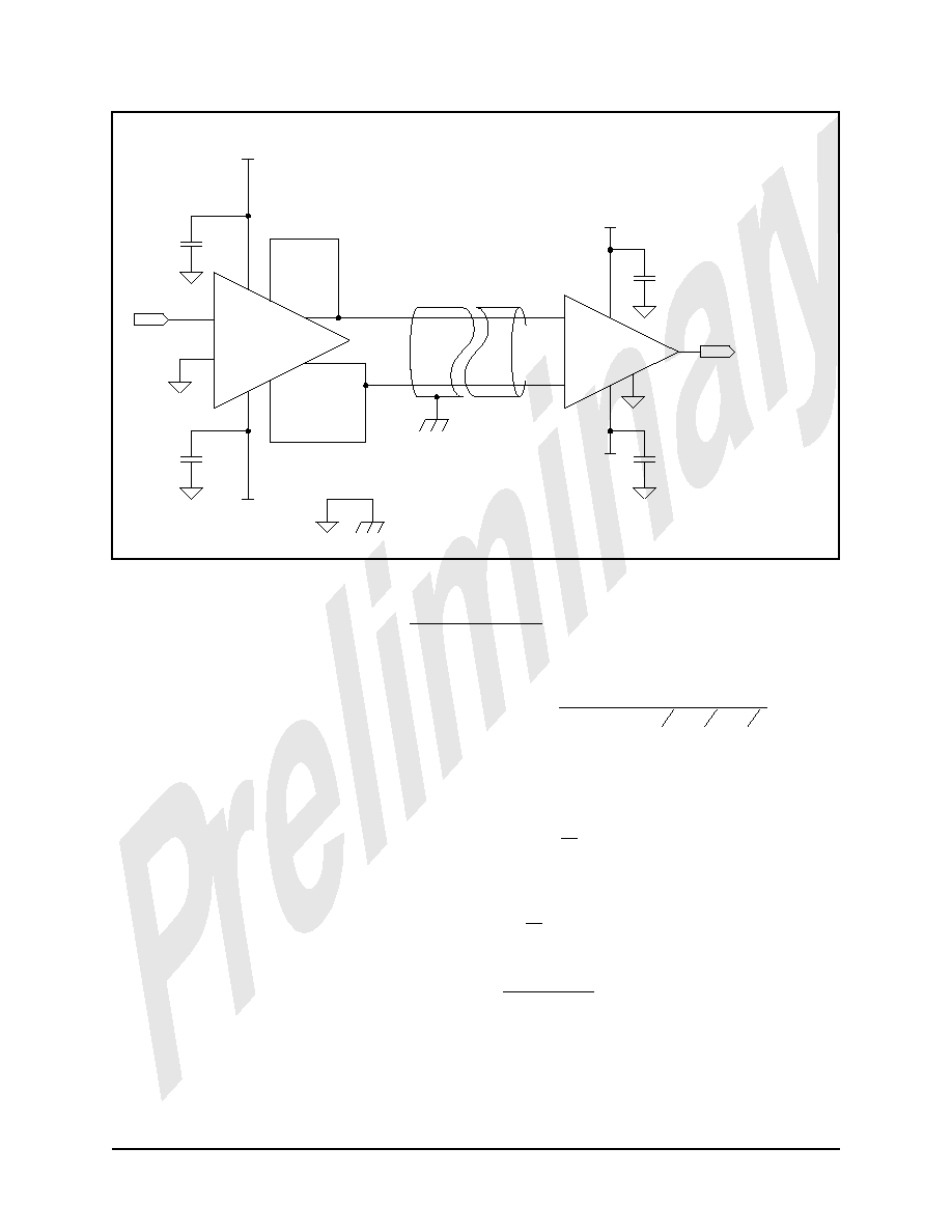
In
4
Gnd
3
5
2
Out-
1
Out+
8
7
6
U1
THAT1420
In
VCC
VEE
1
In-
2
In+
3
4
7
Out
6
U2
THAT1243 or equiv.
VEE
VCC
Out
C4
100n
C5
100n
C6
100n
C7
100n
Vcc
Sens+
Vee
Sens-
Vcc
Vee
Ref
Figure 4. Basic THAT 1420 applications circuit
4. Copyright „ 1991 Rane Corporation