THAT Corporation; 734 Forest Street; Marlborough, Massachusetts 01752; USA
Tel: (508) 229-2500; Fax: (508) 229-2590
-
+
INPUT
2
1
7
6
5
4
3
(-50mV/dB)
6k04
7k32
100p
INPUT
CONTROL
SIGNAL
OUT
IN
-15V
-15V
100k
+15V
+15V
5534
22uf
50k
SYM
OUTPUT
SIGNAL
V+
V-
Ec
SYM
GND
202XT
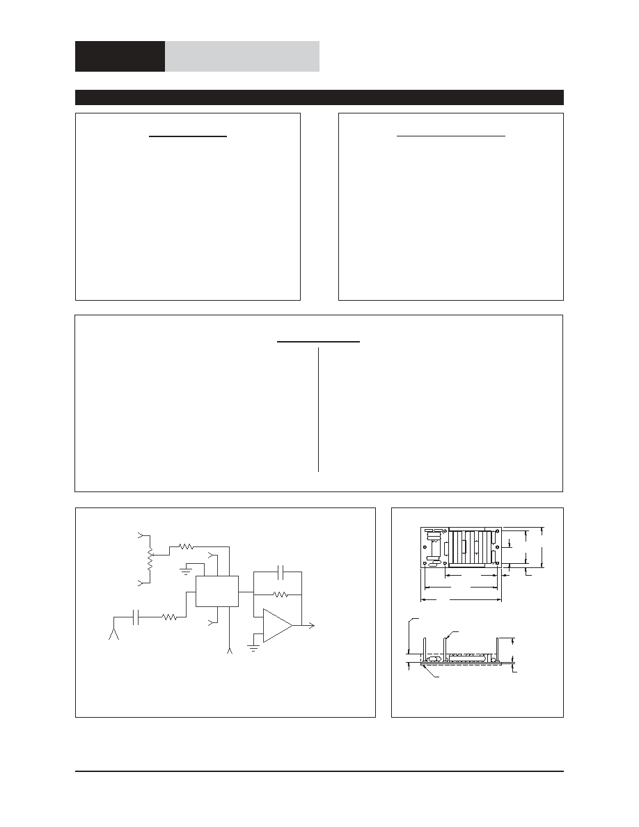
Figure 1. 202XT, 202XTC Typical Application Circuit
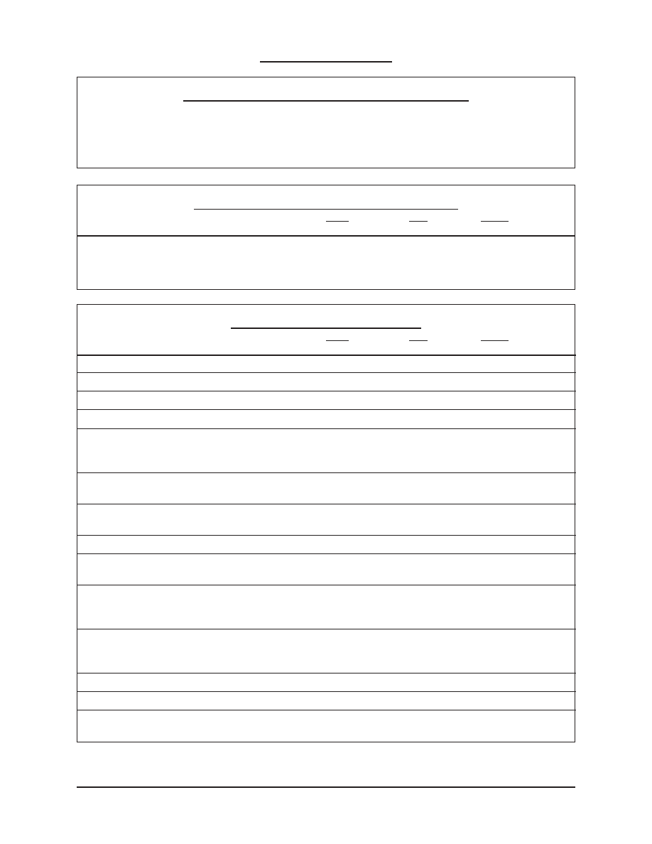
2.00
1.800
1.300
.10
.400
.10
1.00
.800
(25.4)
(20.32)
(10.16)
(2.54)
(2.54)
(33.02)
(45.72)
(50.8)
BOTTOM VIEW
.062
.60
.040 MAX (1.02 MAX.)
LEADS AND SOLDER
(15.24)
(1.57)
.040 DIA.
(1.02 DIA.)
7 PLACES
.250 MAX.
COMPONENT
HEIGHT
(6.35 MAX.)
CLEARANCE FOR
SIDE VIEW
U9
U8
U7
U6
U5
U4
U3
U2
U1
RP1
RP2
CO
RP
TH
A
T
R8
R7
R6
R5
R4
R3
R2
R1
C4
C3
C2
C1
DIMENSIONS ARE IN INCHES
RP1
C3
AND MILLIMETERS (mm)
1
2
3
4
5
6
7
Figure 2. 202XT, 202R, 202XTC Physical
Outline
FEATURES
�
Wide Dynamic Range: >124 dB
�
Wide Gain Range: > 130 dB
�
Logarithmic Gain Control
�
Very Low Distortion: (0.003%
@0 dB gain, 0.02% @20dB gain)
�
Temperature Compensated
(202XTC)
�
Package Compatible with dbx 202
APPLICATIONS
�
Faders
�
Console Automation
�
Panners
�
Compressors
�
Expanders
�
Filters
�
Oscillators
Description
The THAT 202XT, 202XTC and 202R2 modu-
lar voltage-controlled amplifiers (VCAs) are ex-
tremely high performance current-in/current-out
devices with negative-sense control ports. Intended
for the most demanding of applications, these parts
require almost no external support circuitry and
are packaged on small, 1" X 2" circuit boards. Their
pin configurations are identical to that of the origi-
nal dbx 202 VCA, as well as later dbx models 202C,
202X, 202XL and 2001. The 202XTC has a control
constant of �20dB/Volt, and is internally tempera-
ture compensated for very low thermal drift. The
202XTC is recommended for all new designs. The
202XT is intended to replace a dbx 202C, 202X or
202XL in designs where control-voltage tempera-
ture compensation was provided externally. Like
the 202C, -X and -XL, the 202XT has a control con-
stant of �20dB/Volt, with a predictable +0.33%/�C
temperature drift. The 202R is intended to replace
the original dbx 202. The 202R matches the dbx
202's control sensitivity of �6mV/dB and its predict-
able +0.33%/�C temperature drift
dbx is a registered trademark of Carillon Electronics Corporation
T H A T
C o r p o r a t i o n
THAT
202XT, 202XTC, 202R
Modular Voltage-Controlled
Amplifiers
THAT Corporation; 734 Forest Street; Marlborough, Massachusetts 01752; USA
Tel: (508) 229-2500; Fax: (508) 229-2590
Absolute -Maximum Ratings (T
A
= 25�C)
Positive Supply Voltage (V
CC
)
+18 V
Negative Supply Voltage (V
EE
)
-18 V
Supply Current (I
CC
)
40 mA
Power Dissipation (P
D
)
1.5 W
Operating Temperature Range (T
OP
)
-20 to +75�C
Storage Temperature Range (T
ST
)
-40 to +125�C
Recommended Operating Conditions
202XT
202R
202XTC
Parameter
Symbol
Conditions
Min
Typ
Max
Min
Typ
Max
Min
Typ
Max
Units
Positive Supply Voltage
V
CC
+12
+15
+16
12
+15
+16
+12
+15
+16
V
Negative Supply Voltage
V
EE
12
-15
-16
-12
-15
-16
-12
-15
-16
V
Signal Current
V
CC
=-V
EE
=15 V
--
1.4
6.0
--
1.4
6.0
--
1.4
6.0
mA
Electrical Characteristics
2
202XT
202R
202XTC
Parameter
Symbol
Conditions
Min
Typ
Max
Min
Typ
Max
Min
Typ
Max
Units
Supply Current
I
CC
No Signal
--
26
33
--
26
33
--
26
33
mA
Input Impedance
R
IN
1.18
1.25
1.32
1.18
1.25
1.32
1.18
1.25
1.32
k
W
Equiv. Input Bias Current
I
B
No Signal
--
40
64
--
40
64
--
40
64
nA
Input Offset Voltage
V
OFF(IN)
No Signal
--
+10
--
--
+10
--
--
+10
--
mV
Output Offset Voltage
V
OFF(OUT)
R
out
=7.32 k
W
-100 dB < gain< 0 dB
--
1
2
--
1
2
--
1
2
mV
+20 dB gain
--
5
10
--
5
10
--
5
10
mV
Gain-Control Constant
dB gain/E
C
T
A
=27
�C
-100 dB< gain <+40 dB
19.3
20
20.7
161.0 166.7 172.6
19.3
20
20.7
dB/V
Gain-control TempCo
DGain/DT
A
0
�C<T
A
<70
�C
E
C
constant
--
-0.33
--
--
-0.33
--
-0.04
0.0
+0.04
%/
�C
Gain-Control Linearity
-60 to +40 dB gain
--
0.5
2
--
0.5
2
--
0.5
2
%
Off Isolation
E
C
= -6V
110
115
--
--
--
--
110
115
dB
E
C
= -.72V
--
--
--
110
115
--
dB
Output Noise
e
n(OUT)
20Hz-20kHz,R
out
= 7.32k
W
0 dB gain
--
-98
-95
--
-98
-95
--
-98
-95
dBV
+20 dB gain
--
-85
-82
--
-85
-82
--
-85
-82
dBV
Total Harmonic Distortion
THD
I
IN
+I
OUT
=700 mA,1kHz
0 dB gain
--
0.003 0.01
--
0.003 0.01
--
0.003 0.01
%
�20 dB gain
--
0.02
0.05
--
0.02
0.05
--
0.02
0.05
%
Symmetry Control Voltage
V
SYM
A
V
=0dB, THD<0.01%
-8
0
+8
-8
0
+8
-8
0
+8
mV
Symmetry Port Impedance
R
SYM
T
A
= 27�C
48.4
51
53.6
48.4
51
53.6
48.4
51
53.6
W
Control Port Impedance
Rc
Ta = 27�C
813
822
831
200
203
206
798
842
885
W
1. All specifications subject to change without notice.
2. Unless otherwise noted, T
A
=25�C, V
CC
= +15V, V
EE
= -15V. Test circuit is as shown in Figure 1.
SPECIFICATIONS
1
Rev. 09/28/93