 | –≠–ª–µ–∫—Ç—Ä–æ–Ω–Ω—ã–π –∫–æ–º–ø–æ–Ω–µ–Ω—Ç: THAT2180 | –°–∫–∞—á–∞—Ç—å:  PDF PDF  ZIP ZIP |
THAT Corporation; 45 Sumner Street; Milford, Massachusetts 01757-1656; USA
Tel: +1 508 478 9200; Fax: +1 508 478 0990; Web: www.thatcorp.com
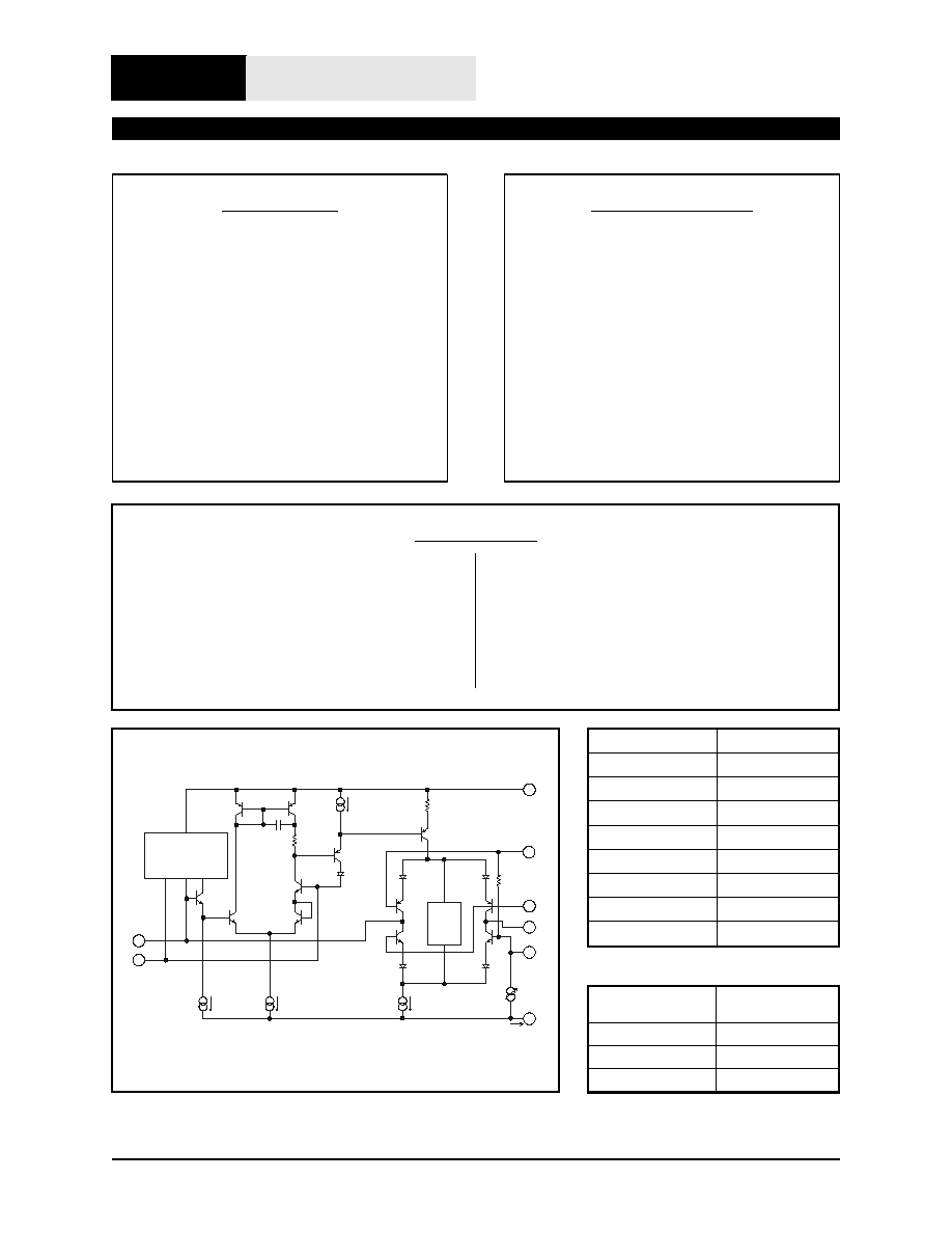
BIAS CURRENT
COMPENSATION
Vbe
MULTI-
PLIER
Output
Sym
Iset
V-
Vcc
Ec+
Ec-
Iadj
Input
Gnd
7
2
3
8
4
5
1
6
2k
25
Figure 1. 2180 Series Equivalent Circuit Diagram
Pin Name
SIP Pin
Input
1
Ec+
2
Ec≠
3
Sym
4
V≠
5
Gnd
6
V+
7
Output
8
Table 1. 2180 Series Pin Assignments
FEATURES
∑
Wide Dynamic Range: >120 dB
∑
Wide Gain Range: >130 dB
∑
Exponential (dB) Gain Control
∑
Low Distortion: < 0.01 % (2180A)
∑
Wide Gain-Bandwidth: 20 MHz
∑
Dual Gain-Control Ports (pos/neg)
∑
Pin-Compatible with 2150-Series
APPLICATIONS
∑
Faders
∑
Panners
∑
Compressors
∑
Expanders
∑
Equalizers
∑
Filters
∑
Oscillators
∑
Automation System
Description
THAT 2180 Series integrated-circuit voltage con-
trolled amplifiers (VCAs) are very high-performance
current-in/current-out
devices
with
two
oppos-
ing-polarity, voltage-sensitive control ports. They offer
wide-range exponential control of gain and attenuation
with low signal distortion. The parts are trimmed at
wafer stage for low THD and control-voltage
feedthrough without further adjustment.
The VCA design takes advantage of a fully comple-
mentary dielectric isolation process which offers
closely matched NPN/PNP pairs, to deliver discrete
performance at IC prices. The parts are available in
three grades, selected for factory trimmed distortion,
alowing the user to optimize cost vs. performance. The
2180 Series is available in an 8-pin single-in-line (SIP)
package.
Max THD @1 V,
1 kHz, 0 dB
Plastic
SIP
0.01%
2180LA
0.02%
2180LB
0.05%
2180LC
Table 2. Ordering Information
T H A T
C o r p o r a t i o n
THAT 2180A, 2180B, 2180C
Pre-Trimmed IC
Voltage Controlled Amplifiers

THAT Corporation; 45 Sumner Street; Milford, Massachusetts 01757-1656; USA
Tel: +1 508 478 9200; Fax: +1 508 478 0990; Web: www.thatcorp.com
Page 2
THAT2180 Series IC VCAs
SPECIFICATIONS
1
Absolute-Maximum Ratings (T
A
= 25∞C)
Positive Supply Voltage (V
CC
)
+20 V
Negative Supply Voltage (V
EE
)
-20 V
Supply Current (I
CC
)
10 mA
Max DE
C
E
C+
- (E
C-
)
± 1V
Power Dissipation (P
D
) (T
A
= 75∞C)
330 mW
Operating Temperature Range (T
OP
)
0 to +70∞C
Storage Temperature Range (T
ST
)
-40 to +125∞C
Recommended Operating Conditions
2180A
2180B
2180C
Parameter
Symbol
Conditions
Min Typ
Max
Min Typ
Max
Min Typ
Max Units
Positive Supply Voltage V
CC
+4 +15 +18
+4 +15 +18
+4 +15 +18
V
Negative Supply Voltage V
EE
-4
-15 -18
-4
-15 -18
-4
-15 -18
V
Bias Current
I
SET
V
CC
- V
EE
= 30 V
1
2.4
5
1
2.4
5
1
2.4
5
mA
Signal Current
I
IN
+I
OUT
I
SET
= 2.4mA
-- 0.35 1.5
-- 0.35 1.5
-- 0.35 1.5
mA
rms
Electrical Characteristics≤
2180A
2180B
2180C
Parameter
Symbol
Conditions
Min Typ
Max
Min Typ
Max
Min Typ
Max Units
Supply Current
I
CC
No Signal
--
2.4
4
--
2.4
4
--
2.4
4
mA
Equiv. Input Bias Current I
B
No Signal
--
2
10
--
2
12
--
2
15
nA
Input Offset Voltage
V
OFF(IN)
No Signal
--
±5
--
--
±5
--
--
±5
--
mV
Output Offset Voltage V
OFF(OUT)
R
out
= 20 kW
0 dB gain
--
0.5
1
--
1
2
--
1.5
3
mV
+15 dB gain
--
1
3
--
1.5
4
--
3
10
mV
+30 dB gain
--
3
12
--
5
15
--
9
30
mV
Gain Cell Idling Current I
IDLE
--
20
--
--
20
--
--
20
--
mA
Gain-Control Constant
T
A
=25∞C (T
CHIP
@35∞C)
-60 dB < gain < +40 dB
E
C+
/Gain (dB)
Pin 2 (Fig. 14)
6.0
6.1
6.2
6.0
6.1
6.2
6.0
6.1
6.2
mV/dB
E
C-
/Gain (dB)
Pin 3
-6.2 -6.1 -6.0
-6.2 -6.1 -6.0
-6.2 -6.1 -6.0 mV/dB
Gain-Control TempCo DE
C
/ DT
CHIP
Ref T
CHIP
= 27∞C
-- +0.33 --
-- +0.33 --
-- +0.33 --
%/∞C
Gain-Control Linearity
-60 to +40 dB gain
--
0.5
2
--
0.5
2
--
0.5
2
%
1 kHz Off Isolation
E
C+
= -360 mV, E
C-
= +360 mV 110 115
--
110 115
110 115
--
dB
Output Noise
e
n(OUT)
20 Hz ~ 20 kHz
R
out
= 20kW
0 dB gain
--
-98 -97
--
-98 -96
--
-98 -95
dBV
+15 dB gain
--
-88 -86
--
-88 -85
--
-88 -84
dBV
Voltage at V-
V
V-
No Signal
-3.1 -2.85 -2.6
-3.1 -2.85 -2.5
-3.1 -2.85 -2.6
V
1. All specifications subject to change without notice.
2. Unless otherwise noted, T
A
=25∞C, V
CC
= +15V, V
EE
= ≠15V. Test circuit is as shown in Figure 2.
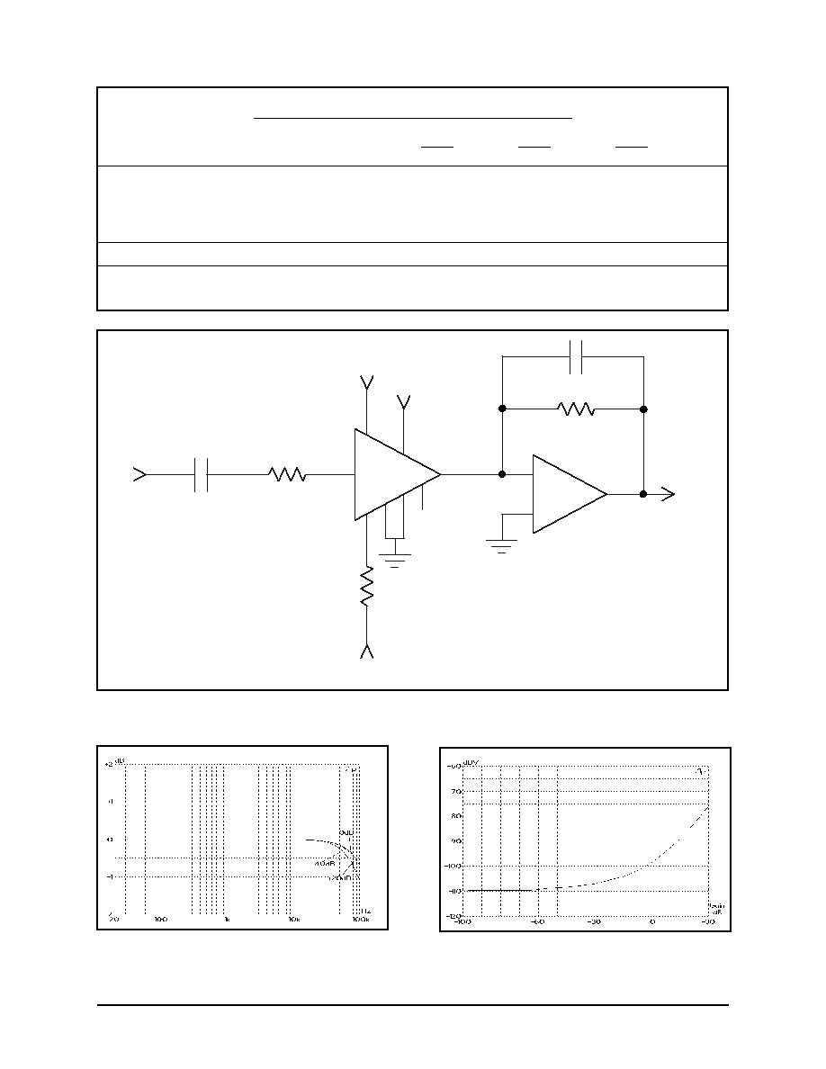
THAT Corporation; 45 Sumner Street; Milford, Massachusetts 01757-1656; USA
Tel: +1 508 478 9200; Fax: +1 508 478 0990; Web: www.thatcorp.com
600029 Rev 01
Page 3
Electrical Characteristics (Cont'd.)
2180A
2180B
2180C
Parameter
Symbol
Conditions
Min Typ
Max
Min Typ
Max
Min Typ
Max Units
Total Harmonic Distortion
THD
1 kHz, No External Trim
V
IN
= 0 dBV, 0 dB gain
-- 0.005 0.010
-- 0.010 0.020
-- 0.030 0.050
%
V
IN
= +10 dBV, -15 dB gain -- 0.020 0.030
-- 0.030 0.040
-- 0.040 0.070
%
V
IN
= -5 dBV, +15 dB gain
-- 0.020 0.030
-- 0.030 0.040
-- 0.040 0.070
%
Slew Rate
R
in
= R
out
= 20 kW
--
12
--
--
12
--
--
12
--
V/ms
Gain at 0 V Control Voltage
E
C-
= 0 mV
-0.1 0.0
+0.1 -0.15 0.0 +0.15 -0.2 0.0
+0.2
dB
Figure 3. 2180 Series Frequency Response Vs. Gain
Figure 4. 2180 Series Noise (20kHz NBW) Vs. Gain
Vcc
Ec-
IN
10u
20k
5.1k
Vee
OUT
22p
20k
OUT
OP275
7
3
8
4
2
6
5
1
V+
-IN
Ec-
Ec+
SYM
GND
V-
2180
Series
VCA
Power Supplies
Vcc = +15 V
Vee = -15 V
-
+
NC
Figure 2. Typical Application Circuit
THAT Corporation; 45 Sumner Street; Milford, Massachusetts 01757-1656; USA
Tel: +1 508 478 9200; Fax: +1 508 478 0990; Web: www.thatcorp.com
Theory of Operation
3
The THAT 2180 Series VCAs are designed for high
performance in audio-frequency applications requiring
exponential gain control, low distortion, wide dynamic
range and low control-voltage feedthrough. These parts
control gain by converting an input current signal to a
bipolar logged voltage, adding a dc control voltage, and
re-converting the summed voltage back to a current
through a bipolar antilog circuit.
Figure 5 presents a considerably simplified internal
circuit diagram of the IC. The ac input signal current
flows in pin1, the input pin. An internal operational
transconductance amplifier (OTA) works to maintain
pin 1 at a virtual ground potential by driving the emitters
of Q1 and (through the Voltage Bias Generator) Q3.
Q3/D3 and Q1/D1 act to log the input current, producing
a voltage, V3, which represents the bipolar logarithm of
the input current. (The voltage at the junction of D1 and
D2 is the same as V3, but shifted by four forward V
be
drops.)
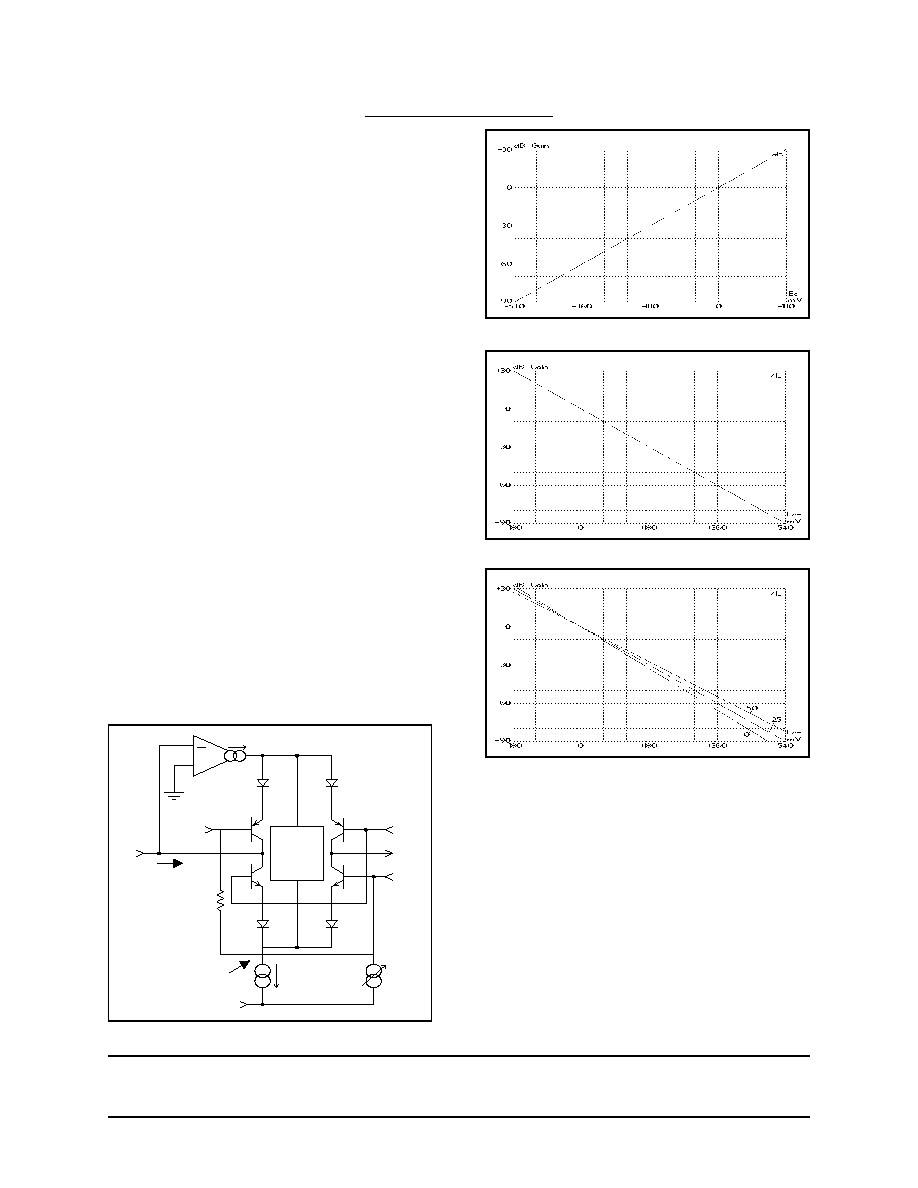
Gain Control
Since pin 8, the output, is usually connected to a vir-
tual ground, Q2/D2 and Q4/D4 take the bipolar antilog
of V3, creating an output current which is a precise rep-
lica of the input current. If pin 2 (Ec+) and pin 3 (Ec-)
are held at ground, the output current will equal the in-
put current. For pin 2 positive or pin 3 negative, the out-
put current will be scaled larger than the input current.
For pin 2 negative or pin 3 positive, the output current is
scaled smaller than the input.
The scale factor between the output and input cur-
rents is the gain of the VCA. Either pin 2 (Ec+) or pin 3
(Ec-), or both, may be used to control gain. Gain is expo-
nentially proportional to the voltage at pin 2, and expo-
nentially proportional to the negative of the voltage at
pin 3. Therefore, pin 2 (Ec+) is the positive control port,
while pin 3 (Ec-) is the negative control port. Because of
the exponential characteristic, the control voltage sets
gain linearly in decibels. Figure 6 shows the decibel cur-
rent gain of a 2180 versus the voltage at Ec+, while Fig-
ure 7 shows gain versus the Ec-.
Temperature Effects
The logging and antilogging in the VCA depends on
the logarithmic relationship between voltage and current
in a semiconductor junction (in particular, between a
transistor's V
be
and I
c
). As is well known, this relation-
ship is temperature dependent. Therefore, the gain of
any log-antilog VCA depends on its temperature.
Page 4
THAT2180 Series IC VCAs
3. For more details about the internal workings of the 2180 Series of VCAs, see An Improved Monolithic Volt-
age-Controlled Amplifier, by Gary K. Hebert (Vice-President, Engineering, for THAT Corporation), presented at the 99th
convention of the Audio Engineering Society, New York, Preprint number 4055.
Figure 6. Gain vs. Control Voltage (E
C+
, Pin 2) at 25∞C
Figure 7. Gain vs. Control Voltage (Ec-, Pin 3) at 25∞C
Figure 8. Gain vs. Control Voltage (Ec-) with Temp (∞C)
D1
IN
OUT
SYM
Ec-
D4
D3
Ec+
25
V-
+
Voltage
Bias
Generator
V
3
I
IN
Q1
Q4
Q3
Q2
Icell
Iadj
5
4
8
3
1
2
D2
Figure 5. Simplified Internal Circuit Diagram

Figure 8 shows the effect of temperature on the nega-
tive control port. (The positive control port behaves in the
same manner.) Note that the gain at Ec = 0 V is 0 dB, re-
gardless of temperature. Changing temperature changes
the scale factor of the gain by 0.33%/∞C, which pivots the
curve about the 0 dB point.
Mathematically, the 2180's gain characteristic is
Gain
E
E
(0.0061)(1 0.0033DT)
C
C
=
-
+
+
-
,
Eq. 1
where DT is the difference between room temperature
(25∞C) and the actual temperature, and Gain is the
gain in decibels. At room temperature, this reduces to
Gain
E
E
0.0061
C
C
=
-
+
-
,
Eq. 2
If only the positive control port is used, this becomes
Gain
E
0.0061
C
=
+
,
Eq. 3
If only the negative control port is used, this becomes
Gain
E
0.0061
C
=
-
-
,
Eq. 4
DC Bias Currents
The 2180 current consumption is determined by the
resistor between pin 5 (V-) and the negative supply voltage
(V
EE
). Typically, with 15V supplies, the resistor is 5.1 kW,
which provides approximately 2.4 mA. This current is
split into two paths: 570 mA is used for biasing the IC,
and the remainder becomes Icell as shown in Figure 5.
Icell is further split in two parts: about 20 mA biases the
core transistors (Q1 through Q4), the rest is available for
input and output signal current
DC Feedthrough
Normally, a small dc error term flows in pin 8 (the
output). When the gain is changed, the dc term changes.
This control-voltage feedthrough is more pronounced
with gain; the ≠A version of the part produces the least
feedthrough, the ≠C version the most. See Figure 9 for
typical curves for dc offset vs. gain
Audio Performance
The 2180-Series VCA design, fabrication and testing
ensure extremely good audio performance when used as
recommended. In particular, the 2180 maintains low
distortion over a wide range of gain, cut and signal lev-
els. Figures 10 through 12 show typical distortion per-
formance for representative samples of each grade of the
part. Figure 13 shows the harmonic content of the dis-
tortion in a typical B-grade part.
THAT Corporation; 45 Sumner Street; Milford, Massachusetts 01757-1656; USA
Tel: +1 508 478 9200; Fax: +1 508 478 0990; Web: www.thatcorp.com
600029 Rev 01
Page 5
Figure 11. 1 kHz THD+Noise Vs. Input Level,
+15 dB Gain
Figure 12. 1 kHz THD+Noise Vs. Input Level,
-15 dB Gain
Figure 9. Representative DC Offset Vs. Gain
Figure 13. FFT of THD, 0dB gain, 1kHz, 0dBV,
Typical 2180B
Figure 10. 1 kHz THD+Noise Vs. Input Level, 0 dB Gain