THAT Corporation; 45 Sumner Street; Milford, Massachusetts 01757-1656; USA
Tel: +1 508 478 9200; Fax: +1 508 478 0990; Web: www.thatcorp.com
BIAS CURRENT
COMPENSATION
Vbe
MULTI-
PLIER
Output
Sym
Iset
V-
Vcc
Ec+
Ec-
Iadj
Input
Gnd
7
2
3
8
4
5
1
6
2k
25
Figure 1. 2181 Series Equivalent Circuit Diagram
Pin Name
SIP Pin
SO Pin
Input
1
1
Ec+
2
2
Ec≠
3
3
Sym
4
4
V≠
5
5
Gnd
6
6
V+
7
7
Output
8
8
Table 1. 2181 Series Pin Assignments
FEATURES
∑
Wide Dynamic Range: >120 dB
∑
Wide Gain Range: >130 dB
∑
Exponential (dB) Gain Control
∑
Low Distortion:
~0.0025% (typical 2181A)
~0.005% (typical 2181C)
∑
Wide Gain-Bandwidth: 20 MHz
∑
Dual Gain-Control Ports (pos/neg)
∑
Pin-Compatible with 2150-Series
APPLICATIONS
∑
Faders
∑
Panners
∑
Compressors
∑
Expanders
∑
Equalizers
∑
Filters
∑
Oscillators
∑
Automation Systems
Description
THAT 2181 Series integrated-circuit voltage con-
trolled amplifiers (VCAs) are very high-performance
current-in/current-out
devices
with
two
oppos-
ing-polarity, voltage-sensitive control ports. They offer
wide-range exponential control of gain and attenuation
with low signal distortion. The parts are selected after
packaging based primarily on after-trim THD and con-
trol-voltage feedthrough performance.
The VCA design takes advantage of a fully comple-
mentary dielectric isolation process which offers
closely matched NPN/PNP pairs. This delivers perfor-
mance unobtainable through any conventional pro-
cess, integrated or discrete. The parts are available in
three grades, allowing the user to optimize cost vs.
performance. Both 8-pin single-in-line (SIP) and sur-
face mount (SO) packages are available.
Max Trimmed THD
@1 V, 1 kHz, 0 dB
Plastic
SIP
Plastic
SO
0.005%
2181LA 2181SA
0.008%
2181LB 2181SB
0.02%
2181LC 2181SC
Table 2. Ordering Information
T H A T
C o r p o r a t i o n
THAT 2181A, 2181B, 2181C
Trimmable IC
Voltage Controlled Amplifiers

THAT Corporation; 45 Sumner Street; Milford, Massachusetts 01757-1656; USA
Tel: +1 508 478 9200; Fax: +1 508 478 0990; Web: www.thatcorp.com
Page 2
THAT2181 Series IC VCAs
SPECIFICATIONS
1
Absolute-Maximum Ratings (T
A
= 25∞C)
Positive Supply Voltage (V
CC
)
+20 V
Negative Supply Voltage (V
EE
)
-20 V
Supply Current (I
CC
)
10 mA
Max DE
E
C+
- (E
C-
)
±1V
Power Dissipation (P
D
) (T
A
= 75∞C)
330 mW
Operating Temperature Range (T
OP
)
0 to +70∞C
Storage Temperature Range (T
ST
)
-40 to +125∞C
Recommended Operating Conditions
2181A
2181B
2181C
Parameter
Symbol
Conditions
Min Typ
Max
Min Typ
Max
Min Typ
Max Units
Positive Supply Voltage V
CC
+4 +15 +18
+4 +15 +18
+4 +15 +18
V
Negative Supply Voltage V
EE
-4
-15 -18
-4
-15 -18
-4
-15 -18
V
Bias Current
I
SET
V
CC
- V
EE
= 30 V
1
2.4
3.5
1
2.4
3.5
1
2.4
3.5
mA
Signal Current
I
IN
+I
OUT
I
SET
= 2.4mA
-- 0.35 2.5
-- 0.35 2.5
-- 0.35 2.5
mA
Electrical Characteristics≤
2181A
2181B
2181C
Parameter
Symbol
Conditions
Min Typ
Max
Min Typ
Max
Min Typ
Max Units
Supply Current
I
CC
No Signal
--
2.4
4
--
2.4
4
--
2.4
4
mA
Equiv. Input Bias Current I
B
No Signal
--
2
10
--
2
12
--
2
15
nA
Input Offset Voltage
V
OFF(IN)
No Signal
--
±5
--
--
±5
--
--
±5
--
mV
Output Offset Voltage V
OFF(OUT)
R
out
= 20 kW
0 dB gain
--
0.5
1
--
1
2
--
1.5
3
mV
+15 dB gain
--
1
3
--
1.5
4
--
3
10
mV
+30 dB gain
--
3
12
--
5
15
--
9
30
mV
Gain Cell Idling Current I
IDLE
--
20
--
--
20
--
--
20
--
mA
Gain-Control Constant
T
A
=25∞C (T
CHIP
@35∞C)
-60 dB < gain < +40 dB
E
C+
/Gain (dB)
Pin 2 (Fig. 15)
6.0
6.1
6.2
6.0
6.1
6.2
6.0
6.1
6.2
mV/dB
E
C-
/Gain (dB)
Pin 3
-6.2 -6.1 -6.0
-6.2 -6.1 -6.0
-6.2 -6.1 -6.0 mV/dB
Gain-Control TempCo DE
C
/ DT
CHIP
Ref T
CHIP
= 27∞C
-- +0.33 --
-- +0.33 --
-- +0.33 --
%/∞C
Gain-Control Linearity
-60 to +40 dB gain
--
0.5
2
--
0.5
2
--
0.5
2
%
1 kHz Off Isolation
E
C+
= -360 mV, E
C-
= +360 mV
110 115
--
110 115
110 115
--
dB
Output Noise
e
n(OUT)
20 Hz ~ 20 kHz
R
out
= 20kW
0 dB gain
--
-98 -97
--
-98 -96
--
-98 -95
dBV
+15 dB gain
--
-88 -86
--
-88 -85
--
-88 -84
dBV
Voltage at V-
V
V-
No Signal
-3.1 -2.85 -2.6
-3.1 -2.85 -2.6
-3.2 -2.85 -2.6
V
1. All specifications subject to change without notice.
2. Unless otherwise noted, T
A
=25∞C, V
C
= +15V, V
EE
= ≠15V. Test circuit is as shown in Figure 2. SYM ADJ is ad-
justed for minimum THD at 1 V, 1 kHz, Ec≠ = ≠Ec+ = 0 V

THAT Corporation; 45 Sumner Street; Milford, Massachusetts 01757-1656; USA
Tel: +1 508 478 9200; Fax: +1 508 478 0990; Web: www.thatcorp.com
600030 Rev 01
Page 3
Electrical Characteristics (Cont'd.)
2181A
2181B
2181C
Parameter
Symbol
Conditions
Min Typ
Max
Min Typ
Max
Min Typ
Max Units
Total Harmonic Distortion
THD
1 kHz
V
IN
= 0 dBV, 0 dB gain
-- 0.0025 0.005
-- 0.004 0.008
-- 0.005 0.02
%
V
IN
= +10 dBV, -15 dB gain -- 0.018 0.025
-- 0.025 0.035
-- 0.035 0.07
%
V
IN
= -5 dBV, +15 dB gain
-- 0.018 0.025
-- 0.025 0.035
-- 0.035 0.07
%
V
IN
= +10 dBV, 0 dB gain
-- 0.004 0.008
-- 0.006 0.010
-- .0015
--
%
Slew Rate
R
in
= R
out
= 20 kW
--
12
--
--
12
--
--
12
--
V/ms
Symmetry Control Voltage V
SYM
A
V
= 0 dB, Minimum THD -0.5
--
+0.5
-1.5
--
+1.5
-2.5
--
+2.5
mV
Gain at 0 V Control Voltage
E
C-
= 0 mV
-0.1 0.0
+0.1 -0.15 0.0 +0.15 -0.2 0.0
+0.2
dB
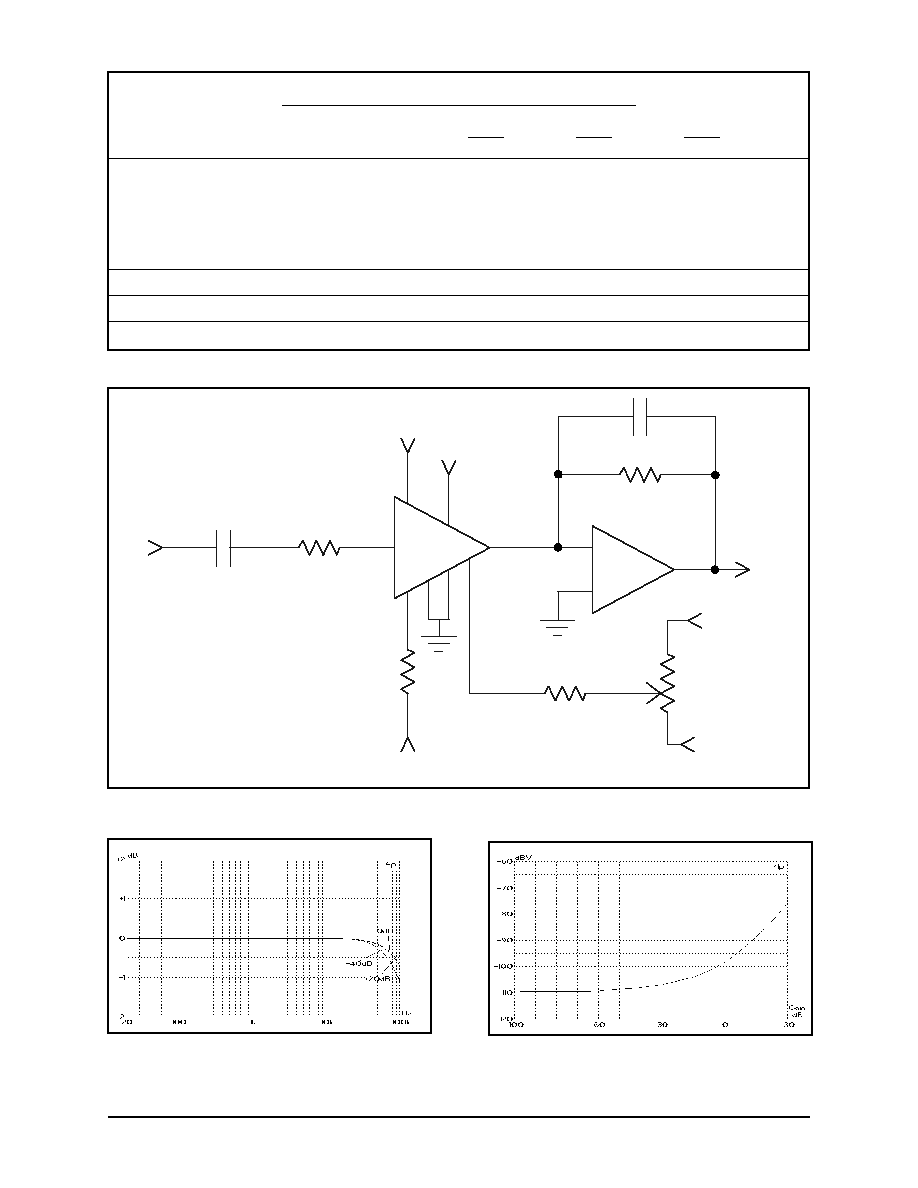
Figure 3. 2181 Series Frequency Response Vs. Gain
Figure 4. 2181 Series Noise (20kHz NBW) Vs. Gain
Vcc
Ec-
IN
10u
20k
5.1k
Vee
OUT
22p
20k
OUT
Vcc
Vee
50k SYM
ADJ
Rsym
OP275
7
3
8
4
2
6
5
1
V+
-IN
Ec-
Ec+
SYM
GND
V-
2181
Series
VCA
Power Supplies
Vcc = +15 V
Vee = -15 V
-
+
680k (2181A)
220k (2181B)
130k (2181C)
Figure 2. Typical Application Circuit

THAT Corporation; 45 Sumner Street; Milford, Massachusetts 01757-1656; USA
Tel: +1 508 478 9200; Fax: +1 508 478 0990; Web: www.thatcorp.com
Page 4
THAT2181 Series IC VCAs
Theory of Operation
3
The THAT 2181 Series VCAs are designed for high
performance in audio-frequency applications requiring
exponential gain control, low distortion, wide dynamic
range and low control-voltage feedthrough. These parts
control gain by converting an input current signal to a
bipolar logged voltage, adding a dc control voltage, and
re-converting the summed voltage back to a current
through a bipolar antilog circuit.
Figure 5 presents a considerably simplified internal
circuit diagram of the IC. The ac input signal current
flows in pin1, the input pin. An internal operational
transconductance amplifier (OTA) works to maintain
pin 1 at a virtual ground potential by driving the emitters
of Q1 and (through the Voltage Bias Generator) Q3.
Q3/D3 and Q1/D1 act to log the input current, producing
a voltage, V3, which represents the bipolar logarithm of
the input current. (The voltage at the junction of D1 and
D2 is the same as V3, but shifted by four forward V
be
drops.)
Gain Control
Since pin 8, the output, is usually connected to a vir-
tual ground, Q2/D2 and Q4/D4 take the bipolar antilog
of V3, creating an output current which is a precise rep-
lica of the input current. If pin 2 (Ec+) and pin 3 (Ec-)
are held at ground (with pin 4 - SYM - connected to a
high impedance current source), the output current will
equal the input current. For pin 2 positive or pin 3 nega-
tive, the output current will be scaled larger than the in-
put current. For pin 2 negative or pin 3 positive, the
output current is scaled smaller than the input.
The scale factor between the output and input cur-
rents is the gain of the VCA. Either pin 2 (Ec+) or pin 3
(Ec-), or both, may be used to control gain. Gain is expo-
nentially proportional to the voltage at pin 2, and expo-
nentially proportional to the negative of the voltage at
pin 3. Therefore, pin 2 (Ec+) is the positive control port,
while pin 3 (Ec-) is the negative control port. Because of
the exponential characteristic, the control voltage sets
gain linearly in decibels. Figure 6 shows the decibel cur-
rent gain of a 2181 versus the voltage at Ec+, while Fig-
ure 7 shows gain versus the Ec-.
Temperature Effects
The logging and antilogging in the VCA depends on
the logarithmic relationship between voltage and current
in a semiconductor junction (in particular, between a
transistor's V
be
and I
c
). As is well known, this relation-
3. For more details about the internal workings of the 2181 Series of VCAs, see An Improved Monolithic Volt-
age-Controlled Amplifier, by Gary K. Hebert (Vice-President, Engineering, for THAT Corporation), presented at the 99th
convention of the Audio Engineering Society, New York, Preprint number 4055.
Figure 6. Gain vs. Control Voltage (E
C+
, Pin 2) at 25∞C
Figure 7. Gain vs. Control Voltage (Ec-, Pin 3) at 25∞C
Figure 8. Gain vs. Control Voltage (Ec-) with Temp (∞C)
D1
IN
OUT
SYM
Ec-
D4
D3
Ec+
25
V-
+
Voltage
Bias
Generator
V
3
I
IN
Q1
Q4
Q3
Q2
Icell
Iadj
5
4
8
3
1
2
D2
Figure 5. Simplified Internal Circuit Diagram

ship is temperature dependent. Therefore, the gain of
any log-antilog VCA depends on its temperature.
Figure 8 shows the effect of temperature on the nega-
tive control port. (The positive control port behaves in the
same manner.) Note that the gain at Ec = 0 V is 0 dB, re-
gardless of temperature. Changing temperature changes
the scale factor of the gain by 0.33%/∞C, which pivots the
curve about the 0 dB point.
Mathematically, the 2181's gain characteristic is
Gain
E
E
(0.0061)(1 0.0033 T)
C
C
=
-
+
+
-
D
,
Eq. 1
where DT is the difference between room temperature
(25∞C) and the actual temperature, and Gain is the
gain in decibels. At room temperature, this reduces to
Gain
E
E
0.0061
C
C
=
-
+
-
,
Eq. 2
If only the positive control port is used, this becomes
Gain
E
0.0061
C
=
+
,
Eq. 3
If only the negative control port is used, this becomes
Gain
E
0.0061
C
=
-
-
,
Eq. 4
DC Bias Currents
The 2181 current consumption is determined by the
resistor between pin 5 (V-) and the negative supply voltage
(V
EE
). Typically, with 15V supplies, the resistor is 5.1 kW,
which provides approximately 2.4 mA. This current is
split into two paths: 570 mA is used for biasing the IC,
and the remainder becomes Icell as shown in Figure 5.
Icell is further split in two parts: about 20 mA biases the
core transistors (Q1 through Q4), the rest is available for
input and output signal current.
Trimming
The 2181-Series VCAs are intended to be adjusted for
minimum distortion by applying a small variable offset
voltage to pin 4, the SYM pin. Note that there is a 25 W re-
sistor internal to the 2181 between pin 4 and pin 2. As
shown in Figure 2, Page 3, the usual method of applying
this offset is to use the internal 25 W resistor along with a
larger value resistor to form a voltage divider connected
to the wiper of a trim pot across the supply rails.
This trim should be adjusted for minimum harmonic
distortion. This is usually done by applying a mid-
dle-level, middle-frequency signal (e.g. 1 kHz at 1 V) to
the audio input, setting the VCA to 0 dB gain, and adjust-
ing the SYM trim while observing THD at the output. In
the 2181, this adjustment coincides closely with the set-
ting
which
produces
minimum
control-voltage
feedthrough, though the two settings are not always iden-
tical.
DC Feedthrough
Normally, a small dc error term flows in pin 8 (the
output). When the gain is changed, the dc term changes.
This control-voltage feedthrough is more pronounced
with gain; the ≠A version of the part produces the least
feedthrough, the ≠C version the most. See Figure 9 for
typical curves for dc offset vs. gain
THAT Corporation; 45 Sumner Street; Milford, Massachusetts 01757-1656; USA
Tel: +1 508 478 9200; Fax: +1 508 478 0990; Web: www.thatcorp.com
600030 Rev 01
Page 5
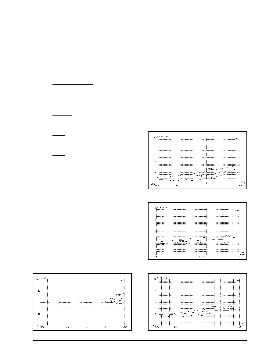
Figure 10. 1 kHz THD+Noise Vs. Input Level, 0 dB Gain
Figure 11. 1 kHz THD+Noise Vs. Input Level, +15 dB
Gain
Figure 9. Representative DC Offset Vs. Gain
Figure 12. 1 kHz THD+Noise Vs. Input Level, -15 dB
Gain


