 | –≠–ª–µ–∫—Ç—Ä–æ–Ω–Ω—ã–π –∫–æ–º–ø–æ–Ω–µ–Ω—Ç: THAT340 | –°–∫–∞—á–∞—Ç—å:  PDF PDF  ZIP ZIP |
THAT Corporation; 45 Sumner Street; Milford, Massachusetts 01757-1656; USA
Tel: +1 508 478 9200; Fax: +1 508 478 0990; Web: www.thatcorp.com
Document 600041 Rev 00
Low-Noise Matched Transistor Array ICs
FEATURES
∑
4 Matched NPN Transistors (300)
4 Matched PNP Transistors (320)
2 Matched NPNs and PNPs (340)
∑
Monolithic Construction
∑
Low Noise
- 0.75 nV
Hz (PNP)
- 0.8 nV
Hz (NPN)
∑
High Speed
- f
T
= 350 MHz (NPN)
- f
T
= 325 MHz (PNP)
∑
Excellent Matching ≠ 500
mV
typical between devices of same
gender
∑
Dielectrically Isolated for low
crosstalk and high DC isolation
∑
36V V
CEO
APPLICATIONS
∑
Microphone Preamplifiers
∑
Current Sources
∑
Current Mirrors
∑
Log/Antilog Amplifiers
∑
Multipliers
∑
Servos
DESCRIPTION
The
THAT
300
series
are
large-geometry,
4-transistor, monolithic NPN and/or PNP arrays ex-
hibiting both high speed and low noise, with excel-
lent parameter matching between transistors of the
same
gender.
With
typical
base-spreading
resistances of 25 ohms for the PNP devices
(30 ohms for the NPNs), their resulting low voltage
noise of under 1 nV/root-Hz makes the 300 series
ideally suited for low-noise amplifier input stages,
among other applications.
Fabricated in a dielectrically isolated, comple-
mentary bipolar process, each transistor is electri-
cally insulated from the others by a layer of
insulating oxide (not the reverse-biased PN junc-
tions used in conventional arrays) and exhibit
inter-device crosstalk and DC isolation similar to
that expected from discrete transistors. The result-
ing low collector-to-substrate capacitance produces
a typical NPN f
T
of 350 MHz (325 MHz for the
PNPs). Substrate biasing is not required for normal
operation, though the substrate should be grounded
to optimize speed and minimize crosstalk.
An eight-transistor bare-die array with similar
performance characteristics (the THAT 380G) is
also available from THAT Corporation. Please con-
tact us directly or through your local distributor for
more information.
T H A T
C o r p o r a t i o n
THAT 300 Series
Part Number
Configuration
Package
THAT300P
4-Matched NPN Transistors
DIP14
THAT300S
SO14
THAT320P
4- Matched PNP Transistors
DIP14
THAT320S
SO14
THAT340P
2 Matched NPN Transistors and
2 Matched PNP Transistors
DIP14
THAT340S
SO14
Table 1. Ordering Info
THAT Corporation; 45 Sumner Street; Milford, Massachusetts 01757-1656; USA
Tel: +1 508 478 9200; Fax: +1 508 478 0990; Web: www.thatcorp.com
Page 2
THAT300 Series Transistor Arrays
SPECIFICATIONS
1
Maximum Ratings (T
A
= 25∞C)
Parameter
Symbol
Conditions
Min
Typ
Max
Units
NPN Collector-Emitter Voltage
BV
CEO
I
C
= 1 mAdc, I
B
= 0
36
40
--
V
NPN Collector-Base Voltage
BV
CBO
I
C
=10
mAdc, I
E
=0
36
40
--
V
NPN Emitter-Base Voltage
BV
EBO
I
E
= 100
mAdc, I
C
= 0
5
--
--
V
NPN Collector Current
I
C MAX
10
20
mA
NPN Emitter Current
I
E MAX
10
20
mA
PNP Collector-Emitter Voltage
BV
CEO
I
C
= 1 mAdc, I
B
= 0
≠36
≠40
--
V
PNP Collector-Base Voltage
BV
CBO
I
C
= 10
mAdc, I
E
= 0
≠36
≠40
--
V
PNP Emitter-Base Voltage
BV
EBO
I
E
= 100
mAdc, I
C
= 0
≠5
--
--
V
PNP Collector Current
I
C MAX
≠10
≠20
mA
PNP Emitter Current
I
E MAX
≠10
≠20
mA
Collector-Collector Voltage
BV
CC
±100
±200
--
V
Emitter-Emitter Voltage
BV
EE
±100
±200
--
V
Operating Temperature Range
T
A
0
70
∞C
Maximum Junction Temperature
T
JMAX
150
∞C
Storage Temperature
T
STORE
-45
125
∞C
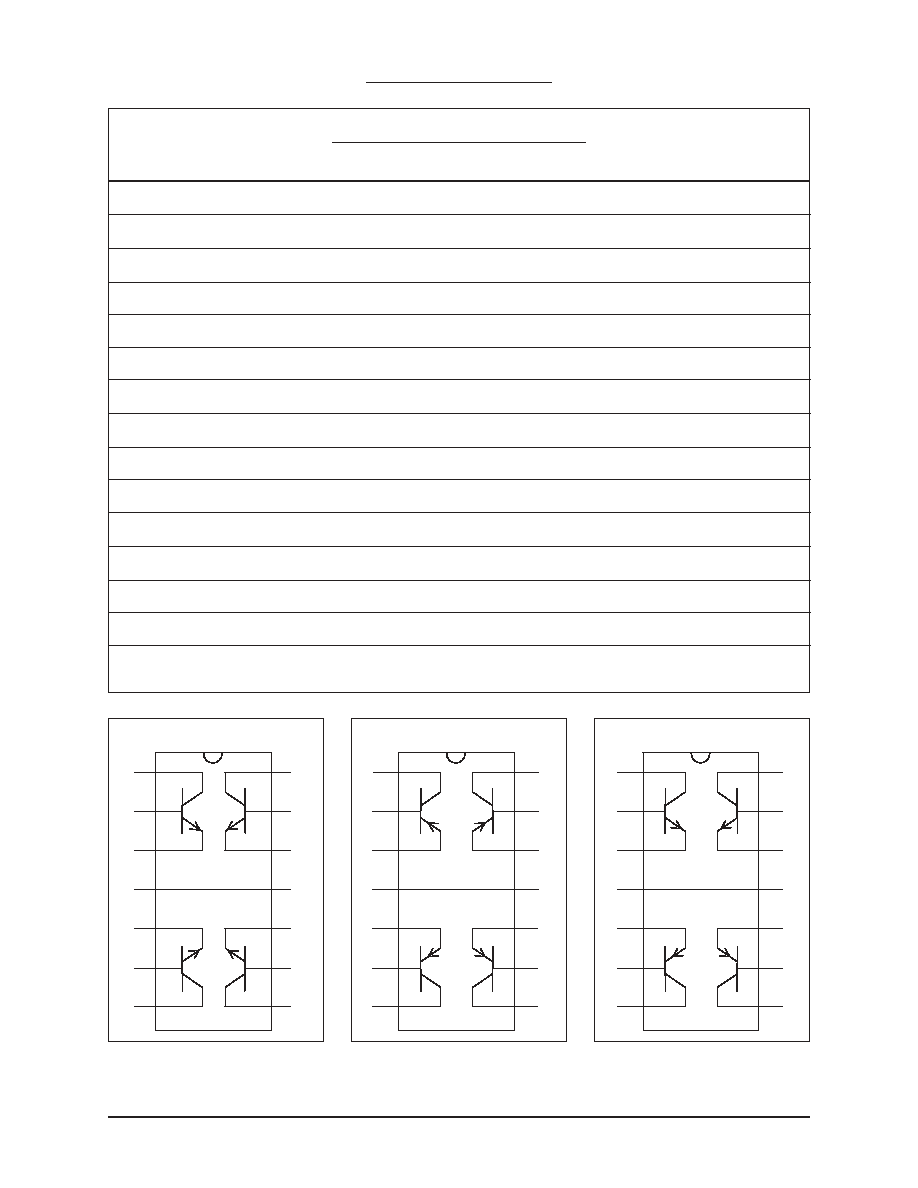
13
12
Q2
1
2
3
Q1
4
5
6
7
Q3
SUB
11
10
9
8
Q4
SUB
14
THAT 300
Fig 1. 300 Pinout
13
12
Q2
11
10
9
8
Q4
SUB
1
2
3
4
5
6
7
Q1
Q3
SUB
14
THAT 320
Fig 2. 320 Pinout
13
12
Q2
11
10
9
8
Q4
SUB
1
2
3
4
5
6
7
Q1
Q3
SUB
14
THAT 340
Fig 3. 340 Pinout
THAT Corporation; 45 Sumner Street; Milford, Massachusetts 01757-1656; USA
Tel: +1 508 478 9200; Fax: +1 508 478 0990; Web: www.thatcorp.com
600041 Rev 00
Page 3
1. All specifications subject to change without notice.
2. Unless otherwise noted, T
A
=25∞C.
SPECIFICATIONS
1
(Cont'd)
NPN Electrical Characteristics
2
Parameter
Symbol
Conditions
Min
Typ
Max
Units
NPN Current Gain
h
fe
V
CB
= 10 V
I
C
= 1 mA
60
100
--
I
C
= 10
mA
100
--
NPN Current Gain Matching
Dh
fe
V
CB
= 10 V, I
C
= 1 mA
--
5
--
%
NPN Noise Voltage Density
e
N
V
CB
= 10 V, I
C
= 1 mA, 1 kHz
--
0.8
--
nV
Hz
NPN Gain-Bandwidth Product
f
T
I
C
= 1 mA, V
CB
= 10 V
350
MHz
NPN
DV
BE
(THAT300: V
BE1
-V
BE2 ;
V
BE3
-V
BE4
) (THAT340: V
BE1
-V
BE2
)
V
OS
I
C
= 1 mA
--
±0.5
±3
mV
I
C
= 10
mA
--
±0.5
mV
NPN
DI
B
(THAT300: I
B1
-I
B2,
I
B3
-I
B4
) (THAT340: I
B1
-I
B2
)
I
OS
I
C
= 1 mA
--
±500
±1500
nA
I
C
= 10
mA
--
±5
nA
NPN Collector-Base Leakage Current I
CBO
V
CB
= 25 V
--
25
--
pA
NPN Bulk Resistance
r
BE
V
CB
= 0 V, 10
mA < I
C
< 10 mA
--
2
--
W
NPN Base Spreading Resistance
r
bb
V
CB
= 10 V, I
C
= 1 mA
--
30
--
W
NPN Collector Saturation Voltage
V
CE(SAT)
I
C
= 1 mA, I
B
= 100
mA
--
0.05
V
NPN Output Capacitance
C
OB
V
CB
= 10 V, I
E
= 0 mA, 100 kHz
3
pF
NPN Collector-CollectorCapacitance (THAT300: Q1-Q2, Q3-Q4) (THAT340: Q1-Q2)
C
CC
V
CC
= 0 V, 100 kHz
0.7
pF
PNP Electrical Characteristics
2
Parameter
Symbol
Conditions
Min
Typ
Max
Units
PNP Current Gain
h
fe
V
CB
= 10 V
I
C
= 1 mA
50
75
--
I
C
= 10
mA
75
--
PNP Current Gain Matching
Dh
fe
V
CB
= 10 V, I
C
= 1 mA
--
5
--
%
PNP Noise Voltage Density
e
N
V
CB
= 10 V, I
C
= 1 mA, 1 kHz
--
0.75
--
nV
Hz
PNP Gain-Bandwidth Product
f
T
I
C
= 1 mA, V
CB
= 10 V
325
MHz
PNP
DV
BE
(THAT320: V
BE1
-V
BE2;
V
BE3
-V
BE4
) (THAT340: V
BE3
-V
BE4
)
V
OS
I
C
= 1 mA
--
±0.5
±3
mV
I
C
= 10
mA
--
±0.5
mV
PNP
DI
B
(THAT320: I
B1
-I
B2;
I
B3
-I
B4
) (THAT340: I
B3
-I
B4
)
I
OS
I
C
= 1 mA
--
±700
±1800
nA
I
C
= 10
mA
--
±7
nA
PNP Collector-Base Leakage Current I
CBO
V
CB
= 25 V
--
≠25
--
pA

THAT Corporation; 45 Sumner Street; Milford, Massachusetts 01757-1656; USA
Tel: +1 508 478 9200; Fax: +1 508 478 0990; Web: www.thatcorp.com
Page 4
THAT300 Series Transistor Arrays
SPECIFICATIONS
1
(Cont'd)
PNP Bulk Resistance
r
BE
V
CB
= 0 V, 10
mA < I
C
< 10 mA
--
2
--
W
PNP Base Spreading Resistance
r
bb
V
CB
= 10 V, I
C
= 1 mA
--
25
--
W
PNP Collector Saturation Voltage
V
CE(SAT)
I
C
= 1 mA, I
B
= 100
mA
--
≠0.05
V
PNP Output Capacitance
C
OB
V
CB
= 10 V, I
E
= 0 mA, 100 kHz
3
pF
PNP Collector-Collector Capacitance (THAT320: Q1-Q2; Q3-Q4) (THAT340: Q3-Q4)
C
CC
V
CC
= 0 V, 100 kHz
0.6
pF
Information furnished by THAT Corporation is believed to be accurate and reliable. However no responsibility is as-
sumed by THAT Corporation for it's use nor for any infringements of patents or other rights of third parties which may
result from it's use.
LIFE SUPPORT POLICY
THAT Corporation products are not designed for use in life support equipment where malfunction of such products
can reasonably be expected to result in personal injury or death. The buyer uses or sells such products for life suport
application at the buyer's own risk and agrees to hold harmless THAT Corporation from all damages, claims, suits or
expense resulting from such use.
CAUTION: THIS IS AN ESD (ELECTROSTATIC DISCHARGE) SENSITIVE DEVICE.
It can be damaged by the currents generated by electrostatic discharge. Static charge and therefore dangerous volt-
ages can accumulate and discharge without detection causing a loss of function or performance to occur.
The transistors in this device are unprotected in order to maximize performance and flexibility. They are more sen-
sitive to ESD damage than many other ICs which include protection devices at their inputs. Note that all of the pins
(not just the "inputs") are susceptible.
Use ESD preventative measures when storing and handling this device. Unused devices should be stored in conduc-
tive packaging. Packaging should be discharged to the destination socket before the devices are removed. ESD damage
can occur to these devices even after they are installed in a board-level assembly. Circuits should include specific and
appropriate ESD protection.
0.750±0.004
(19.05±0.10)
0.25±.004
(6.35±0.10)
0.30 ±0.02
(7.62 ±0.5)
0.060
(1.52)
0.075
(1.91)
0.10 Typ.
(2.54)
0.018
(0.46)
0.125±0.004
(3.18±0.10)
Typ.
1
0.010
(0.25)
Note:
JA = 100 ∞C / W
q
Figure 4. Dual-In-Line Package Outline
0.050
(1.27)
Typ
0.245
(6.2)
Max
0.157
(3.99)
Max
0.018 (0.46)
Max
0.344 (8.74)
Max
0.069
(1.75)
Max
0.010
(0.25)
Max
1
Note:
JA = 100 ∞C / W
q
Figure 5. Surface-Mount Package Outline