 | –≠–ª–µ–∫—Ç—Ä–æ–Ω–Ω—ã–π –∫–æ–º–ø–æ–Ω–µ–Ω—Ç: THAT4320S | –°–∫–∞—á–∞—Ç—å:  PDF PDF  ZIP ZIP |

THAT Corporation; 45 Sumner Street; Milford, Massachusetts 01757-1656; USA
Tel: +1 508 478 9200; Fax: +1 508 478 0990; Web: www.thatcorp.com
Document 600045 Rev 00
T H A T
C o r p o r a t i o n
Pre-trimmed Low-voltage
Low-power Analog Engine
Æ
IC
THAT 4320S
FEATURES
∑ Pre-trimmed VCA & RMS detector
∑ Wide supply voltage range: 4.5V~16V
∑ Low supply current: 3.7mA typ. (5V)
∑ Four opamps
∑ One low-noise opamp (<5nV/rt-Hz)
∑ On board PTAT reference
∑ Wide dynamic range: 120dB as
compander
APPLICATIONS
∑ Companding noise reduction
∑
Wireless microphones
∑
Wireless instrument packs
∑
Wireless in-ear monitors
∑ Battery operated dynamics processors
∑
Compressors
∑
Limiters
∑
AGCs
∑
De-essers
Description
The THAT4320S is a single-chip Analog En-
gine
Æ
optimized for low-voltage, low-power oper-
ation. Incorporating a high-performance voltage-
controlled amplifier (VCA), RMS-level sensor,
and four opamps, the surface mount part is
aimed at battery-operated audio applications
such as wireless microphones, wireless instru-
ments and in-ear monitors. The 4320 operates
from a single supply voltage down to +4.5Vdc,
drawing only 3.7mA.
This IC also works at supply voltages up to
16Vdc, making it useful in line-operated prod-
ucts as well. The VCA is pre-trimmed at wafer
stage to deliver low distortion without further ad-
justment. And, one opamp is quiet enough to be
used as a microphone preamp.
The part was developed specifically for use as
a companding noise reduction system, drawing
from THAT's long history and experience with
dbx
Æ
technology for noise reduction. However,
with 22 active pins, the part is extremely flexible
and can be configured for a wide range of appli-
cations
including
single
and
multi-band
companders,
compressors,
limiters,
AGCs,
de-essers, etc.
What really sets the 4320 apart is the trans-
parent sound of its BlackmerTM VCA coupled
with its accurate true-RMS level detector. The IC
is useful in battery-powered mixers, compres-
sor/limiters, ENG devices and other portable au-
dio products. The part is highly integrated and
requires minimal external support circuitry: it
even contains an on-board PTAT (proportional to
absolute temperature) voltage reference to gener-
ate thermally compensated control voltages for
thresholds and gain settings.
26
27
23
21
20
18
THAT
4320S
OA1
EC-
EC+
IN
OUT
VCA
OA4
OA3
IN
CT
OUT
RMS
OA2
V
REF
GND
17
16
15
13
11
4
2
3
6
7
8
9
28
1
V
CC
V
EE
14
V
PTAT
25
V /2 Buffer
CC
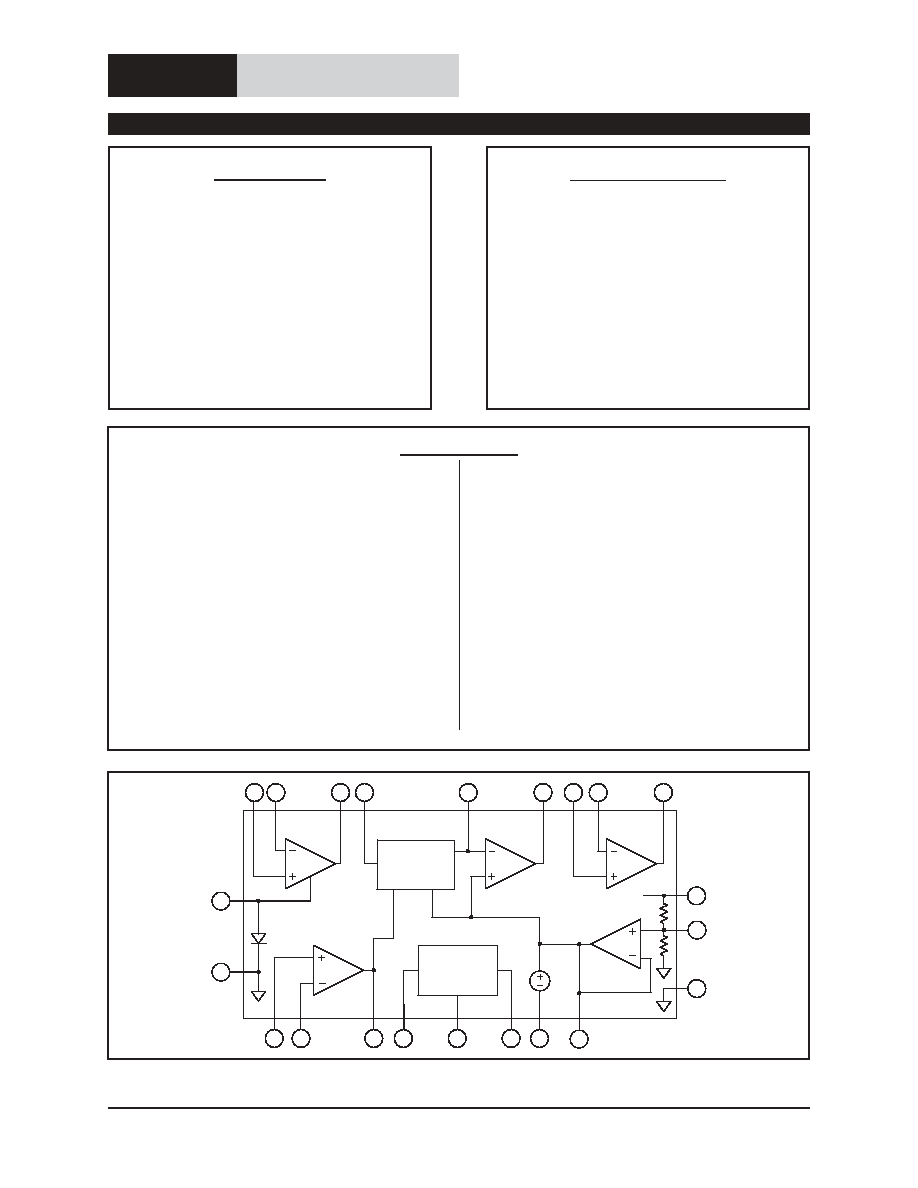
Figure 1. THAT4320S equivalent block diagram

THAT Corporation; 45 Sumner Street; Milford, Massachusetts 01757-1656; USA
Tel: +1 508 478 9200; Fax: +1 508 478 0990; Web: www.thatcorp.com
Page 2
THAT4320 Analog Engine
‚
Positive Supply Voltage (V
CC
)
+18V
Supply Current (I
CC
)
30mA
Operating Temperature Range (T
OP
)
-40 to +85 ∫C
Junction Temperature (T
J
)
-40 to +125 ∫C
Output Short-Circuit Duration
30 sec
Power Dissipation (P
D
) at T
A
=85 ∫C
400mW
Input Voltage
Supply Voltage
Storage Temperature Range (T
ST
)
-40 to +125 ∫C
Lead Temperature Range (Soldering, 10 sec)
300 ∫C
Absolute Maximum Ratings
1
Power Supply
Positive Supply Voltage
V
CC
Referenced to GND
+4.5
-
+16
V
Negative Supply Voltage (OA
1
)
V
EE
OA
1
only
V
CC
-16
0
0
V
Resistive Divider Voltage
V
PIN13
When overridden by split supply
V
CC
- 8
V
CC
/ 2
GND + 8
V
Supply Current
I
CC
No Signal
V
CC
=+5 V
3.7
6
mA
V
CC
=+15 V
5
10
mA
I
EE
V
CC
=+5V, V
EE
=-5 V
0.6
-
mA
Voltage Controlled Amplifier (VCA)
Max. I/O Signal Current i
IN(VCA)
or i
OUT(VCA)
V
CC
= +5 V
175
mA RMS
V
CC
= +15 V
350
mA RMS
Gain at 0V Control
3
G
0
0V at +IN of OA
2
-1.5
0
+1.5
dB
Gain-Control Constant
E
C+
/Gain (dB)
-60 dB < gain < +40 dB
-
6.0
-
mV/dB
Gain-Control Tempco
DE
C
/
DT
CHIP
Ref T
CHIP
=27∫C
-
+0.33
-
%/∫C
Output Offset Voltage Change
4
D V
OFF(OUT)
R
OUT
= 20 k
W
0 dB gain
-
1
15
mV
+15 dB gain
-
3
30
mV
+30 dB gain
-
10
50
mV
Output Noise
e
N(OUT)
0 dB gain
22Hz~22kHz, R
IN
=R
OUT
=20 k
W
-
-98
-95
dBV
Total Harmonic Distortion
3
THD
V
IN
= -5dBV, 1kHz, 0V at +IN of OA
2
0.05
0.1
%
RMS level detector
Output Voltage at Reference i
IN
e
O(0)
i
IN
= 7.5
mA RMS
-8
0
+8
mV
Output Error at Input Extremes
e
ORMS)error
i
IN
= 200 nA RMS
1
3
dB
i
IN
= 1mA RMS
1
3
dB
Electrical Characteristics
2
Parameter
Symbol
Conditions
Min
Typ
Max
Units
SPECIFICATIONS
1.
If the devices are subjected to stress above the Absolute Maximum Ratings, permanent damage may result.
Sustained operation at or near the Absolute Maximum Ratings conditions is not recommended. In particular, like all
semiconductor devices, device reliability declines as operating temperature increases.
2. Unless otherwise noted, T
A
=25∫C, V
CC
=+5V, V
EE
=0 V. Test circuit is as shown in Figure 2.
3. Assumes OA
2
is configured for unity gain, & includes offset voltage of OA
2
.
4. Reference is to output offset with -80dB VCA gain.

THAT Corporation; 45 Sumner Street; Milford, Massachusetts 01757-1656; USA
Tel: +1 508 478 9200; Fax: +1 508 478 0990; Web: www.thatcorp.com
Document 600045 Rev 00
Page 3
Scale Factor Match to VCA
-20 dB < VCA gain < +20 dB
1
ma< i
IN(RMS)
< 100
mA
.95
1
1.05
-
Rectifier Balance
±7.5mA DC
IN
±1
dB
Timing Current
I
T
-
7.5
-
mA
Filtering Time Constant
t
3467 X C
TIME
s
Output Tempco
DE
O
/
DT
CHIP
Ref T
CHIP
= 27 ∫C
-
+0.33
-
%/∫C
Load Resistance
R
L
-250mV < V
OUTRMS
< +250mV, re:Vref
2
k
W
Capacitive Load
C
L
150
pf
Operational Amplifier OA1
Input Offset Voltage
V
OS
-
± 1
± 3.5
mV
Input Bias Current
I
B
-
500
1200
nA
Input Offset Current
I
OS
-
± 30
± 120
nA
Input Common Mode Range
V
ICR+
4
4.3
-
V
V
ICR-
-
0.4
0.6
V
Equivalent Input Noise Voltage e
N(IN)
f = 1 kHz
-
4.5
6
nv/
÷
Hz
Equivalent Input Noise Current i
N(IN)
f = 1 kHz
-
0.9
-
pA/
÷
Hz
Gain Bandwidth Product
GBW
f = 50 kHz
-
18
-
MHz
Slew Rate
SR
G = +10, C
L
= 100 pf
3.5
5.8
-
V/
ms
Open Loop Gain
A
VOL
R
L
= 10 k
W
-
95
-
dB
Output Short Circuit Current
I
SC+
Output to V
CC
/2, V
ID
= +0.4 V
-2.3
-6.5
-20
mA
I
SC-
Output to V
CC
/2, V
ID
= -0.4 V
1.5
3.7
10
mA
Output Voltage Range
V
O+
R
L
= 10 k
W to V
CC
/2, G = +10
V
CC
-0.9 V
CC
-0.75
-
V
V
O+
V
EE
+0.75 V
EE
+0.95
V
Capacitive Load
C
L
150
pf
Power Supply Rejection Ratio PSRR
+5 V < V
CC
-V
EE
< +15V
-
105
-
dB
Operational Amplifier OA2 (Control Voltage Buffer)
Input Offset Voltage
V
OS
-
± 1.5
± 6
mV
Input Bias Current
I
B
-
450
1000
nA
Input Offset Current
I
OS
-
± 25
± 100
nA
Input Common Mode Range
V
ICR
-1
+1
V
Equivalent Input Noise Voltage e
N(IN)
f = 1 kHz
-
8
-
nv/
÷
Hz
Equivalent Input Noise Current i
N(IN)
f = 1 kHz
-
0.6
-
pA/
÷
Hz
Gain Bandwidth Product
GBW
f = 50 kHz, C
L
= 100 nf, R
L
= 10 k
W
-
0.12/C
L
-
Hz
Slew Rate
SR
G = +1
I
SC
/C
L
-
V/
ms
Electrical Characteristics (con't)
2
Parameter
Symbol
Conditions
Min
Typ
Max
Units

THAT Corporation; 45 Sumner Street; Milford, Massachusetts 01757-1656; USA
Tel: +1 508 478 9200; Fax: +1 508 478 0990; Web: www.thatcorp.com
Page 4
THAT4320 Analog Engine
‚
Open Loop Gain
A
VOL
R
L
= 10 k
W
-
57.5
dB
20*log(.075*RI)
dB
Output Short Circuit Current
I
SC+
Output to V
CC
/2, V
ID
= +0.4 V
-
-4
-
mA
I
SC-
Output to V
CC
/2, V
ID
= -0.4 V
-
2.7
-
mA
Power Supply Rejection Ratio PSRR
+5 V < V
CC
< +15 V
-
88
-
dB
Capacitive Load
5
C
L
22
nf
Operational Amplifier OA3 (VCA Current-to-Voltage Converter)
Input Offset Voltage
V
OS
± 1.5
mV
Input Bias Current
I
B
-
200
nA
Input Offset Current
I
OS
Only one input is accessible
Input Common Mode Range
V
ICR
Not meaningful
Equivalent Input Noise Voltage e
N(IN)
f = 1 kHz
-
10.5
-
nv/
÷
Hz
Equivalent Input Noise Current i
N(IN)
f = 1 kHz
-
0.3
-
pA/
÷
Hz
Gain Bandwidth Product
GBW
f = 50 kHz
-
9
-
MHz
Slew Rate
SR
C
L
= 100 pf
-
3.75
-
V/
ms
Open Loop Gain
A
VOL
R
L
= 10 k
W
-
92
-
dB
Output Short Circuit Current
I
SC+
Output to V
CC
/2
-3.5
-
mA
I
SC-
2.5
-
mA
Output Voltage Range
R
L
= 10 k
W to V
CC
/2, Rf = 20 k
W, 0 dB VCA gain
V
O+
I
in(VCA)
= +100
mA
4.1
4.25
-
V
V
O+
I
in(VCA)
= -100
mA
0.75
0.9
V
Capacitive Load
C
L
150
pf
Operational Amplifier OA4
Input Offset Voltage
V
OS
-
± 1.5
± 5
mV
Input Bias Current
I
B
-
200
500
nA
Input Offset Current
I
OS
-
± 10
± 50
nA
Input Common Mode Range
V
ICR+
4
4.3
-
V
V
ICR-
-
0.4
0.6
V
Equivalent Input Noise Voltage e
N(IN)
f = 1 kHz
-
10.5
14
nv/
÷
Hz
Equivalent Input Noise Current i
N(IN)
f = 1 kHz
-
0.3
-
pA/
÷
Hz
Gain Bandwidth Product
GBW
f = 50 kHz
-
9
-
MHz
Slew Rate
SR
G = +10, C
L
= 100 pf
2.2
3.75
-
V/
ms
Open Loop Gain
A
VOL
R
L
= 10 k
W
-
92
-
dB
Electrical Characteristics (con't)
2
Parameter
Symbol
Conditions
Min
Typ
Max
Units
5
Note - OA
2
and the V
CC
/2 buffer require a capacitve load for stability.

THAT Corporation; 45 Sumner Street; Milford, Massachusetts 01757-1656; USA
Tel: +1 508 478 9200; Fax: +1 508 478 0990; Web: www.thatcorp.com
Document 600045 Rev 00
Page 5
Output Short Circuit Current
I
SC+
Output to V
CC
/2, V
ID
= +0.4 V
-1.3
-3.5
-12
mA
I
SC-
Output to V
CC
/2, V
ID
= -0.4 V
1
2.5
8
mA
Output Voltage Range
V
O+
R
L
= 10 k
W to V
CC
/2, G = +10
4.1
4.25
-
V
V
O+
0.75
0.9
V
Capacitive Load
C
L
150
pf
Power Supply Rejection Ratio PSRR
+5V < V
CC
< +15 V
-
100
-
dB
Vcc/2 Reference Buffer
Reference Voltage
V
REF
No Signal, No load on pin 13,
V
CC
= +5 V, R
L
= 3 k
W to V
CC
or GND
2.4
2.5
2.6
V
V
CC
= +15 V
-
V
CC
/2
-
V
Voltage Divider Impedance
R
A
, R
B
-
20
-
k
W
Output Short Circuit Current
I
Osc-
Output to V
CC
-3
mA
I
Osc+
Output to GND
4.5
mA
Output Noise Voltage
e
N(OUT)
22 Hz ~ 22 kHz, C
FILT
= 22
mf
-
-120
-117
dBV
Capacitive Load
5
C
L
22
nf
Proportional To Absolute Temperature (PTAT) Voltage Generator
Output Voltage
V
PTAT
R
L
= 10 k
W, T
CHIP
= 25 ∫C
-
V
REF
- 0.072
-
V
VCA Gain Change Caused by V
PTAT
V
PTAT
applied to OA
2
, A
V
= +1
VCA Gain at 1 kHz
-11
-12
-13
dB
Output Tempco
D
(V
PTAT
-V
REF
)/
D
T
CHIP
Ref T
CHIP
= 27 ∫C
-
+0.33
-
%/∫C
Maximum Sink Current
I
SINK(MAX)
800
mA
Capacitive Load
C
L
150
pf
Performance as a Compander
6
(through an encode-decode cycle)
Dynamic Range
(Max signal level) - (No Signal Output Noise)
120
dB
Distortion
THD
f = 1 kHz
0.1
%
Frequency response
-20 dB re: Max Signal
20 Hz ~ 20 kHz
±
1.5
dB
Electrical Characteristics (con't)
2
Parameter
Symbol
Conditions
Min
Typ
Max
Units
Surface Mount Package
Type
See page 16 for pinout and dimensions
28-Pin QSOP
Thermal Resistance
q
JC
SO package in ambient
-
30
-
∫C/W
Thermal Resistance
q
JA
SO package soldered to board
-
90
-
∫C/W
Soldering Reflow Profile
JEDEC JESD22-A113-B (220 ∫C)
Package Characteristics
Parameter
Symbol
Conditions
Min
Typ
Max
Units
6
Compressor circuit is as shown in Figure 12, Expander circuit is as shown in Figure 13.


