
THC63LVD104S Rev.1.0
Copyright 2004 THine Electronics, Inc. All rights reserved 1 THine Electronics, Inc.
THC63LVD104S
112MHz 30Bits Color LVDS Receiver
General Description
The THC63LVD104S receiver is designed to support
pixel data transmission between Host and Flat Panel
Display from NTSC up to SXGA resolutions. The
THC63LVD104S converts the LVDS data streams back
into 35bits of CMOS/TTL data with rising edge or fall-
ing edge clock for convenient with a variety of LCD
panel controllers.At a transmit clock frequency of
112MHz, 30bits of RGB data and 5bits of timing and
control data (HSYNC,VSYNC,DE,CNTL1,CNTL2)
are transmitted at an effective rate of 784Mbps per
LVDS channel.Using a 112MHz clock, the data
throughput is 490Mbytes per second.
Features
∑
Wide dot clock range: 8-112MHz suited for NTSC,
VGA, SVGA, XGA, and SXGA
∑
PLL requires no external components
∑
50% output clock duty cycle
∑
TTL clock edge and position programmable(3 step)
∑
Power down mode
∑
Low power single 2.5V CMOS design
∑
TQFP 64pin
∑
Pin compatible with THC63LVD104A
∑
Fail-safe for Open CLK Input
Block Diagram
LVDS INPUT
CMOS/TTL OUTPUT
RCLK+/-
(8 to112MHz)
PLL
RA+/-
RB+/-
RC+/-
RD+/-
RE+/-
DK
PD
OE
RA6-RA0
RB6-RB0
RC6-RC0
RD6-RD0
RE6-RE0
CLKOUT
S
E
R
I
A
L
T
O
P
A
R
A
L
L
E
L
CMOS/TTL INPUT
7
7
7
7
7
R/F

Copyright 2004 THine Electronics, Inc. All rights reserved 2 THine Electronics, Inc.
THC63LVD104S Rev.1.0
Pin Out
RB6
CLKOUT
GND
RC0
RC1
RC2
RC3
RC4
RC5
VCC
RC6
RD0
RD1
RD2
RD3
RD4
G
N
D
D
K
P
D
O
E
R
/
F
R
E
6
R
E
5
R
E
4
V
C
C
R
E
3
R
E
2
R
E
1
R
E
0
R
D
6
R
D
5
G
N
D
RA-
RA+
RB-
RB+
LVCC
RC-
RC+
RCLK-
RCLK+
LGND
RD-
RD+
RE-
RE+
PGND
PVCC
V
C
C
R
A
0
R
A
1
R
A
2
G
N
D
R
A
3
R
A
4
R
A
5
R
A
6
R
B
0
R
B
1
V
C
C
R
B
2
R
B
3
R
B
4
R
B
5
1 2 3
4 5 6
7 8 9 10
1
1 12 13 14 15 16
32
31
30
29
28
27
26
25
24
23
22
21
20
19
18
17
4
8 47 46 45 44 43 42 41 40 39 38 37 36 35 34 33
49
50
51
52
53
54
55
56
57
58
59
60
61
62
63
64

Copyright 2004 THine Electronics, Inc. All rights reserved 3 THine Electronics, Inc.
THC63LVD104S Rev.1.0
Pin Description
Pin Name
Pin No.
I/O Type
Description
RA+, RA-
50, 49
LVDS IN
LVDS Data In.
RB+, RB-
52, 51
LVDS IN
RC+, RC-
55, 54
LVDS IN
RD+, RD-
60, 59
LVDS IN
RE+,RE-
62, 61
LVDS IN
RCLK+, RCLK-
57, 56
LVDS IN
LVDS Clock In.
RA6 ~ RA0
40,41,42,43,45,46,47
OUT
CMOS/TTL Data Outputs.
RB6 ~ RB0
32,33,34,35,36,38,39
OUT
RC6 ~ RC0
22,24,25,26,27,28,29
OUT
RD6 ~ RD0
14,15,17,18,19,20,21
OUT
RE6 ~ RE0
6,7,8,10,11,12,13
OUT
PD
3
IN
Power down and Output Control.(Table1)
H: Normal operation
L: Power down
OE
4
IN
Output Enable. See Table1.
H:Output enable.
L:Output disable
DK
2
IN
( 3-Level )
Output Clock Delay Timing Select.(Fig5)
t
RCP
=Output Clock Cycle
L: Offset 0[nsec]
M: Offset -
(typ) [nsec]
H: Offset +
(typ)[nsec]
R/F
5
IN
Output Clock Triggering Edge Select.(Fig5)
H: Rising Edge
L: Falling Edge
VCC
9,23,37,48
Power
Power Supply Pins for TTL outputs and digital
circuitry.
CLKOUT
31
OUT
Clock out.
GND
1,16,30,44
Ground
Ground Pins for TTL outputs and digital circuitry.
LVCC
53
Power
Power Supply Pin for LVDS inputs.
LGND
58
Ground
Ground Pin for LVDS inputs.
PVCC
64
Power
Power Supply Pin for PLL circuitry.
PGND
63
Ground
Ground Pin for PLL circuitry.
3
tRCP
14
--------------
3
tRCP
14
--------------
Copyright 2004 THine Electronics, Inc. All rights reserved 4 THine Electronics, Inc.
THC63LVD104S Rev.1.0
Pin Description
(Continued)
Table 1. Output Control
** Rxn x = A,B,C,D,E n = 0,1,2,3,4,5,6
Absolute Maximum Ratings
Recommended Operating Conditions
PD
OE
Data Outputs
(Rxn)
CLKOUT
L
L
Hi-Z
Hi-Z
L
H
All Low
Fixed Low
H
L
Hi-Z
Hi-Z
H
H
Data Out
CLK Out
Supply Voltage (V
CC
)
-0.3V ~ +3.0V
CMOS/TTL Input Voltage
-0.3V ~ (V
CC
+ 0.3V)
CMOS/TTL Output Voltage
-0.3V ~ (V
CC
+ 0.3V)
LVDS Receiver Input Voltage
-0.3V ~ (V
CC
+ 0.3V)
Output Current
-30mA ~ 30mA
Junction Temperature
+125
Storage Temperature Range
-55
~ +150
Resistance to soldering heat
+260
/10sec
Maximum Power Dissipation @+25
1.4W
Parameter
Min
Typ
Max
Units
All Supply Voltage
2.3
2.5
2.7
V
Operating Ambient Temperature
0
70
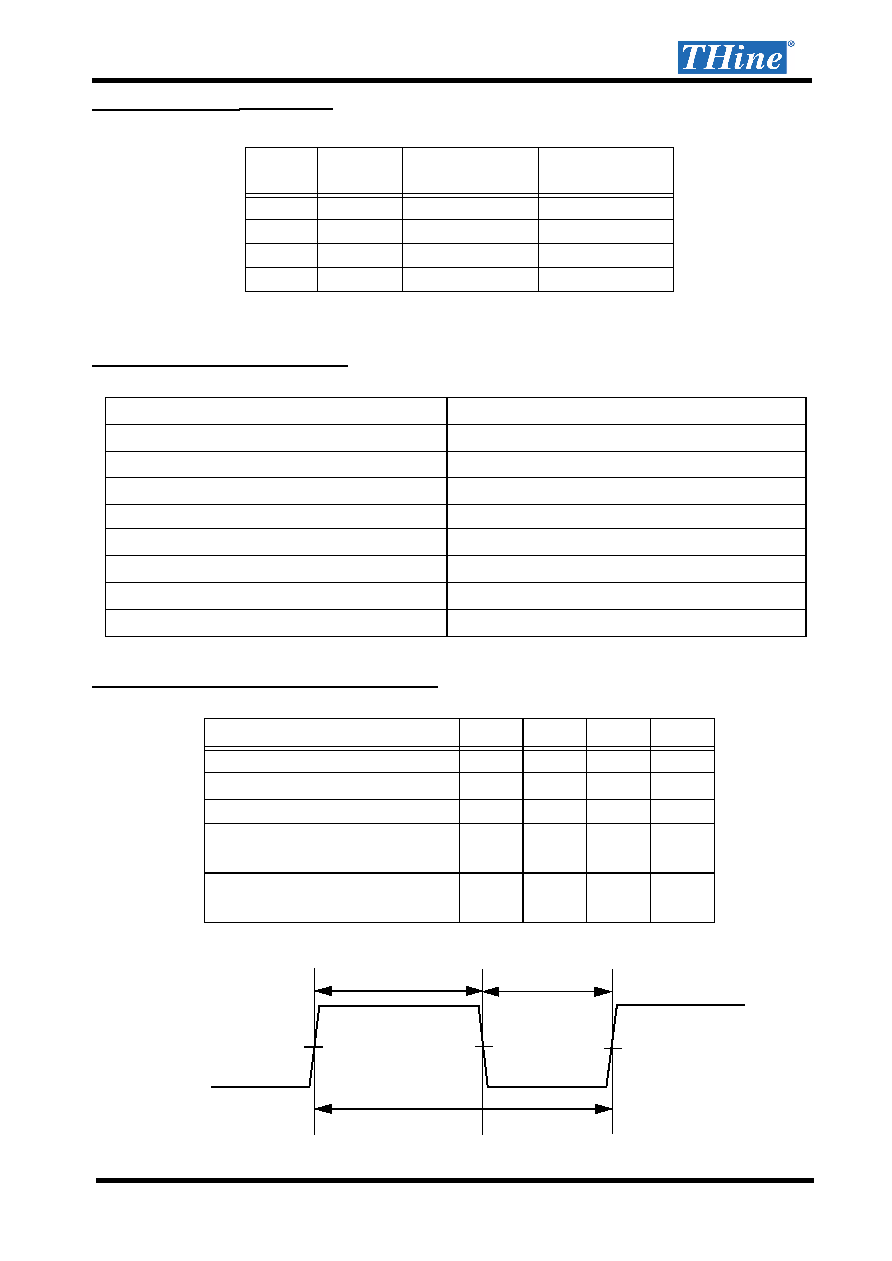
Differential CLKIN Frequency
8
112
MHz
Differential CLKIN High Time(
t
RCIH
)
(Fig1)
nsec
Differential CLKIN Low Time(
t
RCIL
)
(Fig1)
nsec
∞C
∞C
∞C
∞C
∞C
∞C
2
tRCIP
7
----------------
5
tRCIP
7
----------------
2
tRCIP
7
----------------
5
tRCIP
7
----------------
V
diff
= 0V
V
diff
= 0V
RCLK+
(Differential)
t
RCIH
V
diff
= 0V
t
RCIL
Fig1. Differential CLKIN
t
RCIP
Copyright 2004 THine Electronics, Inc. All rights reserved 5 THine Electronics, Inc.
THC63LVD104S Rev.1.0
Electrical Characteristics
CMOS/TTL DC Specifications
V
CC
=VCC=PVCC=LVCC
LVDS Receiver DC Specifications
V
CC
=VCC=PVCC=LVCC
Supply Current
V
CC
=VCC=PVCC=LVCC
Symbol
Parameter
Conditions
Min
Typ
Max
Units
V
IH
High Level Input Voltage
PD, OE,R/F Pin
1.7
V
CC
V
V
IL
Low Level Input Voltage
GND
0.7
V
V
IH3
High Level Input Voltage
3-Level Inputs(DK Pin)
2.1
V
CC
V
V
IM3
Middle Level Input Voltage
1.05
1.25
1.45
V
V
IL3
Low Level Input Voltage
GND
0.4
V
V
OH
High Level Output Voltage
I
OH
= -2mA
2.1
V
V
OL
Low Level Output Voltage
I
OL
= 2mA
0.4
V
I
IL
Input Leakage Current
PD, OE,R/F Pin
uA
I
IL3
3-Level Input Leakage Current
3-Level Inputs(DK Pin)
uA
Symbol
Parameter
Conditions
Min
Typ
Max
Units
V
TH
Differential Input High Threshold
V
IC
= 1.2V
100
mV
V
TL
Differential Input Low Threshold
V
IC
= 1.2V
-100
mV
I
ILD
Differential Input Leakage Current
V
IN
= 2.4V / 0V
uA
Symbol
Parameter
Conditions
Min
Typ
Max
Units
I
RCCW
Receiver Supply Current
Checker Pattern(Worst Case)
(Fig 2)
f
CLKOUT
=65MHz
CL=8pF
125
mA
f
CLKOUT
=85MHz
152
mA
f
CLKOUT
=112MHz
184
mA
I
RCCS
Receiver Power Down
Supply Current
PD = L, Ta=RT
10
uA
0V V
IN
V
CC
£
£
10
±
0V V
IN
V
CC
£
£
10
±
200
±