54ACT16543, 74ACT16543
16-BIT REGISTERED TRANSCEIVERS
WITH 3-STATE OUTPUTS
SCAS126B ≠ MARCH 1990 ≠ REVISED APRIL 1996
1
POST OFFICE BOX 655303
∑
DALLAS, TEXAS 75265
D
Members of the Texas Instruments
Widebus
TM
Family
D
Inputs Are TTL-Voltage Compatible
D
3-State True Outputs
D
Flow-Through Architecture Optimizes
PCB Layout
D
Distributed V
CC
and GND Pin
Configurations Minimize High-Speed
Switching Noise
D
EPIC
t
(Enhanced-Performance Implanted
CMOS) 1-
m
m Process
D
500-mA Typical Latch-Up Immunity at
125
∞
C
D
Package Options Include Plastic Thin
Shrink Small-Outline (DGG) and 300-mil
Shrink Small-Outline (DL) Packages Using
25-mil Center-to-Center Pin Spacings, and
380-mil Fine-Pitch Ceramic Flat (WD)
Packages Using 25-mil Center-to-Center
Pin Spacings
description
The 'ACT16543 are 16-bit registered transceivers
that contain two sets of D-type latches for
temporary storage of data flowing in either
direction. The 'ACT16543 can be used as two
8-bit transceivers or one 16-bit transceiver.
Separate latch enable (LEAB or LEBA) and
output-enable (OEAB or OEBA) inputs are
provided for each register to permit independent
control in either direction of data flow.
The A-to-B enable (CEAB) and OEAB inputs must
be low to enter data from A or to output data to B.
Having CEAB low and LEAB low makes the
A-to-B latches transparent; a subsequent low-to-
high transition at LEAB puts the A latches in the
storage mode. Data flow from B to A is similar, but
requires using the CEBA, LEBA, and OEBA
inputs.
The 74ACT16543 is packaged in TI's shrink small-outline package, which provides twice the functionality of
standard small-outline packages in the same printed-circuit-board area.
The 54ACT16543 is characterized for operation over the full military temperature range of ≠55
∞
C to 125
∞
C. The
74ACT16543 is characterized for operation from ≠40
∞
C to 85
∞
C.
Copyright
©
1996, Texas Instruments Incorporated
UNLESS OTHERWISE NOTED this document contains PRODUCTION
DATA information current as of publication date. Products conform to
specifications per the terms of Texas Instruments standard warranty.
Production processing does not necessarily include testing of all
parameters.
Please be aware that an important notice concerning availability, standard warranty, and use in critical applications of
Texas Instruments semiconductor products and disclaimers thereto appears at the end of this data sheet.
EPIC and Widebus are trademarks of Texas Instruments Incorporated.
1
2
3
4
5
6
7
8
9
10
11
12
13
14
15
16
17
18
19
20
21
22
23
24
25
26
27
28
56
55
54
53
52
51
50
49
48
47
46
45
44
43
42
41
40
39
38
37
36
35
34
33
32
31
30
29
1OEAB
1LEAB
1CEAB
GND
1A1
1A2
V
CC
1A3
1A4
1A5
GND
1A6
1A7
1A8
2A1
2A2
2A3
GND
2A4
2A5
2A6
V
CC
2A7
2A8
GND
2CEAB
2LEAB
2OEAB
1OEBA
1LEBA
1CEBA
GND
1B1
1B2
V
CC
1B3
1B4
1B5
GND
1B6
1B7
1B8
2B1
2B2
2B3
GND
2B4
2B5
2B6
V
CC
2B7
2B8
GND
2CEBA
2LEBA
2OEBA
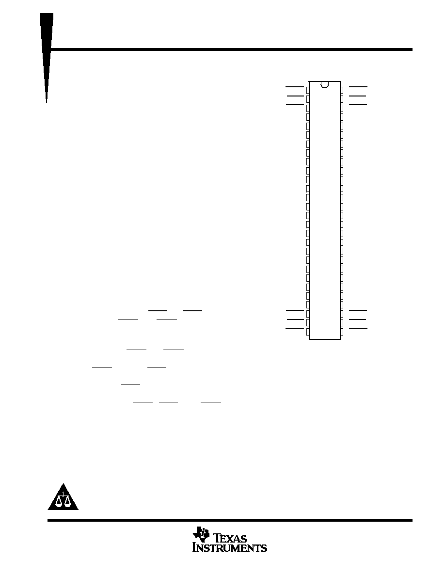
54ACT16543 . . . WD PACKAGE
74ACT16543 . . . DGG OR DL PACKAGE
(TOP VIEW)

54ACT16543, 74ACT16543
16-BIT REGISTERED TRANSCEIVERS
WITH 3-STATE OUTPUTS
SCAS126B ≠ MARCH 1990 ≠ REVISED APRIL 1996
2
POST OFFICE BOX 655303
∑
DALLAS, TEXAS 75265
FUNCTION TABLE
(each octal register)
INPUTS
LATCH
STATUS
OUTPUT
BUFFERS
CEAB
LEAB
OEAB
STATUS
A TO B
BUFFERS
B1≠B8
H
X
X
Storing
Z
X
H
X
Storing
X
X
H
Z
L
L
L
Transparent
Current A data
L
H
L
Storing
Previous A data
}
A-to-B data flow is shown: B-to-A flow control is the same except that
it uses CEBA, LEBA, and OEBA.
Data present before low-to-high transition of LEAB occurring while
CEAB is low

54ACT16543, 74ACT16543
16-BIT REGISTERED TRANSCEIVERS
WITH 3-STATE OUTPUTS
SCAS126B ≠ MARCH 1990 ≠ REVISED APRIL 1996
3
POST OFFICE BOX 655303
∑
DALLAS, TEXAS 75265
logic symbol
1A2
6
1A3
8
1A4
9
1A5
10
1A6
12
1A7
13
1A8
14
2A2
16
2A3
17
2A4
19
2A5
20
2A6
21
2A7
23
2A8
24
15
2A1
8C12
27
5
1A1
6D
1B6
45
1B7
44
1B8
43
1B2
51
1B3
49
1B4
48
1B5
47
1B1
52
5D
3
4
G8
26
8EN10
28
7C11
30
G7
31
7EN9
29
2C6
2
G2
3
2EN4
1
1C5
55
G1
54
1EN3
56
12D
2B6
36
2B7
34
2B8
33
2B2
41
2B3
40
2B4
38
2B5
37
2B1
42
11D
9
10
1OEBA
1CEBA
1LEBA
1OEAB
1CEAB
1LEAB
2OEBA
2CEBA
2LEBA
2OEAB
2CEAB
2LEAB
This symbol is in accordance with ANSI/IEEE Std 91-1984 and IEC Publication 617-12.
54ACT16543, 74ACT16543
16-BIT REGISTERED TRANSCEIVERS
WITH 3-STATE OUTPUTS
SCAS126B ≠ MARCH 1990 ≠ REVISED APRIL 1996
4
POST OFFICE BOX 655303
∑
DALLAS, TEXAS 75265
logic diagram (positive logic)
1OEBA
1CEBA
1LEBA
1OEAB
1CEAB
1LEAB
1A1
1B1
To Seven Other Channels
2OEBA
2CEBA
2LEBA
2OEAB
2CEAB
2LEAB
2A1
2B1
To Seven Other Channels
56
54
55
1
3
2
5
29
31
30
28
26
27
15
C1
1D
C1
1D
C1
1D
C1
1D
42
52
54ACT16543, 74ACT16543
16-BIT REGISTERED TRANSCEIVERS
WITH 3-STATE OUTPUTS
SCAS126B ≠ MARCH 1990 ≠ REVISED APRIL 1996
5
POST OFFICE BOX 655303
∑
DALLAS, TEXAS 75265
absolute maximum ratings over operating free-air temperature range (unless otherwise noted)
Supply voltage range, V
CC
≠0.5 V to 7 V
. . . . . . . . . . . . . . . . . . . . . . . . . . . . . . . . . . . . . . . . . . . . . . . . . . . . . . . . . .
Input voltage range, V
I
(see Note 1)
≠0.5 V to V
CC
+0.5 V
. . . . . . . . . . . . . . . . . . . . . . . . . . . . . . . . . . . . . . . . . . . . .
Output voltage range, V
O
(see Note 1)
≠0.5 V to V
CC
+0.5 V
. . . . . . . . . . . . . . . . . . . . . . . . . . . . . . . . . . . . . . . . . .
Input clamp current, I
IK
(V
I
< 0 or V
I
> V
CC
)
±
20 mA
. . . . . . . . . . . . . . . . . . . . . . . . . . . . . . . . . . . . . . . . . . . . . . . . .
Output clamp current, I
OK
(V
O
< 0 or V
O
> V
CC
)
±
50 mA
. . . . . . . . . . . . . . . . . . . . . . . . . . . . . . . . . . . . . . . . . . . .
Continuous output current, I
O
(V
O
= 0 to V
CC
)
±
50 mA
. . . . . . . . . . . . . . . . . . . . . . . . . . . . . . . . . . . . . . . . . . . . . .
Continuous current through V
CC
or GND
±
400 mA
. . . . . . . . . . . . . . . . . . . . . . . . . . . . . . . . . . . . . . . . . . . . . . . . . .
Maximum power dissipation at T
A
= 55
∞
C (in still air) (see Note 2): DGG package
1 W
. . . . . . . . . . . . . . . . . .
DL package
1.4 W
. . . . . . . . . . . . . . . . . . .
Storage temperature range, T
stg
≠65
∞
C to 150
∞
C
. . . . . . . . . . . . . . . . . . . . . . . . . . . . . . . . . . . . . . . . . . . . . . . . . . . .
Stresses beyond those listed under "absolute maximum ratings" may cause permanent damage to the device. These are stress ratings only, and
functional operation of the device at these or any other conditions beyond those indicated under "recommended operating conditions" is not
implied. Exposure to absolute-maximum-rated conditions for extended periods may affect device reliability.
NOTES:
1. The input and output voltage ratings may be exceeded if the input and output current ratings are observed.
2. The maximum package power dissipation is calculated using a junction temperature of 150
_
C and a board trace length of 750 mils.
recommended operating conditions (see Note 3)
54ACT16543
74ACT16543
UNIT
MIN
NOM
MAX
MIN
NOM
MAX
UNIT
VCC
Supply voltage (see Note 4)
4.5
5
5.5
4.5
5
5.5
V
VIH
High-level input voltage
2
2
V
VIL
Low-level input voltage
0.8
0.8
V
VI
Input voltage
0
VCC
0
VCC
V
VO
Output voltage
0
VCC
0
VCC
V
IOH
High-level output current
≠24
≠24
mA
IOL
Low-level output current
24
24
mA
D
t/
D
v
Input transition rise or fall rate
0
10
0
10
ns/V
TA
Operating free-air temperature
≠55
125
≠40
85
∞
C
NOTES:
3. Unused pins (inputs and I/O) must be held high or low to prevent them from floating.
4. All VCC and GND pins must be connected to the proper voltage power supply.
PRODUCT PREVIEW information concerns products in the formative or
design phase of development. Characteristic data and other
specifications are design goals. Texas Instruments reserves the right to
change or discontinue these products without notice.