54ACT16833, 74ACT16833
DUAL 8-BIT TO 9-BIT PARITY BUS TRANSCEIVERS
SCAS166A ≠ JUNE 1990 ≠ REVISED APRIL 1996
1
POST OFFICE BOX 655303
∑
DALLAS, TEXAS 75265
D
Members of the Texas Instruments
Widebus
TM
Family
D
Inputs Are TTL-Voltage Compatible
D
Parity Error Flag With Parity
Generator/Checker
D
Register for Storage of the Parity Error Flag
D
Flow-Through Architecture Optimizes
PCB Layout
D
Distributed V
CC
and GND Pin Configuration
Minimizes High-Speed Switching Noise
D
EPIC
TM
(Enhanced-Performance Implanted
CMOS) 1-
µ
m Process
D
500-mA Typical Latch-Up Immunity at
125
∞
C
D
Package Options Include 300-mil Shrink
Small-Outline (DL) Packages Using 25-mil
Center-to-Center Pin Spacings and 380-mil
Fine-Pitch Ceramic Flat (WD) Packages
Using 25-mil Center-to-Center Pin Spacings
description
The 'ACT16833 consist of two noninverting 8-bit
to 9-bit parity bus transceivers and are designed
for communication between data buses. For each
transceiver, when data is transmitted from the
A bus to the B bus, an odd-parity bit is generated
and output on the parity I/O pin (1PARITY or
2PARITY). When data is transmitted from the
B bus to the A bus, 1PARITY or 2PARITY is
configured as an input and combined with the
B-input data to generate an active-low error flag if
odd parity is not detected.
The error (1ERR or 2ERR) output is configured as an open-collector output. The B-to-A parity error flag is
clocked into 1ERR or 2ERR on the low-to-high transition of the clock (1CLK or 2CLK) input. 1ERR or 2ERR is
cleared (set high) by taking the clear (1CLR or 2CLR) input low.
The output-enable (OEA and OEB) inputs can be used to disable the device so that the buses are effectively
isolated. When both OEA and OEB are low, data is transferred from the A bus to the B bus and inverted parity
is generated. Inverted parity is a forced error condition that gives the designer more system diagnostic
capability.
The 74ACT16833 is packaged in TI's shrink small-outline package, which provides twice the I/O pin count and
functionality of standard small-outline packages in the same printed-circuit-board area.
The 54ACT16833 is characterized for operation over the full military temperature range of ≠55
∞
C to 125
∞
C. The
74ACT16833 is characterized for operation from ≠40
∞
C to 85
∞
C.
Copyright
©
1996, Texas Instruments Incorporated
UNLESS OTHERWISE NOTED this document contains PRODUCTION
DATA information current as of publication date. Products conform to
specifications per the terms of Texas Instruments standard warranty.
Production processing does not necessarily include testing of all
parameters.
Please be aware that an important notice concerning availability, standard warranty, and use in critical applications of
Texas Instruments semiconductor products and disclaimers thereto appears at the end of this data sheet.
EPIC and Widebus are trademarks of Texas Instruments Incorporated.
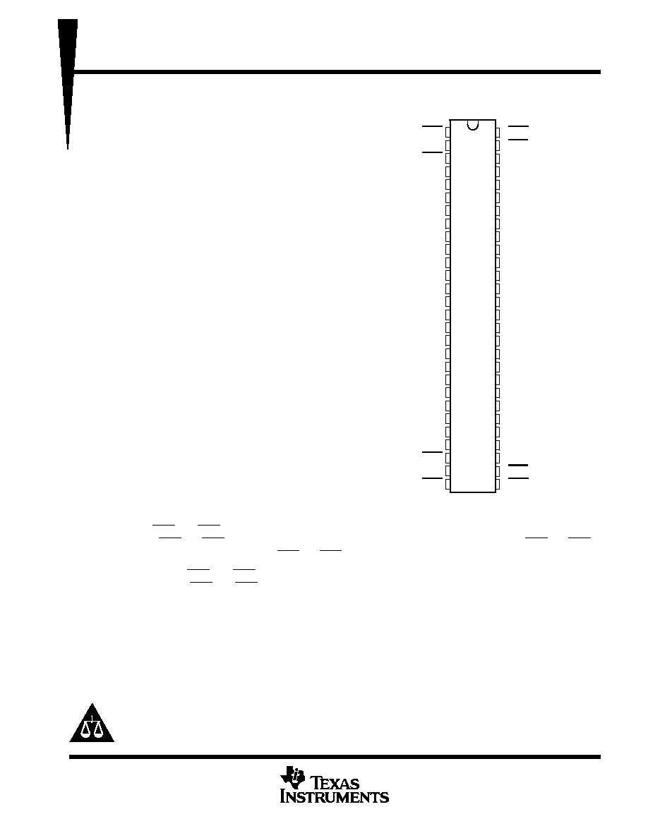
54ACT16833 . . . WD PACKAGE
74ACT16833 . . . DL PACKAGE
(TOP VIEW)
1
2
3
4
5
6
7
8
9
10
11
12
13
14
15
16
17
18
19
20
21
22
23
24
25
26
27
28
56
55
54
53
52
51
50
49
48
47
46
45
44
43
42
41
40
39
38
37
36
35
34
33
32
31
30
29
1OEB
1CLK
1ERR
GND
1A1
1A2
V
CC
1A3
1A4
1A5
GND
1A6
1A7
1A8
2A1
2A2
2A3
GND
2A4
2A5
2A6
V
CC
2A7
2A8
GND
2ERR
2CLK
2OEB
1OEA
1CLR
1PARITY
GND
1B1
1B2
V
CC
1B3
1B4
1B5
GND
1B6
1B7
1B8
2B1
2B2
2B3
GND
2B4
2B5
2B6
V
CC
2B7
2B8
GND
2PARITY
2CLR
2OEA
54ACT16833, 74ACT16833
DUAL 8-BIT TO 9-BIT PARITY BUS TRANSCEIVERS
SCAS166A ≠ JUNE 1990 ≠ REVISED APRIL 1996
2
POST OFFICE BOX 655303
∑
DALLAS, TEXAS 75265
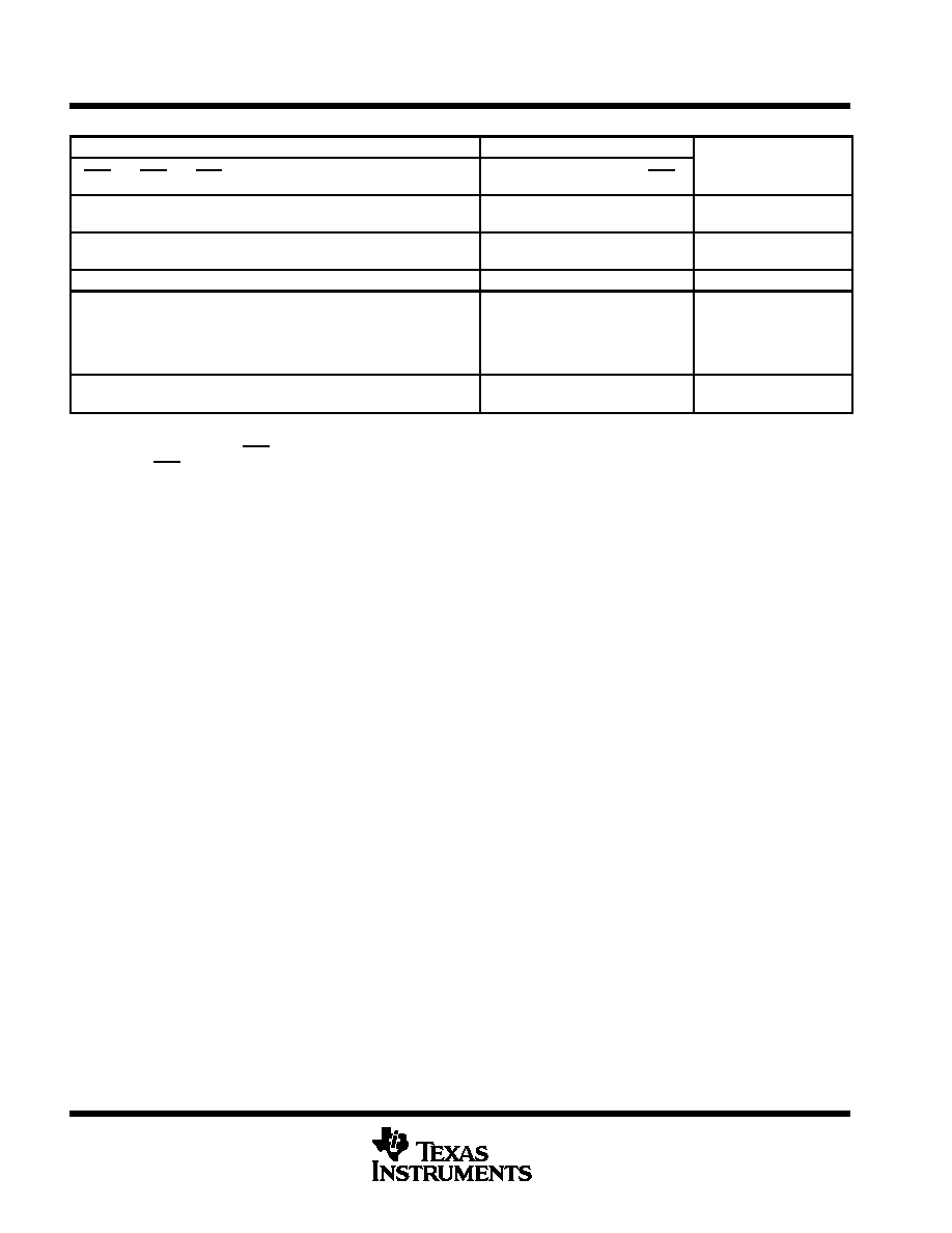
FUNCTION TABLE
INPUTS
OUTPUT AND I/O
OEB
OEA
CLR
CLK
Ai
OF H
Bi
OF H
A
B
PARITY
ERR
FUNCTION
L
H
X
X
Odd
Even
NA
NA
A
L
H
NA
A data to B bus and
generate parity
H
L
H
NA
Odd
Even
B
NA
NA
H
L
B data to A bus and
check parity
X
X
L
X
X
X
X
NA
NA
H
Check error-flag register
H
No
X
NC
ß
H
H
L
No
X
X
Z
Z
Z
H
Isolationß
H
H
H
Odd
X
Z
Z
Z
H
Isolationß
H
Even
L
L
L
X
X
Odd
Even
NA
NA
A
H
L
NA
A data to B bus and
generate inverted parity
NA = not applicable, NC = no change, X = don't care
Summation of high-level inputs includes PARITY along with Bi inputs.
Output states shown assume ERR was previously high.
ß In this mode, ERR (when clocked) shows inverted parity of the A bus.

54ACT16833, 74ACT16833
DUAL 8-BIT TO 9-BIT PARITY BUS TRANSCEIVERS
SCAS166A ≠ JUNE 1990 ≠ REVISED APRIL 1996
3
POST OFFICE BOX 655303
∑
DALLAS, TEXAS 75265
logic symbol
1ERR
1CLR
1OEA
1OEB
PARITY XCVR
1CLR
55
1CLK
2
1CLK
1
5
1A1
6
1A2
8
1A3
9
1A4
3
1PARITY
54
1PARITY
1B5
47
1B6
45
1B7
44
1B8
43
8
1OEA
56
1OEB
1
10
1A5
12
1A6
13
1A7
8
14
1A8
1B1
52
1
1B2
51
1B3
49
1B4
48
1ERR
'ACT16833
2CLR
30
2CLK
27
2CLK
26
2PARITY
31
2PARITY
2OEA
29
2OEB
28
2ERR
2CLR
2OEA
2OEB
2ERR
1
15
2A1
16
2A2
17
2A3
19
2A4
2B5
37
2B6
36
2B7
34
2B8
33
8
20
2A5
21
2A6
23
2A7
8
24
2A8
2B1
42
1
2B2
41
2B3
40
2B4
38
This symbol is in accordance with ANSI/IEEE Std 91-1984 and IEC Publication 617-12.
A Bus
B Bus
A Bus
B Bus

54ACT16833, 74ACT16833
DUAL 8-BIT TO 9-BIT PARITY BUS TRANSCEIVERS
SCAS166A ≠ JUNE 1990 ≠ REVISED APRIL 1996
4
POST OFFICE BOX 655303
∑
DALLAS, TEXAS 75265
logic diagram (positive logic)
1ERR
1CLR
1OEA
1OEB
8
8
8
8
8
9
P
MUX
1
1
1
G1
1
2k
1D
R
C1
EN
EN
8 x
8 x
1A1≠1A8
1CLK
1PARITY
1B1≠1B8
2ERR
2CLR
2OEA
2OEB
8
8
8
8
8
9
P
MUX
1
1
1
G1
1
2k
1D
R
C1
EN
EN
8 x
8 x
2A1≠2A8
2CLK
2PARITY
2B1≠2B8
1
56
2
55
28
29
27
30
54
3
31
26

54ACT16833, 74ACT16833
DUAL 8-BIT TO 9-BIT PARITY BUS TRANSCEIVERS
SCAS166A ≠ JUNE 1990 ≠ REVISED APRIL 1996
5
POST OFFICE BOX 655303
∑
DALLAS, TEXAS 75265
ERROR FLAG FUNCTION TABLE
INPUTS
INTERNAL
TO DEVICE
OUTPUT
PRE-STATE
OUTPUT
ERR
FUNCTION
CLR
CLK
POINT P
ERRn ≠ 1
ERR
H
H
H
H
H
X
L
L
Sample
H
L
X
L
L
X
X
X
H
Clear
The state of ERR before any changes at CLR, CLK, or point P
Location of point P is shown on local diagram.
timing waveforms, error flag
ERR
CLR
CLK
OEA
OEB
tPLH
tPHL
tsu
tw
tw
tsu
th
Bi + PARITY
H
L
H
L
Even
Odd
H
L
H
L
H
L
absolute maximum ratings over operating free-air temperature range (unless otherwise noted)
ß
Supply voltage range, V
CC
≠0.5 V to 7 V
. . . . . . . . . . . . . . . . . . . . . . . . . . . . . . . . . . . . . . . . . . . . . . . . . . . . . . . . . .
Input voltage range, V
I
(see Note 1)
≠0.5 V to V
CC
+ 0.5 V
. . . . . . . . . . . . . . . . . . . . . . . . . . . . . . . . . . . . . . . . . . .
Output voltage range, V
O
(see Note 1)
≠0.5 V to V
CC
+ 0.5 V
. . . . . . . . . . . . . . . . . . . . . . . . . . . . . . . . . . . . . . . .
Input clamp current, I
IK
(V
I
< 0 or V
I
> V
CC
)
±
20 mA
. . . . . . . . . . . . . . . . . . . . . . . . . . . . . . . . . . . . . . . . . . . . . . . .
Output clamp current, I
OK
(V
O
< 0 or V
O
> V
CC
)
±
50 mA
. . . . . . . . . . . . . . . . . . . . . . . . . . . . . . . . . . . . . . . . . . . .
Continuous output current, I
O
(V
O
= 0 to V
CC
)
±
50 mA
. . . . . . . . . . . . . . . . . . . . . . . . . . . . . . . . . . . . . . . . . . . . . .
Continuous current through V
CC
or GND
±
450 mA
. . . . . . . . . . . . . . . . . . . . . . . . . . . . . . . . . . . . . . . . . . . . . . . . . .
Maximum power package dissipation at T
A
= 55
∞
C (in still air) (see Note 2): DL package
1.4 W
. . . . . . . . . . .
Storage temperature range, T
stg
≠65
∞
C to 150
∞
C
. . . . . . . . . . . . . . . . . . . . . . . . . . . . . . . . . . . . . . . . . . . . . . . . . . .
ß Stresses beyond those listed under "absolute maximum ratings" may cause permanent damage to the device. These are stress ratings only, and
functional operation of the device at these or any other conditions beyond those indicated under "recommended operating conditions" is not
implied. Exposure to absolute-maximum-rated conditions for extended periods may affect device reliability.
NOTES:
1. The input and output voltage ratings may be exceeded if the input and output current ratings are observed.
2. The maximum package power dissipation is calculated using a junction temperature of 150
∞
C and a board trace length of 750 mils.