LM124, LM124A, LM224, LM224A
LM324, LM324A, LM324K, LM324KA, LM2902
QUADRUPLE OPERATIONAL AMPLIFIERS
SLOS066J - SEPTEMBER 1975 - REVISED SEPTEMBER 2003
1
POST OFFICE BOX 655303
∑
DALLAS, TEXAS 75265
D
2-kV HBM ESD Protection (LM324K,
LM324KA)
D
Wide Range of Supply Voltages:
Single Supply . . . 3 V to 30 V
(LM2902, 3 V to 26 V) or Dual Supplies
D
Low Supply-Current Drain Independent of
Supply Voltage . . . 0.8 mA Typ
D
Common-Mode Input Voltage Range
Includes Ground, Allowing Direct Sensing
Near Ground
D
Low Input Bias and Offset Parameters:
- Input Offset Voltage . . . 3 mV Typ
A Versions . . . 2 mV Typ
- Input Offset Current . . . 2 nA Typ
- Input Bias Current . . . 20 nA Typ
A Versions . . . 15 nA Typ
D
Differential Input Voltage Range Equal to
Maximum-Rated Supply Voltage . . . 32 V
(26 V for LM2902)
D
Open-Loop Differential Voltage
Amplification . . . 100 V/mV Typ
D
Internal Frequency Compensation
description/ordering information
These devices consist of four independent
high-gain frequency-compensated operational
amplifiers that are designed specifically to operate
from a single supply over a wide range of voltages.
Operation from split supplies also is possible
when the difference between the two supplies is
3 V to 30 V (for the LM2902, 3 V to 26 V) and V
CC
is at least 1.5 V more positive than the input
common-mode voltage. The low supply-current
drain is independent of the magnitude of the
supply voltage.
Applications include transducer amplifiers, dc amplification blocks, and all the conventional
operational-amplifier circuits that now can be more easily implemented in single-supply-voltage systems. For
example, the LM124 can be operated directly from the standard 5-V supply that is used in digital systems and
easily provides the required interface electronics without requiring additional
±
15-V supplies.
Copyright
2003, Texas Instruments Incorporated
PRODUCTION DATA information is current as of publication date.
Products conform to specifications per the terms of Texas Instruments
standard warranty. Production processing does not necessarily include
testing of all parameters.
1
2
3
4
5
6
7
14
13
12
11
10
9
8
1OUT
1IN-
1IN+
V
CC
2IN+
2IN-
2OUT
4OUT
4IN-
4IN+
GND
3IN+
3IN-
3OUT
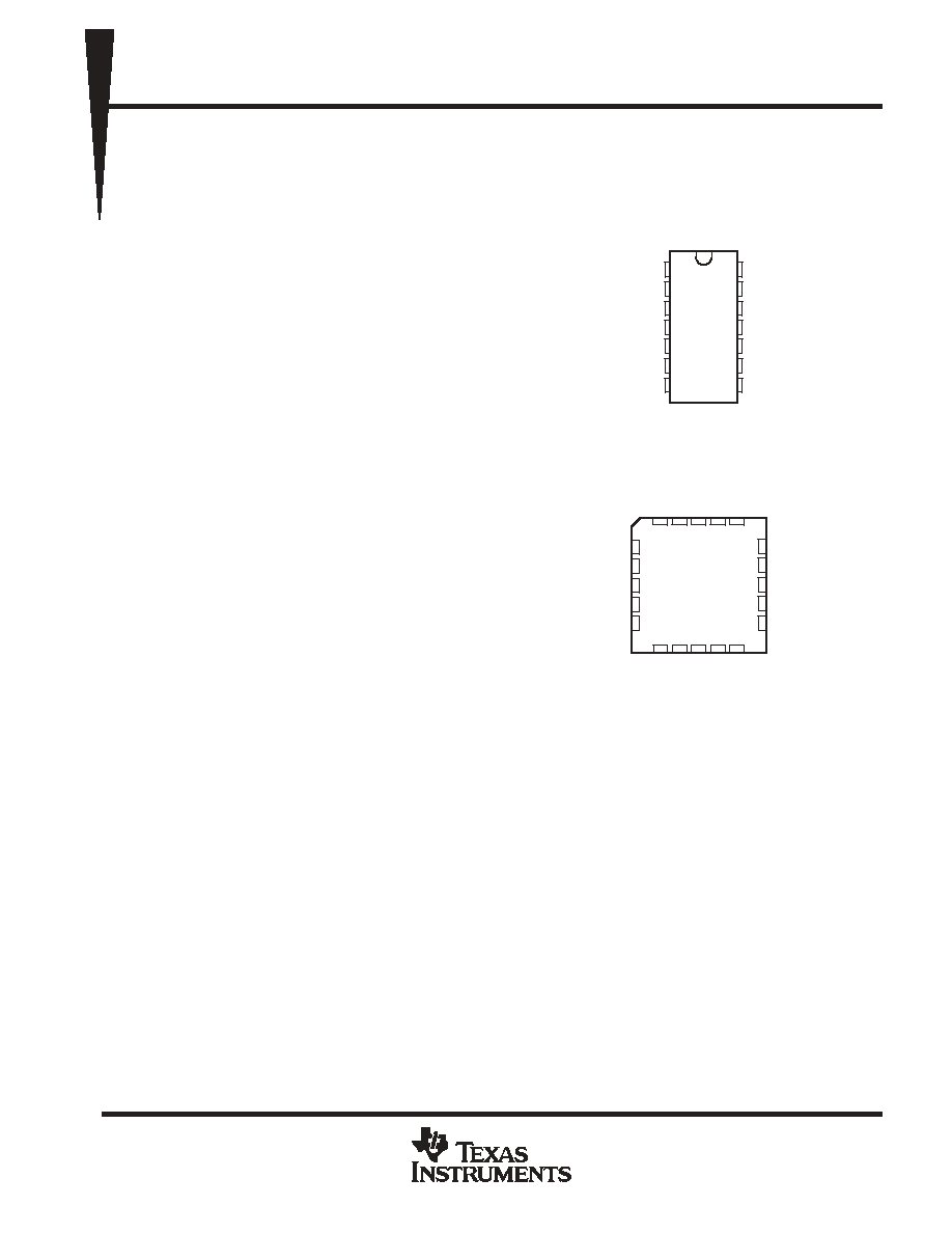
LM124 . . . D, J, OR W PACKAGE
LM124A . . . J PACKAGE
LM224, LM224A . . . D OR N PACKAGE
LM324, LM324K . . . D, N, NS, OR PW PACKAGE
LM324A . . . D, DB, N, NS, OR PW PACKAGE
LM324KA . . . D, N, NS, OR PW PACKAGE
LM2902 . . . D, N, NS, OR PW PACKAGE
(TOP VIEW)
3
2
1 20 19
9 10 11 12 13
4
5
6
7
8
18
17
16
15
14
4IN+
NC
GND
NC
3IN+
1IN+
NC
V
CC
NC
2IN+
LM124, LM124A . . . FK PACKAGE
(TOP VIEW)
1IN-
1OUT
NC
3IN-
4IN-
2IN-
2OUT
NC
NC - No internal connection
3OUT
4OUT
On products compliant to MIL PRF 38535, all parameters are tested
unless otherwise noted. On all other products, production
processing does not necessarily include testing of all parameters.
LM124, LM124A, LM224, LM224A
LM324, LM324A, LM324K, LM324KA, LM2902
QUADRUPLE OPERATIONAL AMPLIFIERS
SLOS066J - SEPTEMBER 1975 - REVISED SEPTEMBER 2003
2
POST OFFICE BOX 655303
∑
DALLAS, TEXAS 75265
description/ordering information (continued)
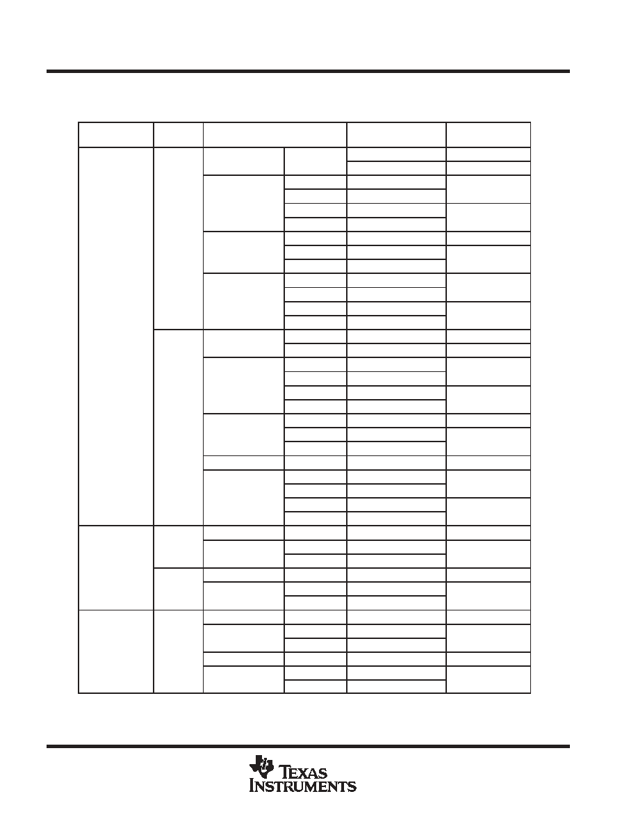
ORDERING INFORMATION
TA
VIOmax
AT 25
∞
C
PACKAGE
ORDERABLE
PART NUMBER
TOP-SIDE
MARKING
PDIP (N)
Tube of 25
LM324N
LM324N
PDIP (N)
Tube of 25
LM324KN
LM324KN
Tube of 50
LM324D
LM324
SOIC (D)
Reel of 2500
LM324DR
LM324
SOIC (D)
Tube of 50
LM324KD
LM324K
Reel of 2500
LM324KDR
LM324K
7 mV
Reel of 2000
LM324NSR
LM324
7 mV
SOP (NS)
Tube of 50
LM324KNS
LM324K
SOP (NS)
Reel of 2000
LM324KNSR
LM324K
Tube of 90
LM324PW
L324
TSSOP (PW)
Reel of 2000
LM324PWR
L324
TSSOP (PW)
Tube of 90
LM324KPW
L324K
Reel of 2000
LM324KPWR
L324K
0
∞
C to 70
∞
C
PDIP (N)
Tube of 25
LM324AN
LM324AN
0 C to 70 C
PDIP (N)
Tube of 25
LM324KAN
LM324KAN
Tube of 50
LM324AD
LM324A
SOIC (D)
Reel of 2500
LM324ADR
LM324A
SOIC (D)
Tube of 50
LM324KAD
LM324KA
Reel of 2500
LM324KADR
LM324KA
3 mV
Reel of 2000
LM324ANSR
LM324A
3 mV
SOP (NS)
Tube of 50
LM324KANS
LM324KA
SOP (NS)
Reel of 2000
LM324KANSR
LM324KA
SSOP (DB)
Reel of 2000
LM324ADBR
LM324A
Tube of 90
LM324APW
L324A
TSSOP (PW)
Reel of 2000
LM324APWR
L324A
TSSOP (PW)
Tube of 90
LM324KAPW
L324KA
Reel of 2000
LM324KAPWR
L324KA
PDIP (N)
Tube of 25
LM224N
LM224N
5 mV
SOIC (D)
Tube of 50
LM224D
LM224
-25
∞
C to 85
∞
C
5 mV
SOIC (D)
Reel of 2500
LM224DR
LM224
-25
∞
C to 85
∞
C
PDIP (N)
Tube of 25
LM224AN
LM224AN
3 mV
SOIC (D)
Tube of 50
LM224AD
LM224A
3 mV
SOIC (D)
Reel of 2500
LM224ADR
LM224A
PDIP (N)
Tube of 25
LM2902N
LM2902N
SOIC (D)
Tube of 50
LM2902D
LM2902
-40
∞
C to 125
∞
C
7 mV
SOIC (D)
Reel of 2500
LM2902DR
LM2902
-40
∞
C to 125
∞
C
7 mV
SOP (NS)
Reel of 2000
LM2902NSR
LM2902
TSSOP (PW)
Tube of 90
LM2902PW
L2902
TSSOP (PW)
Reel of 2000
LM2902PWR
L2902
Package drawings, standard packing quantities, thermal data, symbolization, and PCB design guidelines are available at
www.ti.com/sc/package.
LM124, LM124A, LM224, LM224A
LM324, LM324A, LM324K, LM324KA, LM2902
QUADRUPLE OPERATIONAL AMPLIFIERS
SLOS066J - SEPTEMBER 1975 - REVISED SEPTEMBER 2003
3
POST OFFICE BOX 655303
∑
DALLAS, TEXAS 75265
description/ordering information (continued)
ORDERING INFORMATION
TA
VIOmax
AT 25
∞
C
PACKAGE
ORDERABLE
PART NUMBER
TOP-SIDE
MARKING
CDIP (J)
Tube of 25
LM124J
LM124J
CFP (W)
Tube of 25
LM124W
LM124W
5 mV
LCCC (FK)
Tube of 55
LM124FK
LM124FK
-55
∞
C to 125
∞
C
5 mV
SOIC (D)
Tube of 50
LM124D
LM124
-55 C to 125 C
SOIC (D)
Reel of 2500
LM124DR
LM124
2 mV
CDIP (J)
Tube of 25
LM124AJ
LM124AJ
2 mV
LCCC (FK)
Tube of 55
LM124AFK
LM124AFK
Package drawings, standard packing quantities, thermal data, symbolization, and PCB design guidelines are available at
www.ti.com/sc/package.
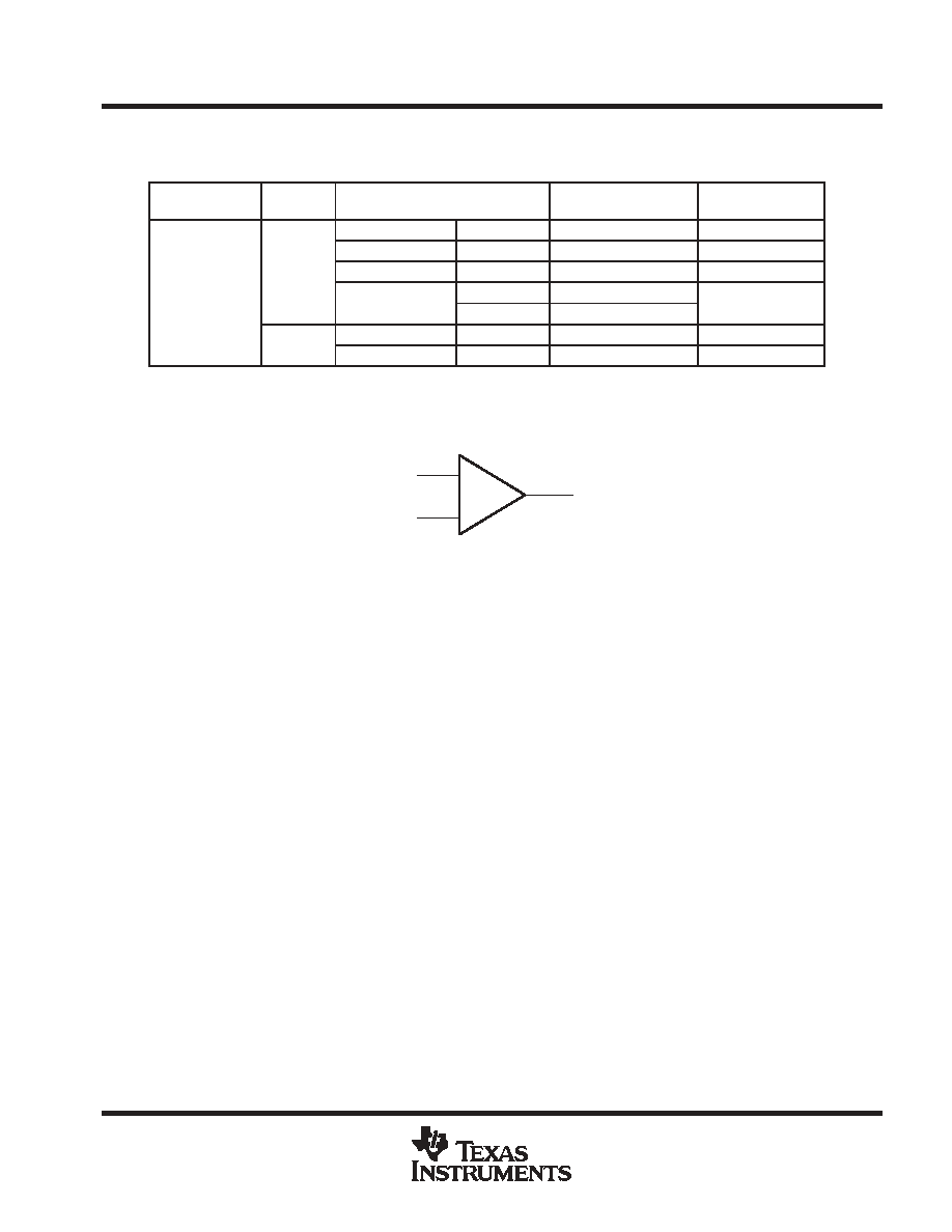
symbol (each amplifier)
-
+
IN-
IN+
OUT
LM124, LM124A, LM224, LM224A
LM324, LM324A, LM324K, LM324KA, LM2902
QUADRUPLE OPERATIONAL AMPLIFIERS
SLOS066J - SEPTEMBER 1975 - REVISED SEPTEMBER 2003
4
POST OFFICE BOX 655303
∑
DALLAS, TEXAS 75265
schematic (each amplifier)
To Other
Amplifiers
6-
µ
A
Current
Regulator
VCC
OUT
GND
IN-
IN+
100-
µ
A
Current
Regulator
50-
µ
A
Current
Regulator
COMPONENT COUNT
(total device)
Epi-FET
Transistors
Diodes
Resistors
Capacitors
1
95
4
11
4
6-
µ
A
Current
Regulator
LM124, LM124A, LM224, LM224A
LM324, LM324A, LM324K, LM324KA, LM2902
QUADRUPLE OPERATIONAL AMPLIFIERS
SLOS066J - SEPTEMBER 1975 - REVISED SEPTEMBER 2003
5
POST OFFICE BOX 655303
∑
DALLAS, TEXAS 75265
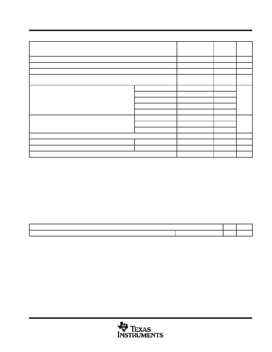
absolute maximum ratings over operating free-air temperature range (unless otherwise noted)
LM124, LM124A
LM224, LM224A
LM324, LM324A
LM2902
UNIT
Supply voltage, VCC (see Note 1)
±
16 or 32
±
13 or 26
V
Differential input voltage, VID (see Note 2)
±
32
±
26
V
Input voltage, VI (either input)
-0.3 to 32
-0.3 to 26
V
Duration of output short circuit (one amplifier) to ground at (or below) TA = 25
∞
C,
VCC
15 V (see Note 3)
Unlimited
Unlimited
D package
86
86
DB package
96
Package thermal impedance,
JA (see Notes 4 and 5)
N package
80
80
∞
C/W
Package thermal impedance,
JA (see Notes 4 and 5)
NS package
76
76
C/W
PW package
113
113
FK package
5.61
Package thermal impedance,
JC (see Notes 6 and 7)
J package
15.05
∞
C/W
Package thermal impedance,
JC (see Notes 6 and 7)
W package
14.65
C/W
Operating virtual junction temperature, TJ
150
150
∞
C
Case temperature for 60 seconds
FK package
260
∞
C
Lead temperature 1,6 mm (1/16 inch) from case for 60 seconds
J or W package
300
300
∞
C
Storage temperature range, Tstg
-65 to 150
-65 to 150
∞
C
Stresses beyond those listed under "absolute maximum ratings" may cause permanent damage to the device. These are stress ratings only, and
functional operation of the device at these or any other conditions beyond those indicated under "recommended operating conditions" is not
implied. Exposure to absolute-maximum-rated conditions for extended periods may affect device reliability.
NOTES:
1. All voltage values (except differential voltages and VCC specified for the measurement of IOS) are with respect to the network GND.
2. Differential voltages are at IN+ with respect to IN-.
3. Short circuits from outputs to VCC can cause excessive heating and eventual destruction.
4. Maximum power dissipation is a function of TJ(max),
JA, and TA. The maximum allowable power dissipation at any allowable
ambient temperature is PD = (TJ(max) - TA)/
JA. Operating at the absolute maximum TJ of 150
∞
C can affect reliability.
5. The package thermal impedance is calculated in accordance with JESD 51-7.
6. Maximum power dissipation is a function of TJ(max),
JC, and TC. The maximum allowable power dissipation at any allowable case
temperature is PD = (TJ(max) - TC)/
JC. Operating at the absolute maximum TJ of 150
∞
C can affect reliability.
7. The package thermal impedance is calculated in accordance with MIL-STD-883.
ESD protection
TEST CONDITION
TYP
UNIT
Human Body Model
LM324K, LM324KA
±
2
kV