UC1842/3/4/5
UC2842/3/4/5
UC3842/3/4/5
Current Mode PWM Controller
FEATURES
∑
Optimized For Off-line And DC
To DC Converters
∑
Low Start Up Current (<1mA)
∑
Automatic Feed Forward
Compensation
∑
Pulse-by-pulse Current Limiting
∑
Enhanced Load Response
Characteristics
∑
Under-voltage Lockout With
Hysteresis
∑
Double Pulse Suppression
∑
High Current Totem Pole
Output
∑
Internally Trimmed Bandgap
Reference
∑
500khz Operation
∑
Low R
O
Error Amp
DESCRIPTION
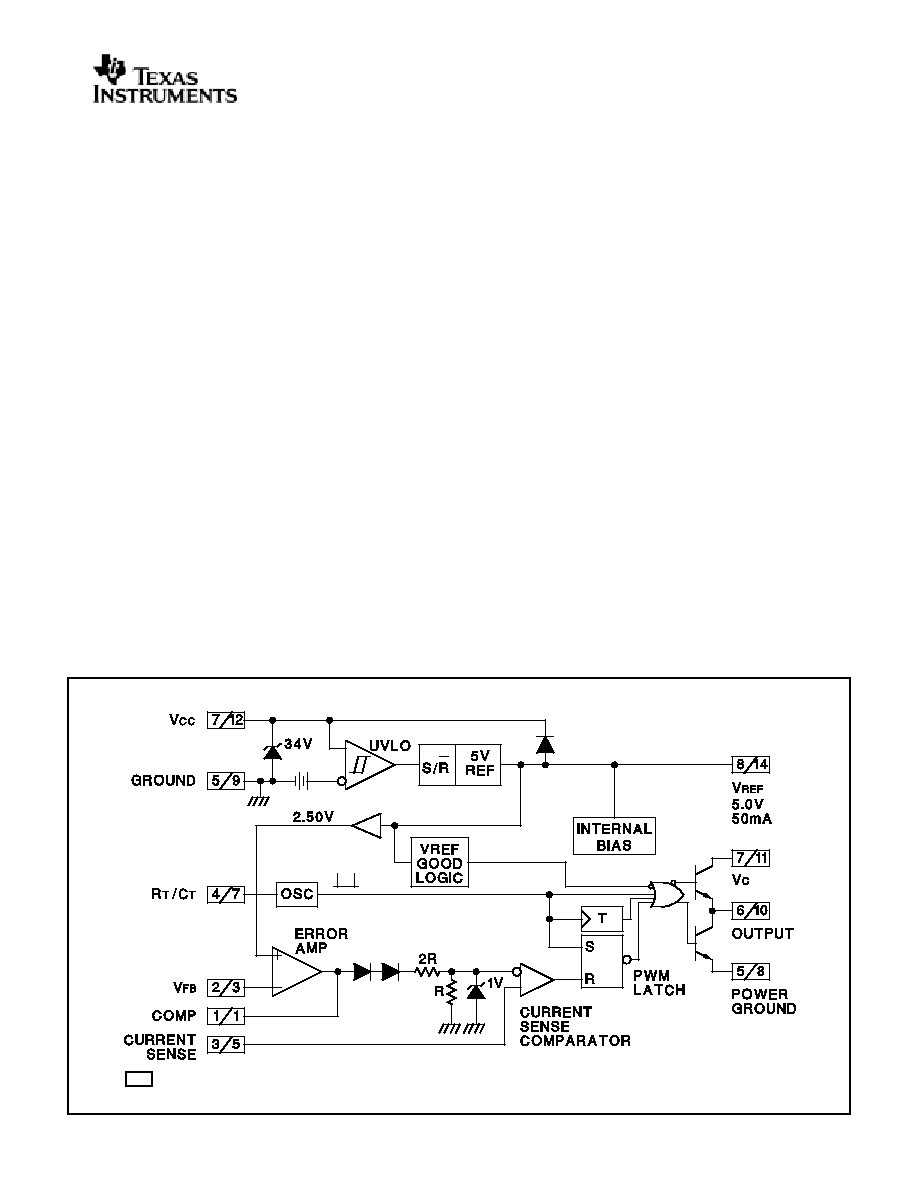
The UC1842/3/4/5 family of control ICs provides the necessary features to
implement off-line or DC to DC fixed frequency current mode control schemes
with a minimal external parts count. Internally implemented circuits include
under-voltage lockout featuring start up current less than 1mA, a precision
reference trimmed for accuracy at the error amp input, logic to insure latched
operation, a PWM comparator which also provides current limit control, and a
totem pole output stage designed to source or sink high peak current. The
output stage, suitable for driving N Channel MOSFETs, is low in the off state.
Differences between members of this family are the under-voltage lockout
thresholds and maximum duty cycle ranges. The UC1842 and UC1844 have
UVLO thresholds of 16V (on) and 10V (off), ideally suited to off-line
applications. The corresponding thresholds for the UC1843 and UC1845 are
8.4V and 7.6V. The UC1842 and UC1843 can operate to duty cycles
approaching 100%. A range of zero to 50% is obtained by the UC1844 and
UC1845 by the addition of an internal toggle flip flop which blanks the output
off every other clock cycle.
BLOCK DIAGRAM
A/B
Note 1:
A = DIL-8 Pin Number. B = SO-14 and CFP-14 Pin Number.
Note 2:
Toggle flip flop used only in 1844 and 1845.
SLUS223A - APRIL 1997 - REVISED MAY 2002
2
UC1842/3/4/5
UC2842/3/4/5
UC3842/3/4/5
ABSOLUTE MAXIMUM RATINGS(Note 1)
Supply Voltage (Low Impedance Source) . . . . . . . . . . . . . . 30V
Supply Voltage (I
CC
< 30mA) . . . . . . . . . . . . . . . . . Self Limiting
Output Current. . . . . . . . . . . . . . . . . . . . . . . . . . . . . . . . . . .
±
1A
Output Energy (Capacitive Load) . . . . . . . . . . . . . . . . . . . . 5
µ
J
Analog Inputs (Pins 2, 3). . . . . . . . . . . . . . . . . . . -0.3V to +6.3V
Error Amp Output Sink Current . . . . . . . . . . . . . . . . . . . . 10 mA
Power Dissipation at T
A
25
∞
C
(
DIL
-8) . . . . . . . . . . . . . . . . .
1 W
Power Dissipation at T
A
25∞C (SOIC-14) . . . . . . . . . 725 mW
Storage Temperature Range . . . . . . . . . . . . . . -65∞C to +150∞C
Junction Temperature Range . . . . . . . . . . . . . -55∞C to +150∞C
Lead Temperature (soldering, 10 seconds) . . . . . . . . . . . 300∞C
Note 1:
All voltages are with respect to Pin 5.
All currents are positive into the specified terminal.
Consult Packaging Section of Databook for thermal
limitations and considerations of packages.
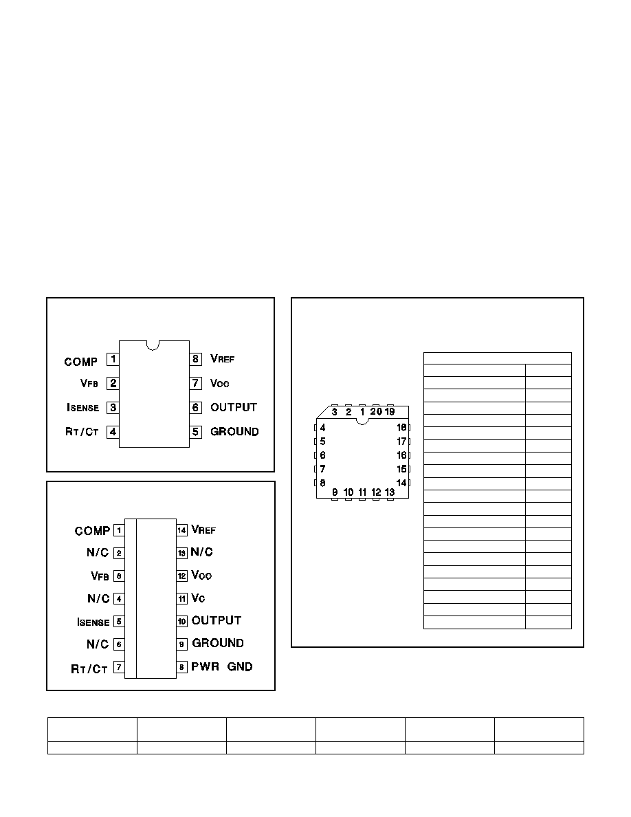
CONNECTION DIAGRAMS
DIL-8, SOIC-8 (TOP VIEW)
N or J Package, D8 Package
PLCC-20 (TOP VIEW)
Q Package
SOIC-14, CFP-14. (TOP VIEW)
D or W Package
PACKAGE PIN FUNCTION
FUNCTION
PIN
N/C
1
COMP
2
N/C
3
N/C
4
V
FB
5
N/C
6
I
SENSE
7
N/C
8
N/C
9
R
T
/C
T
10
N/C
11
PWR GND
12
GROUND
13
N/C
14
OUTPUT
15
N/C
16
V
C
17
V
CC
18
N/C
19
V
REF
20
Package
TA
25∞C
Power Rating
Derating Factor
Above TA
25∞C
TA
70∞C
Power Rating
TA
85∞C
Power Rating
TA
125∞C
Power Rating
W
700 mW
5.5 mW/∞C
452 mW
370 mW
150 mW
DISSIPATION RATING TABLE
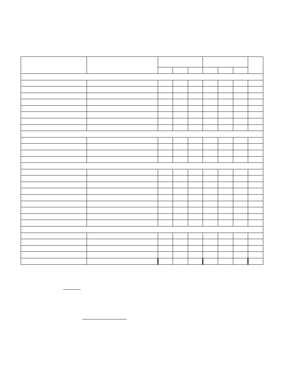
3
PARAMETER
TEST CONDITIONS
UC1842/3/4/5
UC2842/3/4/5
UC3842/3/4/5
UNITS
MIN
TYP
MAX
MIN
TYP
MAX
Reference Section
Output Voltage
T
J
= 25∞C, I
O
= 1mA
4.95
5.00
5.05
4.90
5.00
5.10
V
Line Regulation
12
V
IN
25V
6
20
6
20
mV
Load Regulation
1
I
0
20mA
6
25
6
25
mV
Temp. Stability
(Note 2) (Note 7)
0.2
0.4
0.2
0.4
mV/∞C
Total Output Variation
Line, Load, Temp. (Note 2)
4.9
5.1
4.82
5.18
V
Output Noise Voltage
10Hz
f
10kHz, T
J
= 25∞C (Note2)
50
50
µ
V
Long Term Stability
T
A
= 125∞C, 1000Hrs. (Note 2)
5
25
5
25
mV
Output Short Circuit
-30
-100
-180
-30
-100
-180
mA
Oscillator Section
Initial Accuracy
T
J
= 25∞C (Note 6)
47
52
57
47
52
57
kHz
Voltage Stability
12
V
CC
25V
0.2
1
0.2
1
%
Temp. Stability
T
MIN
T
A
T
MAX
(Note 2)
5
5
%
Amplitude
V
PIN 4
peak to peak (Note 2)
1.7
1.7
V
Error Amp Section
Input Voltage
V
PIN 1
= 2.5V
2.45
2.50
2.55
2.42
2.50
2.58
V
Input Bias Current
-0.3
-1
-0.3
-2
µ
A
A
VOL
2
V
O
4V
65
90
65
90
dB
Unity Gain Bandwidth
(Note 2) T
J
= 25∞C
0.7
1
0.7
1
MHz
PSRR
12
V
CC
25V
60
70
60
70
dB
Output Sink Current
V
PIN 2
= 2.7V, V
PIN 1
= 1.1V
2
6
2
6
mA
Output Source Current
V
PIN 2
= 2.3V, V
PIN 1
= 5V
-0.5
-0.8
-0.5
-0.8
mA
V
OUT
High
V
PIN 2
= 2.3V, R
L
= 15k to ground
5
6
5
6
V
V
OUT
Low
V
PIN 2
= 2.7V, R
L
= 15k to Pin 8
0.7
1.1
0.7
1.1
V
Current Sense Section
Gain
(Notes 3 and 4)
2.85
3
3.15
2.85
3
3.15
V/V
Maximum Input Signal
V
PIN 1
= 5V (Note 3)
0.9
1
1.1
0.9
1
1.1
V
PSRR
12
V
CC
25V (Note 3) (Note 2)
70
70
dB
Input Bias Current
-2
-10
-2
-10
µ
A
Delay to Output
V
PIN 3
= 0 to 2V (Note 2)
150
300
150
300
ns
UC1842/3/4/5
UC2842/3/4/5
UC3842/3/4/5
ELECTRICAL CHARACTERISTICS:
Unless otherwise stated, these specifications apply for -55∞C
T
A
125∞C for the
UC184X; -40∞C
T
A
85∞C for the UC284X; 0
∞
C
T
A
70∞C for the 384X; V
CC
= 15V
(Note 5); R
T
= 10k; C
T
= 3.3nF, T
A
=T
J.
Note 2:
These parameters, although guaranteed, are not 100% tested in production.
Note 3:
Parameter measured at trip point of latch with V
PIN 2
= 0.
Note 4:
Gain defined as
A
VPIN
VPIN
VPIN
V
=
1
3
0
3 0 8
,
.
Note 5:
Adjust V
CC
above the start threshold before setting at 15V.
Note 6:
Output frequency equals oscillator frequency for the UC1842 and UC1843.
Output frequency is one half oscillator frequency for the UC1844 and UC1845.
Note 7:
Temperature stability, sometimes referred to as average temperature coefficient, is described by the equation:
Temp Stability V
max
VREF min
TJ max
TJ min
REF
=
-
-
(
)
(
)
(
)
(
)
V
REF
(max) and V
REF
(min) are the maximum and minimum reference voltages measured over the appropriate
temperature range. Note that the extremes in voltage do not necessarily occur at the extremes in temperature.
4
PARAMETER
TEST CONDITION
UC1842/3/4/5
UC2842/3/4/5
UC3842/3/4/5
UNITS
MIN
TYP
MAX
MIN
TYP
MAX
Output Section
Output Low Level
I
SINK
= 20mA
0.1
0.4
0.1
0.4
V
I
SINK
= 200mA
1.5
2.2
1.5
2.2
V
Output High Level
I
SOURCE
= 20mA
13
13.5
13
13.5
V
I
SOURCE
= 200mA
12
13.5
12
13.5
V
Rise Time
T
J
= 25∞C, C
L
= 1nF (Note 2)
50
150
50
150
ns
Fall Time
T
J
= 25∞C, C
L
= 1nF (Note 2)
50
150
50
150
ns
Under-voltage Lockout Section
Start Threshold
X842/4
15
16
17
14.5
16
17.5
V
X843/5
7.8
8.4
9.0
7.8
8.4
9.0
V
Min. Operating Voltage
After Turn On
X842/4
9
10
11
8.5
10
11.5
V
X843/5
7.0
7.6
8.2
7.0
7.6
8.2
V
PWM Section
Maximum Duty Cycle
X842/3
95
97
100
95
97
100
%
X844/5
46
48
50
47
48
50
%
Minimum Duty Cycle
0
0
%
Total Standby Current
Start-Up Current
0.5
1
0.5
1
mA
Operating Supply Current
V
PIN 2
= V
PIN 3
= 0V
11
17
11
17
mA
V
CC
Zener Voltage
I
CC
= 25mA
30
34
30
34
V
Note 2:
These parameters, although guaranteed, are not 100% tested in production.
Note 3:
Parameter measured at trip point of latch with V
PIN 2
= 0
.
Note 4:
Gain defined as: A
VPIN
VPIN
VPIN
V
=
1
3
0
3 0 8
;
. .
Note 5:
Adjust V
CC
above the start threshold before setting at 15V.
Note 6:
Output frequency equals oscillator frequency for the UC1842 and UC1843.
Output frequency is one half oscillator frequency for the UC1844 and UC1845.
UC1842/3/4/5
UC2842/3/4/5
UC3842/3/4/5
ELECTRICAL CHARACTERISTICS:
Unless otherwise stated, these specifications apply for
-
55∞C
T
A
125∞C for the
UC184X;
-
40∞C
T
A
85∞C for the UC284X; 0
∞
C
T
A
70∞C for the 384X; V
CC
=
15V (Note 5); R
T
= 10k; C
T
= 3.3nF, T
A
=T
J.
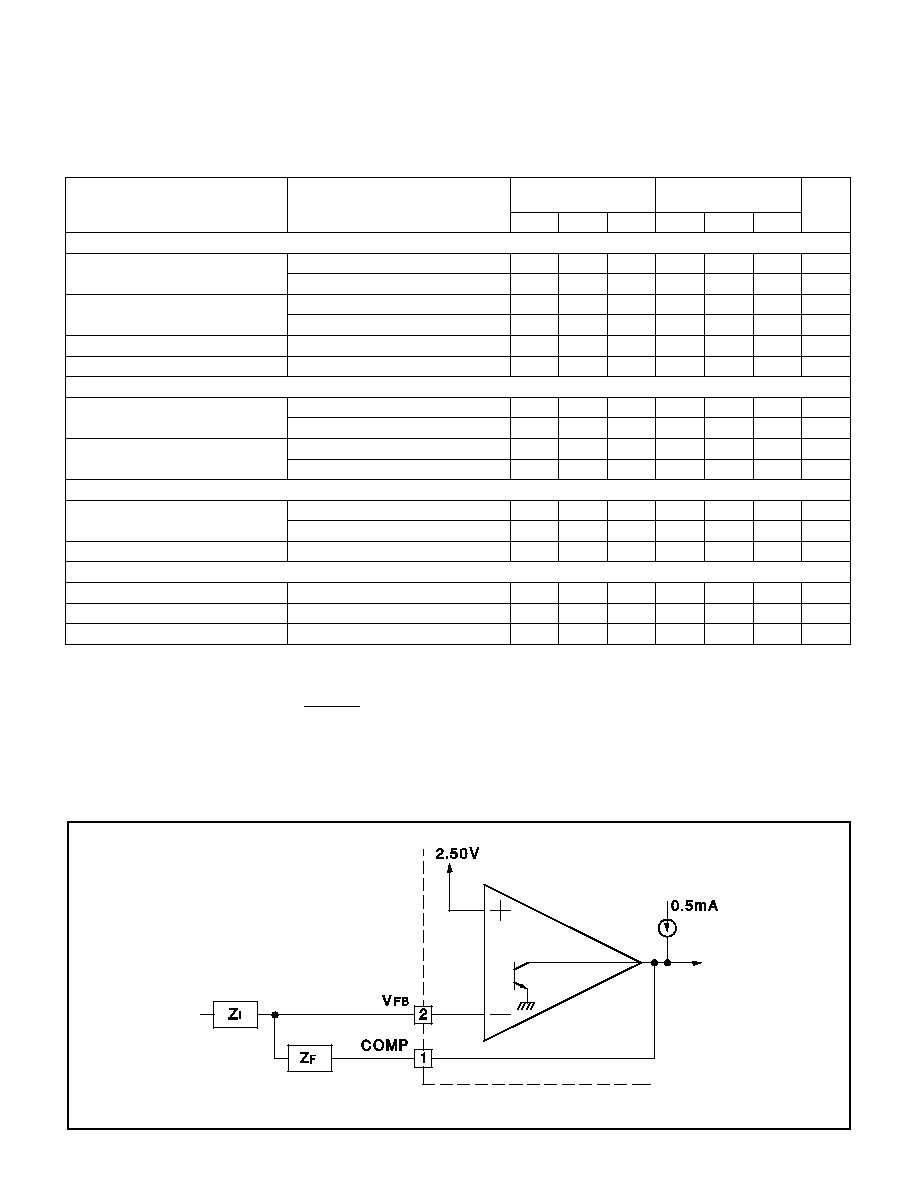
ERROR AMP CONFIGURATION
Error Amp can Source or Sink up to 0.5mA
5
UC1842/3/4/5
UC2842/3/4/5
UC3842/3/4/5
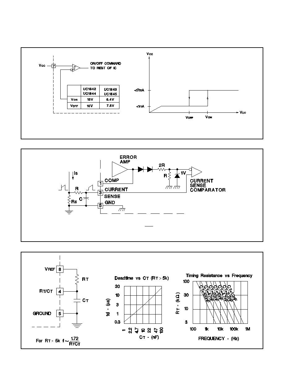
UNDER-VOLTAGE LOCKOUT
CURRENT SENSE CIRCUIT
OSCILLATOR SECTION
During under-voltage lock-out, the output driver is
biased to sink minor amounts of current. Pin 6 should
be shunted to ground with a bleeder resistor to prevent
activating the power switch with extraneous leakage
currents.
A small RC filter may be required to suppress switch transients
.
Peak Current (I
S
) is Determined By The Formula
I
SMAX
1.0V
RS