1
Data sheet acquired from Harris Semiconductor
SCHS158E
Features
∑ Three-State Buffered Outputs
∑ Gated Input and Output Enables
∑ Fanout (Over Temperature Range)
- Standard Outputs . . . . . . . . . . . . . . . 10 LSTTL Loads
- Bus Driver Outputs . . . . . . . . . . . . . 15 LSTTL Loads
∑ Wide Operating Temperature Range . . . -55
o
C to 125
o
C
∑ Balanced Propagation Delay and Transition Times
∑ Significant Power Reduction Compared to LSTTL
Logic ICs
∑ HC Types
- 2V to 6V Operation
- High Noise Immunity: N
IL
= 30%, N
IH
= 30% of V
CC
at V
CC
= 5V
∑ HCT Types
- 4.5V to 5.5V Operation
- Direct LSTTL Input Logic Compatibility,
V
IL
= 0.8V (Max), V
IH
= 2V (Min)
- CMOS Input Compatibility, I
l
1
µ
A at V
OL
, V
OH
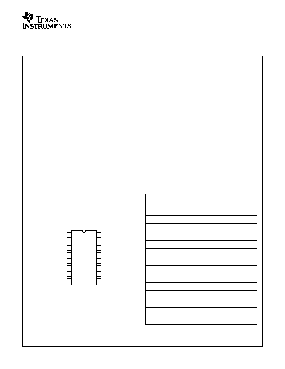
Pinout
CD54HC173, CD54HCT173
(CERDIP)
CD74HC173
(PDIP, SOIC, SOP, TSSOP)
CD74HCT173
(PDIP, SOIC)
TOP VIEW
Description
The 'HC173 and 'HCT173 high speed three-state quad D-
type flip-flops are fabricated with silicon gate CMOS technol-
ogy. They possess the low power consumption of standard
CMOS Integrated circuits, and can operate at speeds com-
parable to the equivalent low power Schottky devices. The
buffered outputs can drive 15 LSTTL loads. The large output
drive capability and three-state feature make these parts ide-
ally suited for interfacing with bus lines in bus oriented sys-
tems.
The four D-type flip-flops operate synchronously from a com-
mon clock. The outputs are in the three-state mode when
either of the two output disable pins are at the logic "1" level.
The input ENABLES allow the flip-flops to remain in their
present states without having to disrupt the clock If either of
the 2 input ENABLES are taken to a logic "1" level, the Q
outputs are fed back to the inputs, forcing the flip-flops to
remain in the same state. Reset is enabled by taking the
MASTER RESET (MR) input to a logic "1" level. The data
outputs change state on the positive going edge of the clock.
The 'HCT173 logic family is functionally, as well as pin com-
patible with the standard LS logic family
.
OE
OE2
Q
0
Q
1
Q
2
Q
3
GND
V
CC
MR
D0
D1
D2
D3
E2
14
15
16
9
13
12
11
10
1
2
3
4
5
7
6
8
E1
CP
Ordering Information
PART NUMBER
TEMP. RANGE
(
o
C)
PACKAGE
CD54HC173F3A
-55 to 125
16 Ld CERDIP
CD54HCT173F3A
-55 to 125
16 Ld CERDIP
CD74HC173E
-55 to 125
16 Ld PDIP
CD74HC173M
-55 to 125
16 Ld SOIC
CD74HC173MT
-55 to 125
16 Ld SOIC
CD74HC173M96
-55 to 125
16 Ld SOIC
CD74HC173NSR
-55 to 125
16 Ld SOP
CD74HC173PW
-55 to 125
16 Ld TSSOP
CD74HC173PWR
-55 to 125
16 Ld TSSOP
CD74HC173PWT
-55 to 125
16 Ld TSSOP
CD74HCT173E
-55 to 125
16 Ld PDIP
CD74HCT173M
-55 to 125
16 Ld SOIC
CD74HCT173MT
-55 to 125
16 Ld SOIC
CD74HCT173M96
-55 to 125
16 Ld SOIC
NOTE: When ordering, use the entire part number. The suffixes 96
and R denote tape and reel. The suffix T denotes a small-quantity
reel of 250.
February 1998 - Revised October 2003
CAUTION: These devices are sensitive to electrostatic discharge. Users should follow proper IC Handling Procedures.
Copyright
©
2003, Texas Instruments Incorporated
CD54HC173, CD74HC173,
CD54HCT173, CD74HCT173
High-Speed CMOS Logic
Quad D-Type Flip-Flop, Three-State
[ /Title
(CD74H
C173,
CD74H
CT173)
/Subject
(High
Speed
CMOS
Logic
Quad D-
Type
2
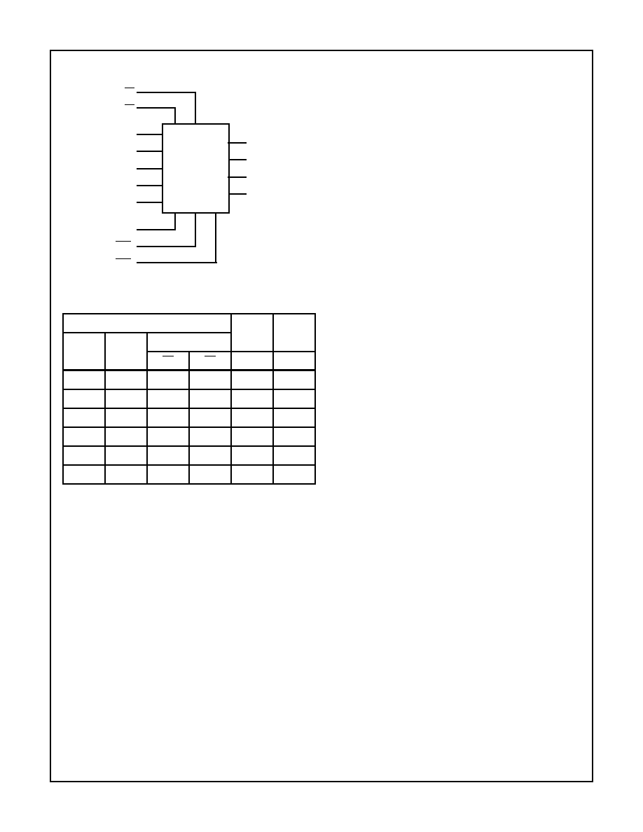
Functional Diagram
TRUTH TABLE
INPUTS
DATA
OUTPUT
MR
CP
DATA ENABLE
E1
E2
D
Q
n
H
X
X
X
X
L
L
L
X
X
X
Q
0
L
H
X
X
Q
0
L
X
H
X
Q
0
L
L
L
L
L
L
L
L
H
H
H= High Voltage Level
L = Low Voltage Level
X= Irrelevant
= Transition from Low to High Level
Q
0
= Level Before the Indicated Steady-State Input Conditions Were
Established
NOTE:
1. When either OE1 or OE2 (or both) is (are) high, the output is dis-
abled to the high-impedance state, however, sequential opera-
tion of the flip-flops is not affected.
3
4
Q
0
10
13
14
D1
D0
E2
E1
12
D2
11
D3
7
CP
OE1
2
MR
OE2
1
15
9
5
6
Q
3
Q
2
Q
1
CD54HC173, CD74HC173, CD54HCT173, CD74HCT173

3
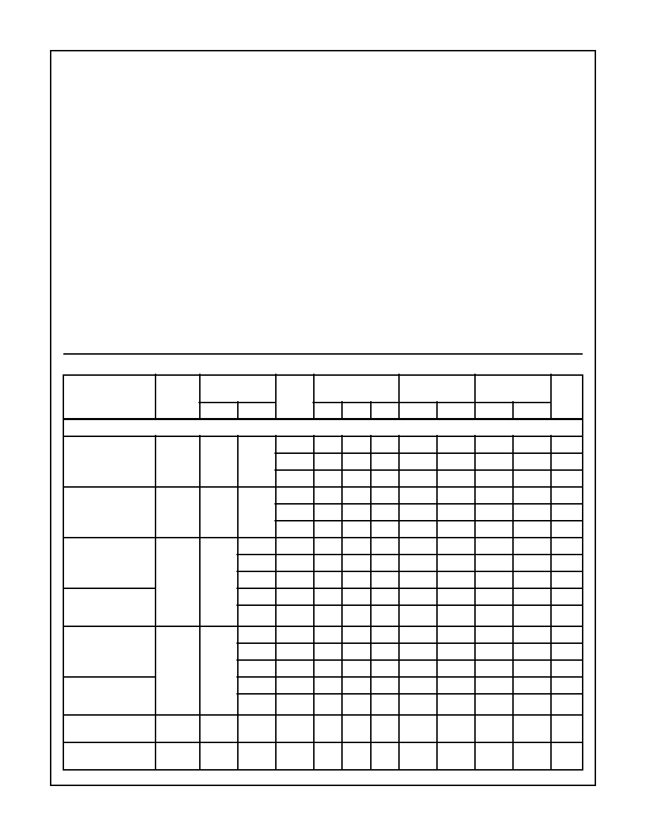
Logic Diagram
E1
E2
9
10
D0
CP
14
7
D
Q
CP
Q
R
MR
15
OE1
OE2
1
2
3 CIRCUITS IDENTICAL TO ABOVE CIRCUIT
IN DASHED ENCLOSURE
P
N
3
Q
0
13
12
11
D1
D2
D3
4
5
6
Q
1
Q
2
Q
3
V
CC
CD54HC173, CD74HC173, CD54HCT173, CD74HCT173
4
Absolute Maximum Ratings
Thermal Information
DC Supply Voltage, V
CC
. . . . . . . . . . . . . . . . . . . . . . . . -0.5V to 7V
DC Input Diode Current, I
IK
For V
I
< -0.5V or V
I
> V
CC
+ 0.5V
. . . . . . . . . . . . . . . . . . . . . .±
20mA
DC Output Diode Current, I
OK
For V
O
< -0.5V or V
O
> V
CC
+ 0.5V
. . . . . . . . . . . . . . . . . . . .±
20mA
DC Output Source or Sink Current per Output Pin, I
O
For V
O
> -0.5V or V
O
< V
CC
+ 0.5V
. . . . . . . . . . . . . . . . . . . .±
25mA
DC V
CC
or Ground Current, I
CC
. . . . . . . . . . . . . . . . . . . . . . . . .±
70mA
Operating Conditions
Temperature Range (T
A
) . . . . . . . . . . . . . . . . . . . . . -55
o
C to 125
o
C
Supply Voltage Range, V
CC
HC Types . . . . . . . . . . . . . . . . . . . . . . . . . . . . . . . . . . . . .2V to 6V
HCT Types . . . . . . . . . . . . . . . . . . . . . . . . . . . . . . . . .4.5V to 5.5V
DC Input or Output Voltage, V
I
, V
O
. . . . . . . . . . . . . . . . . 0V to V
CC
Input Rise and Fall Time
2V . . . . . . . . . . . . . . . . . . . . . . . . . . . . . . . . . . . . . . 1000ns (Max)
4.5V. . . . . . . . . . . . . . . . . . . . . . . . . . . . . . . . . . . . . . 500ns (Max)
6V . . . . . . . . . . . . . . . . . . . . . . . . . . . . . . . . . . . . . . . 400ns (Max)
Package Thermal Impedance,
JA
(see Note 2):
E (PDIP) Package . . . . . . . . . . . . . . . . . . . . . . . . . . . . . . . 67
o
C/W
M (SOIC) Package. . . . . . . . . . . . . . . . . . . . . . . . . . . . . . . 73
o
C/W
NS (SOP) Package . . . . . . . . . . . . . . . . . . . . . . . . . . . . . 64
C/W
PW (TSSOP) Package . . . . . . . . . . . . . . . . . . . . . . . . . 108
o
C/W
Maximum Junction Temperature . . . . . . . . . . . . . . . . . . . . . . . 150
o
C
Maximum Storage Temperature Range . . . . . . . . . .-65
o
C to 150
o
C
Maximum Lead Temperature (Soldering 10s) . . . . . . . . . . . . . 300
o
C
(SOIC - Lead Tips Only)
CAUTION: Stresses above those listed in "Absolute Maximum Ratings" may cause permanent damage to the device. This is a stress only rating and operation
of the device at these or any other conditions above those indicated in the operational sections of this specification is not implied.
NOTE:
2. The package thermal impedance is calculated in accordance with JESD 51-7.
DC Electrical Specifications
PARAMETER
SYMBOL
TEST
CONDITIONS
V
CC
(V)
25
o
C
-40
o
C TO 85
o
C
-55
o
C TO 125
o
C
UNITS
V
I
(V)
I
O
(mA)
MIN
TYP
MAX
MIN
MAX
MIN
MAX
HC TYPES
High Level Input
Voltage
V
IH
-
-
2
1.5
-
-
1.5
-
1.5
-
V
4.5
3.15
-
-
3.15
-
3.15
-
V
6
4.2
-
-
4.2
-
4.2
-
V
Low Level Input
Voltage
V
IL
-
-
2
-
-
0.5
-
0.5
-
0.5
V
4.5
-
-
1.35
-
1.35
-
1.35
V
6
-
-
1.8
-
1.8
-
1.8
V
High Level Output
Voltage
CMOS Loads
V
OH
V
IH
or
V
IL
-0.02
2
1.9
-
-
1.9
-
1.9
-
V
-0.02
4.5
4.4
-
-
4.4
-
4.4
-
V
-0.02
6
5.9
-
-
5.9
-
5.9
-
V
High Level Output
Voltage
TTL Loads
-6
4.5
3.98
-
-
3.84
-
3.7
-
V
-7.8
6
5.48
-
-
5.34
-
5.2
-
V
Low Level Output
Voltage
CMOS Loads
V
OL
V
IH
or
V
IL
0.02
2
-
-
0.1
-
0.1
-
0.1
V
0.02
4.5
-
-
0.1
-
0.1
-
0.1
V
0.02
6
-
-
0.1
-
0.1
-
0.1
V
Low Level Output
Voltage
TTL Loads
6
4.5
-
-
0.26
-
0.33
-
0.4
V
7.8
6
-
-
0.26
-
0.33
-
0.4
V
Input Leakage
Current
I
I
V
CC
or
GND
-
6
-
-
±
0.1
-
±
1
-
±
1
µ
A
Quiescent Device
Current
I
CC
V
CC
or
GND
0
6
-
-
8
-
80
-
160
µ
A
CD54HC173, CD74HC173, CD54HCT173, CD74HCT173
5
Three-State Leakage
Current
I
OZ
V
IL
or
V
IH
-
6
-
-
±
0.5
-
±
0.5
-
±
10
µ
A
HCT TYPES
High Level Input
Voltage
V
IH
-
-
4.5 to
5.5
2
-
-
2
-
2
-
V
Low Level Input
Voltage
V
IL
-
-
4.5 to
5.5
-
-
0.8
-
0.8
-
0.8
V
High Level Output
Voltage
CMOS Loads
V
OH
V
IH
or
V
IL
-0.02
4.5
4.4
-
-
4.4
-
4.4
-
V
High Level Output
Voltage
TTL Loads
-6
4.5
3.98
-
-
3.84
-
3.7
-
V
Low Level Output
Voltage
CMOS Loads
V
OL
V
IH
or
V
IL
0.02
4.5
-
-
0.1
-
0.1
-
0.1
V
Low Level Output
Voltage
TTL Loads
6
4.5
-
-
0.26
-
0.33
-
0.4
V
Input Leakage
Current
I
I
V
CC
to
GND
0
5.5
-
-
±
0.1
-
±
1
-
±
1
µ
A
Quiescent Device
Current
I
CC
V
CC
or
GND
0
5.5
-
-
8
-
80
-
160
µ
A
Additional Quiescent
Device Current Per
Input Pin: 1 Unit Load
I
CC
(Note 3)
V
CC
-2.1
-
4.5 to
5.5
-
100
360
-
450
-
490
µ
A
Three-State Leakage
Current
I
OZ
V
IL
or
V
IH
-
5.5
-
-
±
0.5
-
±
5.0
-
±
10
µ
A
NOTE:
3. For dual-supply systems theoretical worst case (V
I
= 2.4V, V
CC
= 5.5V) specification is 1.8mA.
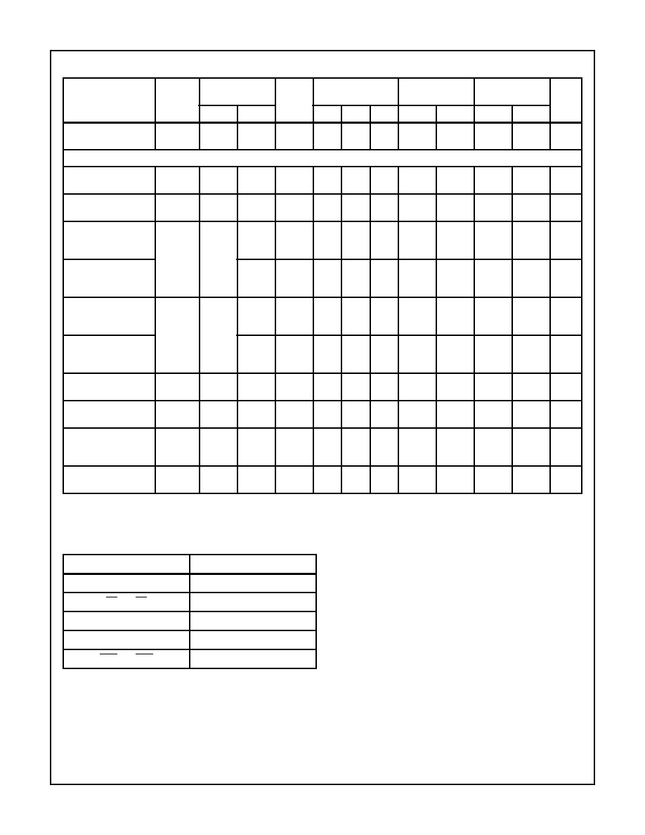
DC Electrical Specifications
(Continued)
PARAMETER
SYMBOL
TEST
CONDITIONS
V
CC
(V)
25
o
C
-40
o
C TO 85
o
C
-55
o
C TO 125
o
C
UNITS
V
I
(V)
I
O
(mA)
MIN
TYP
MAX
MIN
MAX
MIN
MAX
HCT Input Loading Table
INPUT
UNIT LOADS
D0-D3
0.15
E1 and E2
0.15
CP
0.25
MR
0.2
OE1 and OE2
0.5
NOTE: Unit Load is
I
CC
limit specified in DC Electrical
Specifications table, e.g., 360
µ
A max at 25
o
C.
CD54HC173, CD74HC173, CD54HCT173, CD74HCT173