
SN54ALS157A, SN54ALS158
SN74ALS157A, SN74ALS158, SN74AS157, SN74AS158
QUADRUPLE 1-OF-2 DATA SELECTORS/MULTIPLEXERS
SDAS081C ≠ APRIL 1982 ≠ REVISED DECEMBER 1994
Copyright
©
1994, Texas Instruments Incorporated
1
POST OFFICE BOX 655303
∑
DALLAS, TEXAS 75265
∑
Buffered Inputs and Outputs
∑
Package Options Include Plastic
Small-Outline (D) Packages, Ceramic Chip
Carriers (FK), and Standard Plastic (N) and
Ceramic (J) 300-mil DIPs
description
These data selectors/multiplexers contain
inverters and drivers to supply full data selection
to the four output gates. A separate strobe (G)
input is provided. A 4-bit word is selected from one
of two sources and is routed to the four outputs.
The
ALS157A and SN74AS157 present true
data. The
ALS158 and SN74AS158 present
inverted data to minimize propagation delay time.
The SN54ALS157A and SN54ALS158 are
characterized for operation over the full military
temperature range of ≠ 55
∞
C to 125
∞
C. The
SN74ALS157A, SN74ALS158, SN74AS157, and
SN74AS158 are characterized for operation from
0
∞
C to 70
∞
C.
FUNCTION TABLE
INPUTS
OUTPUT Y
G
A /B
DATA
ALS157A
ALS158
G
A /B
A
B
SN74AS157
SN74AS158
H
X
X
X
L
H
L
L
L
X
L
H
L
L
H
X
H
L
L
H
X
L
L
H
L
H
X
H
H
L
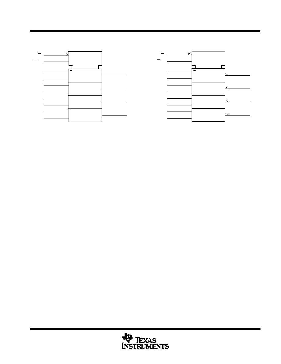
SN54ALS157A, SN54ALS158 . . . J PACKAGE
SN74ALS157A, SN74ALS158,
SN74AS157, SN74AS158 . . . D OR N PACKAGE
(TOP VIEW)
3
2 1 20 19
9 10 11 12 13
4
5
6
7
8
18
17
16
15
14
4A
4B
NC
4Y
3A
1B
1Y
NC
2A
2B
SN54ALS157A, SN54ALS158 . . . FK PACKAGE
(TOP VIEW)
1A
A/B
NC
3Y
3B
G
2Y
GND
NC
V
CC
1
2
3
4
5
6
7
8
16
15
14
13
12
11
10
9
A /B
1A
1B
1Y
2A
2B
2Y
GND
V
CC
G
4A
4B
4Y
3A
3B
3Y
NC ≠ No internal connection
PRODUCTION DATA information is current as of publication date.
Products conform to specifications per the terms of Texas Instruments
standard warranty. Production processing does not necessarily include
testing of all parameters.
SN54ALS157A, SN54ALS158
SN74ALS157A, SN74ALS158, SN74AS157, SN74AS158
QUAD 1-OF-2 DATA SELECTORS/MULTIPLEXERS
SDAS081C ≠ APRIL 1982 ≠ REVISED DECEMBER 1994
2
POST OFFICE BOX 655303
∑
DALLAS, TEXAS 75265
logic symbols
G
MUX
2
1A
1
3
1B
EN
15
G1
1
1Y
4
5
2A
6
2B
2Y
7
11
3A
10
3B
3Y
9
14
4A
13
4B
4Y
12
A /B
1
G
MUX
2
1A
1
3
1B
EN
15
G1
1
1Y
4
5
2A
6
2B
2Y
7
11
3A
10
3B
3Y
9
14
4A
13
4B
4Y
12
A /B
1
ALS157A, SN74AS157
ALS158, SN74AS158
These symbols are in accordance with ANSI/IEEE Std 91-1984 and IEC Publication 617-12.
Pin numbers shown are for the D, J, and N packages.
SN54ALS157A, SN54ALS158
SN74ALS157A, SN74ALS158, SN74AS157, SN74AS158
QUAD 1-OF-2 DATA SELECTORS/MULTIPLEXERS
SDAS081C ≠ APRIL 1982 ≠ REVISED DECEMBER 1994
3
POST OFFICE BOX 655303
∑
DALLAS, TEXAS 75265
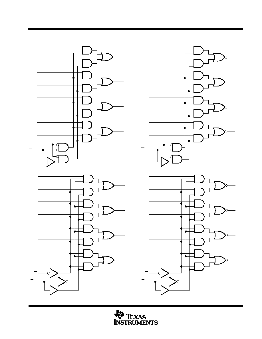
logic diagrams (positive logic)
4Y
3Y
2Y
1Y
12
9
7
4
A /B
G
4B
4A
3B
3A
2B
2A
1B
1A
1
15
13
14
10
11
6
5
3
2
4Y
3Y
2Y
1Y
12
9
7
4
A /B
G
4B
4A
3B
3A
2B
2A
1B
1A
1
15
13
14
10
11
6
5
3
2
ALS157A
ALS158
4Y
3Y
2Y
1Y
12
9
7
4
A /B
G
4B
4A
3B
3A
2B
2A
1B
1A
1
15
13
14
10
11
6
5
3
2
SN74AS157
SN74AS158
4Y
3Y
2Y
1Y
12
9
7
4
A /B
G
4B
4A
3B
3A
2B
2A
1B
1A
1
15
13
14
10
11
6
5
3
2
Pin numbers shown are for the D, J, and N packages.

SN54ALS157A, SN54ALS158
SN74ALS157A, SN74ALS158, SN74AS157, SN74AS158
QUAD 1-OF-2 DATA SELECTORS/MULTIPLEXERS
SDAS081C ≠ APRIL 1982 ≠ REVISED DECEMBER 1994
4
POST OFFICE BOX 655303
∑
DALLAS, TEXAS 75265
absolute maximum ratings over operating free-air temperature range (unless otherwise noted)
Supply voltage, V
CC
7 V
. . . . . . . . . . . . . . . . . . . . . . . . . . . . . . . . . . . . . . . . . . . . . . . . . . . . . . . . . . . . . . . . . . . . . . . .
Input voltage, V
I
7 V
. . . . . . . . . . . . . . . . . . . . . . . . . . . . . . . . . . . . . . . . . . . . . . . . . . . . . . . . . . . . . . . . . . . . . . . . . . . .
Operating free-air temperature range, T
A
: SN54ALS157A, SN54ALS158
≠ 55
∞
C to 125
∞
C
. . . . . . . . . . . . . .
SN74ALS157A, SN74ALS158
0
∞
C to 70
∞
C
. . . . . . . . . . . . . . . . . .
Storage temperature range
≠ 65
∞
C to 150
∞
C
. . . . . . . . . . . . . . . . . . . . . . . . . . . . . . . . . . . . . . . . . . . . . . . . . . . . . . .
Stresses beyond those listed under "absolute maximum ratings" may cause permanent damage to the device. These are stress ratings only, and
functional operation of the device at these or any other conditions beyond those indicated under "recommended operating conditions" is not
implied. Exposure to absolute-maximum-rated conditions for extended periods may affect device reliability.
recommended operating conditions
SN54ALS157A
SN54ALS158
SN74ALS157A
SN74ALS158
UNIT
MIN
NOM
MAX
MIN
NOM
MAX
VCC
Supply voltage
4.5
5
5.5
4.5
5
5.5
V
VIH
High-level input voltage
2
2
V
VIL
Low-level input voltage
0.7
0.8
V
IOH
High-level output current
≠ 0.4
≠ 0.4
mA
IOL
Low-level output current
4
8
mA
TA
Operating free-air temperature
≠ 55
125
0
70
∞
C
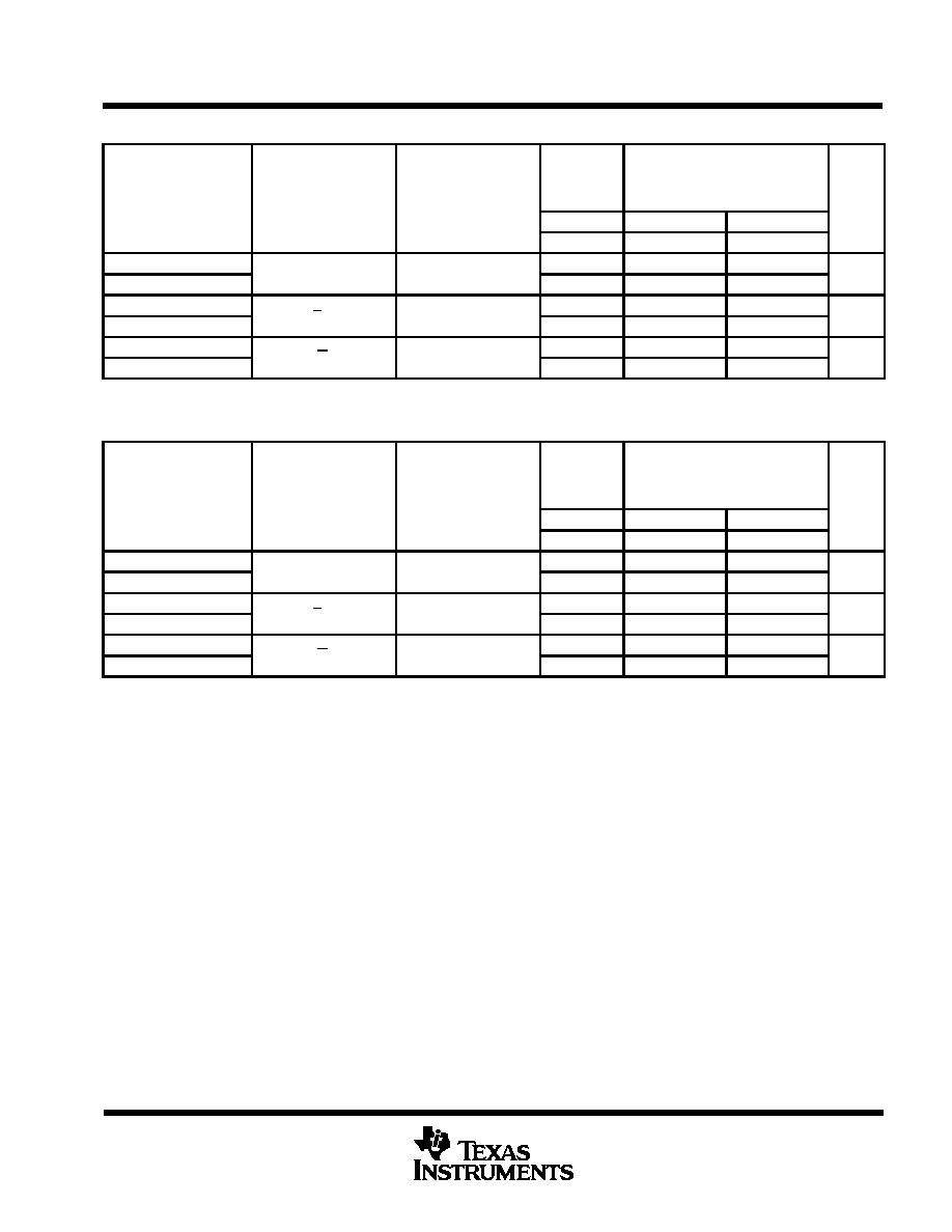
electrical characteristics over recommended operating free-air temperature range (unless
otherwise noted)
PARAMETER
TEST CONDITIONS
SN54ALS157A
SN54ALS158
SN74ALS157A
SN74ALS158
UNIT
MIN
TYP
MAX
MIN
TYP
MAX
VIK
VCC = 4.5 V,
II = ≠ 18 mA
≠ 1.2
≠ 1.2
V
VOH
VCC = 4.5 V to 5.5 V,
IOH = ≠ 0.4 mA
VCC ≠ 2
VCC ≠ 2
V
VOL
VCC = 4 5 V
IOL = 4 mA
0.25
0.4
0.25
0.4
V
VOL
VCC = 4.5 V
IOL = 8 mA
0.35
0.5
V
II
VCC = 5.5 V,
VI = 7 V
0.1
0.1
mA
IIH
VCC = 5.5 V,
VI = 2.7 V
20
20
µ
A
IIL
VCC = 5.5 V,
VI = 0.4 V
≠ 0.1
≠ 0.1
mA
IOß
VCC = 5.5 V,
VO = 2.25 V
≠ 20
≠ 112
≠ 30
≠ 112
mA
ICC
ALS157A
VCC = 5 5 V
See Note 1
6
11
6
11
mA
ICC
ALS158
VCC = 5.5 V,
See Note 1
5
10
5
10
mA
All typical values are at VCC = 5 V, TA = 25
∞
C.
ß The output conditions have been chosen to produce a current that closely approximates one half of the true short-circuit output current, IOS.
NOTE 1: ICC is measured with 4.5 V applied to all inputs and all outputs open.
SN54ALS157A, SN54ALS158
SN74ALS157A, SN74ALS158, SN74AS157, SN74AS158
QUAD 1-OF-2 DATA SELECTORS/MULTIPLEXERS
SDAS081C ≠ APRIL 1982 ≠ REVISED DECEMBER 1994
5
POST OFFICE BOX 655303
∑
DALLAS, TEXAS 75265
switching characteristics (see Figure 1)
PARAMETER
FROM
(INPUT)
TO
(OUTPUT)
VCC = 5 V,
CL = 50 pF,
RL = 500
,
TA = 25
∞
C
VCC = 4.5 V to 5.5 V,
CL = 50 pF,
RL = 500
,
TA = MIN to MAX
UNIT
(INPUT)
(OUTPUT)
ALS157A
SN54ALS157A
SN74ALS157A
TYP
MIN
MAX
MIN
MAX
tPLH
A or B
Y
9
4
17
4
14
ns
tPHL
A or B
Y
6
2
15
2
12
ns
tPLH
A/B
Y
15
7
28
7
24
ns
tPHL
A/B
Y
9
4
20
4
17
ns
tPLH
G
Y
14
7
25
7
20
ns
tPHL
G
Y
10
4
18
4
13
ns
For conditions shown as MIN or MAX, use the appropriate value specified under recommended operating conditions.
switching characteristics (see Figure 1)
PARAMETER
FROM
(INPUT)
TO
(OUTPUT)
VCC = 5 V,
CL = 50 pF,
RL = 500
,
TA = 25
∞
C
VCC = 4.5 V to 5.5 V,
CL = 50 pF,
RL = 500
,
TA = MIN to MAX
UNIT
(INPUT)
(OUTPUT)
ALS158
SN54ALS158
SN74ALS158
TYP
MIN
MAX
MIN
MAX
tPLH
A or B
Y
9
4
18
4
15
ns
tPHL
A or B
Y
5
2
12
2
8
ns
tPLH
A/B
Y
13
5
22
5
18
ns
tPHL
A/B
Y
13
5
22
5
18
ns
tPLH
G
Y
13
5
22
5
18
ns
tPHL
G
Y
13
5
22
5
18
ns
For conditions shown as MIN or MAX, use the appropriate value specified under recommended operating conditions.