MC1489, MC1489A, SN55189, SN55189A, SN75189, SN75189A
QUADRUPLE LINE RECEIVERS
SLLS095D ≠ SEPTEMBER 1973 ≠ REVISED OCTOBER 1998
1
POST OFFICE BOX 655303
∑
DALLAS, TEXAS 75265
D
Input Resistance . . . 3 k
to 7 k
D
Input Signal Range . . .
±
30 V
D
Operate From Single 5-V Supply
D
Built-In Input Hysteresis (Double
Thresholds)
D
Response Control that Provides:
Input Threshold Shifting
Input Noise Filtering
D
Meet or Exceed the Requirements of
TIA / EIA-232-F and ITU Recommendation
V.28
D
Fully Interchangeable With Motorola
TM
MC1489 and MC1489A
description
These devices are monolithic low-power Schottky
quadruple line receivers designed to satisfy the
requirements of the standard interface between
data-terminal equipment and data-communica-
tion equipment as defined by TIA / EIA-232-F. A
separate response-control (CONT) terminal is
provided for each receiver. A resistor or a resistor
and bias-voltage source can be connected
between this terminal and ground to shift the input
threshold levels. An external capacitor can be
connected between this terminal and ground to
provide input noise filtering.
The SN55189 and SN55189A are characterized
for operation over the full military temperature
range of ≠ 55
∞
C to 125
∞
C. The MC1489,
MC1489A, SN75189, and SN75189A are
characterized for operation from 0
∞
C to 70
∞
C.
Copyright
©
1998, Texas Instruments Incorporated
PRODUCTION DATA information is current as of publication date.
Products conform to specifications per the terms of Texas Instruments
standard warranty. Production processing does not necessarily include
testing of all parameters.
Motorola is a trademark of Motorola, Incorporated.
Please be aware that an important notice concerning availability, standard warranty, and use in critical applications of
Texas Instruments semiconductor products and disclaimers thereto appears at the end of this data sheet.
1
2
3
4
5
6
7
14
13
12
11
10
9
8
1A
1CONT
1Y
2A
2CONT
2Y
GND
V
CC
4A
4CONT
4Y
3A
3CONT
3Y
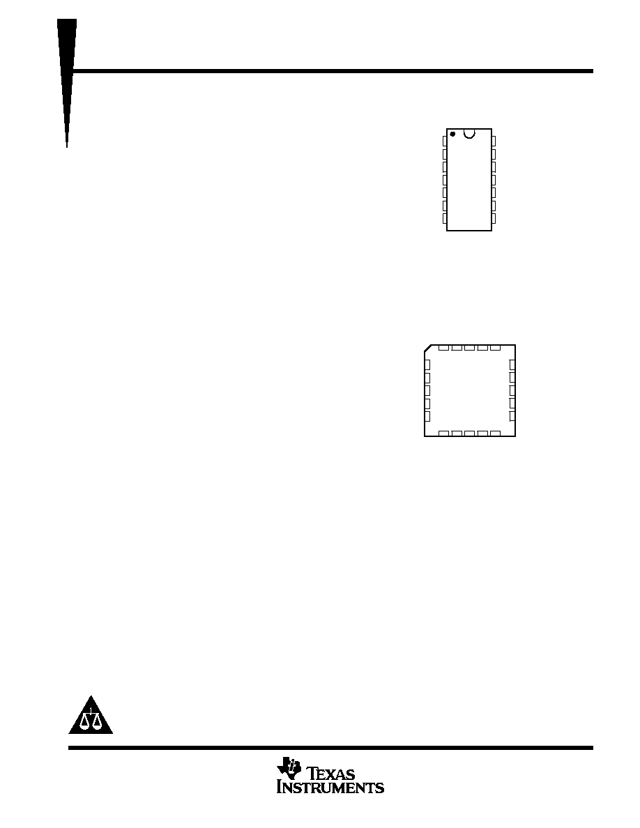
SN55189, SN55189A . . . J OR W PACKAGE
MC1489, MC1489A, SN75189, SN75189A
D, N, OR NS PACKAGE
(TOP VIEW)
3
2
1 20 19
9 10 11 12 13
4
5
6
7
8
18
17
16
15
14
4CONT
NC
4Y
NC
3A
1Y
NC
2A
NC
2CONT
SN55189, SN55189A . . . FK PACKAGE
(TOP VIEW)
1CONT
1A
NC
3Y
3CONT
4A
2Y
GND
NC
NC ≠ No internal connection
CC
V
The NS package is only available left-end taped and reeled.
For SN75189, order SN75189NSR.
On products compliant to MIL-PRF-38535, all parameters are tested
unless otherwise noted. On all other products, production
processing does not necessarily include testing of all parameters.
MC1489, MC1489A, SN55189, SN55189A, SN75189, SN75189A
QUADRUPLE LINE RECEIVERS
SLLS095D ≠ SEPTEMBER 1973 ≠ REVISED OCTOBER 1998
2
POST OFFICE BOX 655303
∑
DALLAS, TEXAS 75265
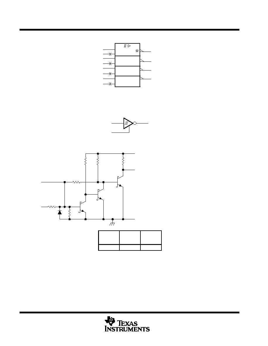
logic symbol
THRS ADJ
4Y
11
3Y
8
2Y
6
1Y
3
1
1A
2
1 CONT
4
2A
5
2 CONT
10
3A
9
3 CONT
13
4A
4 CONT
12
This symbol is in accordance with ANSI/IEEE Std 91-1984 and IEC Publication 617-12.
Pin numbers shown are for the D, J, N, NS, and W packages.
logic diagram (positive logic)
Control
Response
A
Y
schematic (each receiver)
Input A
10 k
4 k
Response
Control
R1
9 k
5 k
1.66 k
GND
Output Y
VCC
MC1489
SN55189
SN75189
MC1489A
SN55189A
SN75189A
R1
8.4 k
1.84 k
Resistor values shown are nominal.
MC1489, MC1489A, SN55189, SN55189A, SN75189, SN75189A
QUADRUPLE LINE RECEIVERS
SLLS095D ≠ SEPTEMBER 1973 ≠ REVISED OCTOBER 1998
3
POST OFFICE BOX 655303
∑
DALLAS, TEXAS 75265
absolute maximum ratings over operating free-air temperature (unless otherwise noted)
Supply voltage, V
CC
(see Note 1)
10 V
. . . . . . . . . . . . . . . . . . . . . . . . . . . . . . . . . . . . . . . . . . . . . . . . . . . . . . . . . . . .
Input voltage, V
I
±
30 V
. . . . . . . . . . . . . . . . . . . . . . . . . . . . . . . . . . . . . . . . . . . . . . . . . . . . . . . . . . . . . . . . . . . . . . . . . .
Output voltage, I
O
20 mA
. . . . . . . . . . . . . . . . . . . . . . . . . . . . . . . . . . . . . . . . . . . . . . . . . . . . . . . . . . . . . . . . . . . . . . . .
Continuous total power dissipation
See Dissipation Rating Table
. . . . . . . . . . . . . . . . . . . . . . . . . . . . . . . . . . . . .
Operating free-air temperature range, T
A
: SN55189, SN55189A
≠ 55
∞
C to 125
∞
C
. . . . . . . . . . . . . . . . . . . . . .
MC1489, MC1489A, SN75189, SN75189A
0
∞
C to 70
∞
C
. . . . . .
Storage temperature range, T
stg
≠ 65
∞
C to 150
∞
C
. . . . . . . . . . . . . . . . . . . . . . . . . . . . . . . . . . . . . . . . . . . . . . . . . . .
Case temperature for 60 seconds, FK package
260
∞
C
. . . . . . . . . . . . . . . . . . . . . . . . . . . . . . . . . . . . . . . . . . . . . .
Lead temperature 1,6 mm (1/16 inch) from case for 60 seconds: J or W package
300
∞
C
. . . . . . . . . . . . . . . .
Lead temperature 1,6 mm (1/16 inch) from case for 10 seconds: D, N, or NS package
260
∞
C
. . . . . . . . . . . .
Stresses beyond those listed under "absolute maximum ratings" may cause permanent damage to the device. These are stress ratings only, and
functional operation of the device at these or any other conditions beyond those indicated under "recommended operating conditions" is not
implied. Exposure to absolute-maximum-rated conditions for extended periods may affect device reliability.
NOTES:
1. All voltage values are with respect to the network ground terminal.
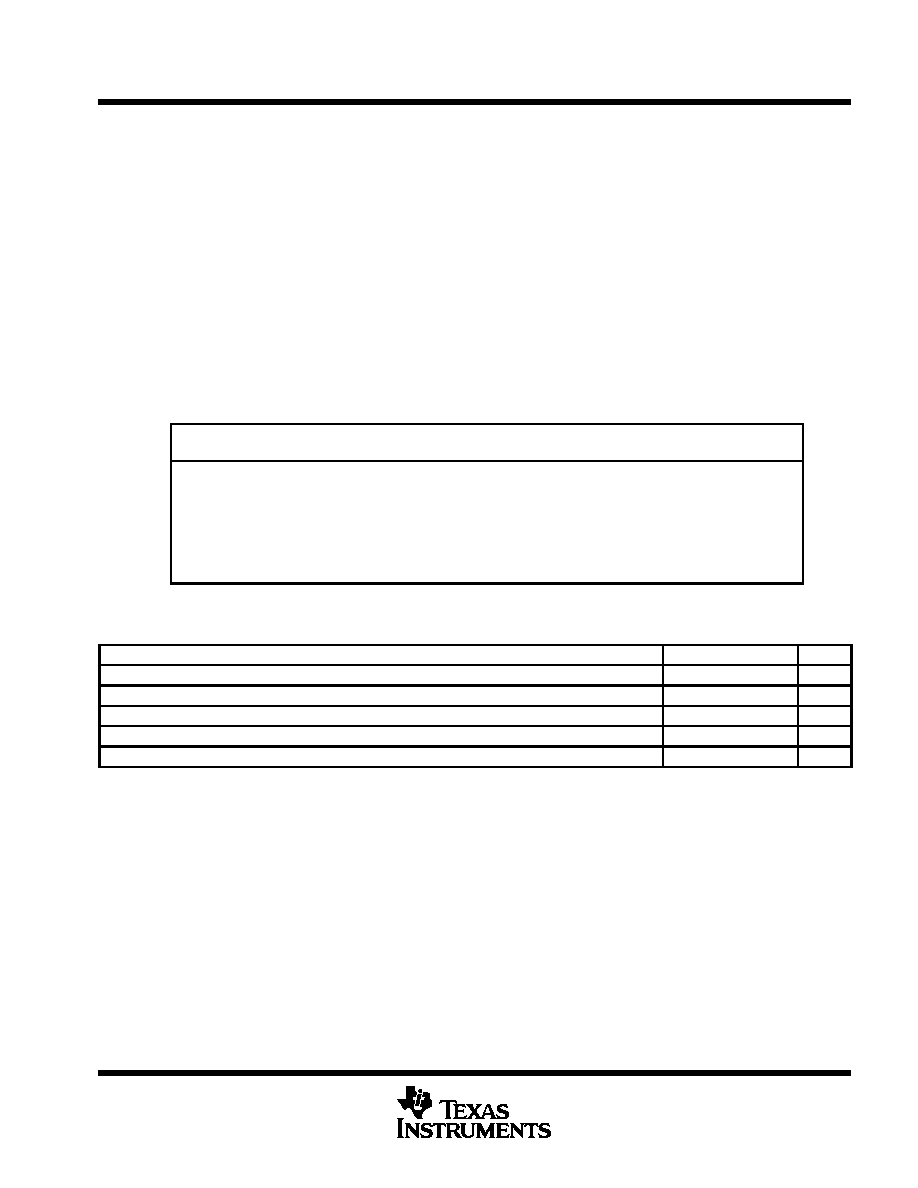
DISSIPATION RATING TABLE
PACKAGE
TA
25
∞
C
DERATING FACTOR
TA = 70
∞
C
TA = 125
∞
C
PACKAGE
A
POWER RATING
ABOVE TA = 25
∞
C
A
POWER RATING
A
POWER RATING
D
950 mW
7.6 mW/
∞
C
608 mW
N/A
FK
1375 mW
11.0 mW/
∞
C
880 mW
275 mW
J
1375 mW
11.0 mW/
∞
C
880 mW
275 mW
N
1150 mW
9.2 mW/
∞
C
736 mW
N/A
NS
625 mW
4.0 mW/
∞
C
445 mW
N/A
W
1000 mW
8.0 mW/
∞
C
640 mW
200 mW
In the J package, SN55189 and SN55189A chips are either silver glass or alloy mounted.
recommended operating conditions
MIN
NOM
MAX
UNIT
Supply voltage, VCC
4.5
5
5.5
V
Input voltage, VI
≠25
25
V
High-level output current, IOH
≠0.5
mA
Low-level output current, IOL
10
mA
Operating free-air temperature, TA
0
70
∞
C
MC1489, MC1489A, SN55189, SN55189A, SN75189, SN75189A
QUADRUPLE LINE RECEIVERS
SLLS095D ≠ SEPTEMBER 1973 ≠ REVISED OCTOBER 1998
4
POST OFFICE BOX 655303
∑
DALLAS, TEXAS 75265
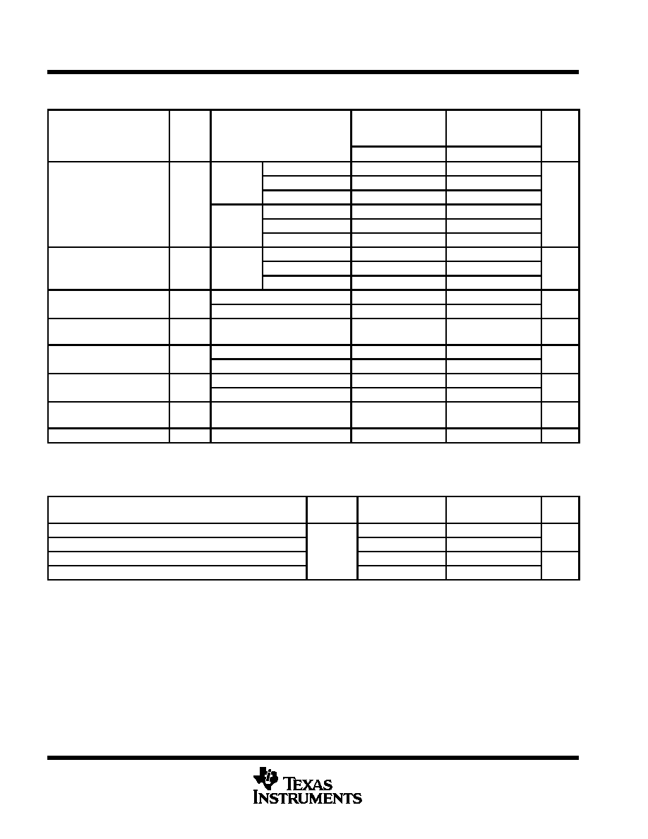
electrical characteristics over operating free-air temperature range, V
CC
= 5 V
±
1% (unless
otherwise noted)
TEST
SN55189
MC1489, MC1489A
SN75189
PARAMETER
TEST
FIGURE
TEST CONDITIONS
SN55189A
SN75189
SN75189A
UNIT
MIN
TYP
MAX
MIN
TYP
MAX
TA = 25
∞
C
1
1.3
1.5
1
1.3
1.5
'89
TA = 0
∞
C to 70
∞
C
0.9
1.6
VIT
Positive-going input
1
TA = ≠ 55
∞
C to 125
∞
C
0.6
1.9
V
VIT+
g
g
threshold voltage
1
TA = 25
∞
C
1.75
1.9
2.25
1.75
1.9
2.25
V
'89A
TA = 0
∞
C to 70
∞
C
1.55
2.25
TA = ≠ 55
∞
C to 125
∞
C
1.30
2.65
N
ti
i
i
t
TA = 25
∞
C
0.75
1.0
1.25
0.75
1.0
1.25
VIT≠
Negative-going input
threshold voltage
1
'89, '89A
TA = 0
∞
C to 70
∞
C
0.65
1.25
V
threshold voltage
TA = ≠ 55
∞
C to 125
∞
C
0.35
1.6
VOH
High-level
1
VI = 0.75 V, IOH = ≠ 0.5 mA
2.6
4
5
2.6
4
5
V
VOH
g
output voltage
1
Input open,
IOH = ≠ 0.5 mA
2.6
4
5
2.6
4
5
V
VOL
Low-level
1
VI = 3 V
IOL = 10 mA
0 2
0 45
0 2
0 45
V
VOL
output voltage
1
VI = 3 V,
IOL = 10 mA
0.2
0.45
0.2
0.45
V
IIH
High-level
2
VI = 25 V
3.6
8.3
3.6
8.3
mA
IIH
g
input current
2
VI = 3 V
0.43
0.43
mA
IIL
Low-level
2
VI = ≠ 25 V
≠ 3.6
≠ 8.3
≠ 3.6
≠8.3
mA
IIL
input current
2
VI = ≠ 3 V
≠ 0.43
≠ 0.43
mA
IOS
Short-circuit
3
3
3
mA
IOS
output current
3
≠ 3
≠3
mA
ICC
Supply current
2
VI = 5 V,
Outputs open
20
26
20
26
mA
All characteristics are measured with the response-control terminal open.
All typical values are at VCC = 5 V, TA = 25
∞
C.
switching characteristics, V
CC
= 5 V, C
L
= 15 pF, T
A
= 25
∞
C
PARAMETER
TEST
TEST CONDITIONS
MIN
TYP
MAX
UNIT
PARAMETER
FIGURE
TEST CONDITIONS
MIN
TYP
MAX
UNIT
tPLH
Propagation delay time, low- to high-level output
RL = 3.9 k
25
85
ns
tPHL
Propagation delay time, high- to low-level output
4
RL = 390
25
50
ns
tTLH
Transition time, low- to high-level output
4
RL = 3.9 k
120
175
ns
tTHL
Transition time, high- to low-level output
RL = 390
10
20
ns
MC1489, MC1489A, SN55189, SN55189A, SN75189, SN75189A
QUADRUPLE LINE RECEIVERS
SLLS095D ≠ SEPTEMBER 1973 ≠ REVISED OCTOBER 1998
5
POST OFFICE BOX 655303
∑
DALLAS, TEXAS 75265
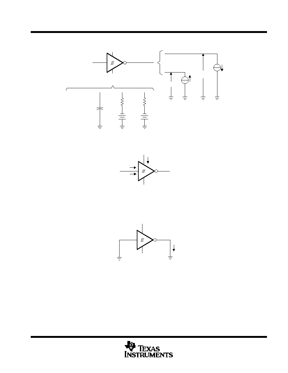
PARAMETER MEASUREMENT INFORMATION
Open
Unless
Otherwise
Specified
CC
≠ VC
RC
+VC
RC
VIT, V1
VCC
VOL
IOL
VOH
≠ IOH
Control
Response
Figure 1. V
IT +
, V
IT ≠
, V
OH
, V
OL
IIL
VI
IIH
VCC
ICC (see Note A)
Open
Response Control Open
NOTE A: ICC is tested for all four receivers simultaneously.
Figure 2. I
IH
, I
IL
, I
CC
≠ IOS
Control
Open
Response
VCC
Figure 3. I
OS
Arrows indicate actual direction of current flow. Current into a terminal is a positive value.