
SPRS009C ≠ JANUARY 1987 ≠ REVISED JULY 1991
TMS320C1x
DIGITAL SIGNAL PROCESSORS
POST OFFICE BOX 1443
∑
HOUSTON, TEXAS 77001
Copyright
©
1991, Texas Instruments Incorporated
1
PRODUCTION DATA information is current as of
publication date. Products conform to specifications
per the terms of Texas Instruments standard warranty.
Production processing does not necessarily include
testing of all parameters.
∑
Performance Up to 8.77 MIPs
∑
All TMS320C1x Devices are Object Code
Compatible
∑
144/256-Word On-Chip Data RAM
∑
1.5K/4K/8K-Word On-Chip Program ROM
∑
4K-Word On-Chip Program EPROM
(TMS320E14/P14/E15/P15/E17/P17)
∑
One-Time Programmable (OTP)
Versions Available (TMS320P14/P15/P17)
∑
EPROM Code Protection for Copyright
Security
∑
4K / 64K-Word Total External Memory at
Full Speed
∑
32-Bit ALU/Accumulator
∑
16
◊
16-Bit Multiplier With a 32-Bit Product
∑
0 to 16-Bit Barrel Shifter
∑
Eight Input/Output Channels
∑
Dual-Channel Serial Port
∑
Simple Memory and I/O Interface
∑
5-V and 3.3-V Versions Available
(TMS320LC15/LC17)
∑
Commercial and Military Versions Available
∑
Operating Free-Air Temperature
. . . 0
∞
C to 70
∞
C
∑
Packaging: DIP, PLCC, Quad Flatpack, and
CER-QUAD
∑
CMOS Technology:
Device
Cycle Time
-- TMS320C10
200-ns
. . . . . . . . . . . . . . . . . . .
-- TMS320C10-14
280-ns
. . . . . . . . . . . . . . . .
-- TMS320C10-25
160-ns
. . . . . . . . . . . . . . . .
-- TMS320C14
160-ns
. . . . . . . . . . . . . . . . . . .
-- TMS320E14
160-ns
. . . . . . . . . . . . . . . . . . .
-- TMS320P14
160-ns
. . . . . . . . . . . . . . . . . . .
-- TMS320C15
200-ns
. . . . . . . . . . . . . . . . . . .
-- TMS320C15-25
160-ns
. . . . . . . . . . . . . . . .
-- TMS320E15
200-ns
. . . . . . . . . . . . . . . . . . .
-- TMS320E15-25
160-ns
. . . . . . . . . . . . . . . .
-- TMS320LC15
250-ns
. . . . . . . . . . . . . . . . . .
-- TMS320P15
200-ns
. . . . . . . . . . . . . . . . . . .
-- TMS320C16
114-ns
. . . . . . . . . . . . . . . . . . .
-- TMS320C17
200-ns
. . . . . . . . . . . . . . . . . . .
-- TMS320E17
200-ns
. . . . . . . . . . . . . . . . . . .
-- TMS320LC17
278-ns
. . . . . . . . . . . . . . . . . .
-- TMS320P17
200-ns
. . . . . . . . . . . . . . . . . . .
introduction
The TMS32010 digital signal processor (DSP), introduced in 1983, was the first DSP in the TMS320 family. From
it has evolved this TMS320C1x generation of 16-bit DSPs. All
C1x DSPs are object code compatible with the
TMS32010 DSP. The
C1x DSPs combine the flexibility of a high-speed controller with the numerical capability
of an array processor, thereby offering an inexpensive alternative to multichip bit-slice processors. The highly
paralleled architecture and efficient instruction set provide speed and flexibility to produce a CMOS
microprocessor generation capable of executing up to 8.77 MIPS (million instructions per second) (
C16). These
C1x devices utilize a modified Harvard architecture to optimize speed and flexibility, implementing functions in
hardware that other processors implement through microcode or software.
The
C1x generation's powerful instruction set, inherent flexibility, high-speed number-handling capabilities,
reduced power consumption, and innovative architecture have made these cost-effective DSPs the ideal
solution for many telecommunications, computer, commercial, industrial, and military applications.
This data sheet provides detailed design documentation for the
C1x DSPs. It facilitates the selection of devices
best suited for various user applications by providing specifications and special features for each
C1x DSP.
This data sheet is arranged as follows: introduction, quick reference table of device parameters and packages,
summary overview of each device, architecture overview, and the
C1x device instruction set summary. These
are followed by data sheets for each
C1x device providing available package styles, terminal function tables,
block diagrams, and electrical and timing parameters. An index is provided to facilitate data sheet usage.

DEVICE
SPRS009C ≠ JANUARY 1987 ≠ REVISED JULY 1991
TMS320C1x
DIGITAL SIGNAL PROCESSORS
POST OFFICE BOX 1443
∑
HOUSTON, TEXAS 77001
2
Table 1 provides an overview of
C1x processors with comparisons of memory, I/O, cycle timing, military support,
and package types. For specific availability, contact the nearest TI Field Sales Office.
Table 1. TMS320C1x Device Overview
MEMORY
I/O
CYCLE
PACKAGE (1)
RAM
ROM
EPROM
PROG.
SERIAL
PARALLEL
(ns)
DIP
PLCC
CER-QUAD
TMS320C10 (2)
144
1.5K
--
4K
--
8
◊
16
200
40
44
--
TMS320C10-14
144
1.5K
--
4K
--
8
◊
16
280
40
44
--
TMS320C10-25
144
1.5K
--
4K
--
8
◊
16
160
40
44
--
TMS320C14 (3)
256
4K
--
4K
1
7
◊
16 (4)
160
--
68
--
TMS320E14 (3)
256
--
4K
4K
1
7
◊
16 (4)
160
--
--
68 CER
TMS320P14
256
--
4K
4K
1
7
◊
16 (4)
160
--
68
--
TMS320C15 (3)
256
4K
--
4K
--
8
◊
16
200
40
44
--
TMS320C15-25
256
4K
--
4K
--
8
◊
16
160
40
44
--
TMS320E15 (3)
256
--
4K
4K
--
8
◊
16
200
40
--
44 CER
TMS320E15-25
256
--
4K
4K
--
8
◊
16
160
40
--
44 CER
TMS320LC15
256
4K
--
4K
--
8
◊
16
250
40
44
--
TMS320P15
256
--
4K
4K
--
8
◊
16
200
40
44
--
TMS320C16
256
8K
--
64K
--
8
◊
16
114
--
--
64 QFP
TMS320C17
256
4K
--
--
2
6
◊
16 (5)
200
40
44
--
TMS320E17 (5)
256
--
4K
--
2
6
◊
16 (5)
200
40
--
44 CER
TMS320LC17 (5)
256
4K
--
--
2
6
◊
16 (5)
278
40
44
--
TMS320P17 (5)
256
--
4K
--
2
6
◊
16 (5)
200
40
44
One-time programmable (OTP) device is in a windowless plastic package and cannot be erased.
NOTES: 1. DIP = dual in-line package. PLCC = plastic-leaded chip carrier. CER = ceramic-leaded chip carrier. QFP = plastic quad flat pack.
2. Military version available.
3. Military versions planned; contact nearest TI Field Sales Office for availability.
4. On-chip 16-bit I/O, four capture inputs, and six compare outputs are available.
5. On-chip 16-bit coprocessor interface is optional by pin selection.

SPRS009C ≠ JANUARY 1987 ≠ REVISED JULY 1991
TMS320C1x
DIGITAL SIGNAL PROCESSORS
POST OFFICE BOX 1443
∑
HOUSTON, TEXAS 77001
3
description
TMS320C10
The
C10 provides the core CPU used in all other
C1x devices. Its microprocessor operates at 5 MIPS. It
provides a parallel I/O of 8
◊
16 bits. Three versions with cycle times of 160, 200, and 280 ns are available as
illustrated in Table 1. The
C10 versions are offered in plastic 40-pin DIP or a 44-lead PLCC packages.
TMS320C14/E14/P14
The
C14/E14/P14 devices, using the
C10 core CPU, offer expanded on-chip RAM, and ROM or EPROM
(
E14/P14), 16 pins of bit selectable parallel I/O, an I/O mapped asynchronous serial port, four 16-bit timers, and
external/internal interrupts. The
C14 devices can provide for microcomputer/microprocessor operating modes.
Three versions with cycle times of 160-ns are available as illustrated in Table 1. These devices are offered in
68-pin plastic PLCC or ceramic CER-QUAD packages.
TMS320C15/E15/P15
The
C15/E15/P15 devices are a version of the
C10, offering expanded on-chip RAM, and ROM or EPROM
(
E15/P15). The
P15 is a one-time programmable (OTP), windowless EPROM version. These devices can
operate in the microcomputer or microprocessor modes. Five versions are available with cycle times of 160 to
200 ns (see Table 1). These devices are offered in 40-pin DIP, 44-pin PLCC, or 44-pin ceramic packages.
TMS320LC15
The
LC15 is a low-power version of the
C15, utilizing a V
DD
of only 3.3-V. This feature results in a 2.3: 1 power
requirement reduction over the typical 5-V
C1x device. It operates at a cycle time of 250 ns. The device is offered
in 40-pin DIP or 44-lead PLCC packages.
TMS320C16
The
C16 offers on-chip RAM of 256-words, an expanded program memory of 64K-words, and a fast instruction
cycle time of 114 ns (8.77 MIPS). It is offered in a 64-pin quad flat-pack package.
TMS320C17/E17/P17
The
C17/E17/P17 versions consist of five major functional units: the
C15 microcomputer, a system control
register, a full-duplex dual channel serial port,
µ
-law/A-law companding hardware, and a coprocessor port. The
dual-channel serial port is capable of full-duplex serial communication and offers direct interface to two
combo-codecs. The hardware companding logic can operate in either
µ
-law or A-law format with either
sign-magnitude or twos complement numbers in either serial or parallel modes. The coprocessor port allows
the
C17/E17/P17 to act as a slave microcomputer or as a master to a peripheral microcomputer.
The
P17 utilizes a one-time programmable (OTP) windowless EPROM version of the
E17.
TMS320LC17
The
LC17 is a low-power version of the
C17, utilizing a V
DD
of only 3.3-V. This feature results in a
2.3: 1 power requirement reduction over the typical 5-V
C1x device. It operates at a cycle time of 278 ns.
SPRS009C ≠ JANUARY 1987 ≠ REVISED JULY 1991
TMS320C1x
DIGITAL SIGNAL PROCESSORS
POST OFFICE BOX 1443
∑
HOUSTON, TEXAS 77001
4
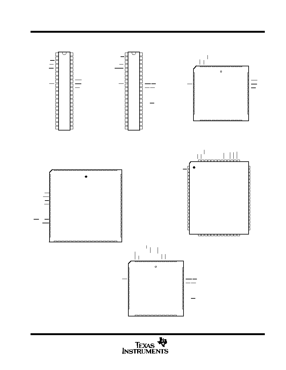
1
2
3
4
5
6
7
8
9
10
11
12
13
14
15
16
17
18
19
20
40
39
38
37
36
35
34
33
32
31
30
29
28
27
26
25
24
23
22
21
A1/PA1
A0/PA0
MC/MP
RS
INT
CLKOUT
X1
X2/CLKIN
BIO
VSS
D8
D9
D10
D11
D12
D13
D14
D15
D7
D6
A2/PA2
A3
A4
A5
A6
A7
A8
MEN
DEN
WE
VCC
A9
A10
A11
D0
D1
D2
D3
D4
D5
TMS320C10/C15/LC15/P15
N/JD Packages
(Top View)
TMS320C10/C15/E15/LC15/P15
FN/FZ Packages
(Top View)
CLKOUT
X1
X2/CLKIN
BIO
NC
VSS
D8
D9
D10
D11
D12
A7
A8
MEN
DEN
WE
VCC
A9
A10
A11
D0
D1
1
2
3
4
5
6
7
8
9
10
11
12
13
14
15
16
17
18 19 20 21 22 23 24 25 26 27 28
44 43 42 41 40
39
38
37
36
35
34
33
32
31
30
29
INT
RS
MC/MP
A0/P
A0
A1/P
A1
A2/P
A2
A3
A4
A5
A6
D13
D14
D15
D7
D6
D5
D4
D3
D2
CC
V
CC
V
V
CC
NC
NC
A0/PA0
A1/PA1
A2/PA2
A3
A4
A5
A6
VSS
A7
A8
A9
A10
A11
A12
1
2
3
4
5
6
7
8
9
10
11
12
13
14
15
16
17
18
19
51
50
49
48
47
46
45
44
43
42
41
40
39
38
37
36
35
34
33
A13
A14
NC
NC
RS
X1
X2/CLKIN
VSS
VSS
VSS
VSS
CLKOUT
D15
D14
NC
D13
D12
D11
D10
D9
NC
NC
20212223242526272829303132
64636261605958575655545352
D8
D7
D6
D5
D4
D3
D2
NC
D1
D0
A15
NC
BIO
INT
MC/MP
V
V
V
MEN
NC
IOEN
MWE
IOWE
V
DD
DD
DD
DD
V
DD
V
SS
TMS320C16
PG Package
(Top View)
1
2
3
4
5
6
7
8
9
10
11
12
13
14
15
16
17
18
19
20
40
39
38
37
36
35
34
33
32
31
30
29
28
27
26
25
24
23
22
21
PA1/RBLE
PA0/HI/LO
MC
RS
EXINT
CLKOUT
X1
X2/CLKIN
BIO
VSS
D8/LD8
D9/LD9
D10/Ld10
D11/LD11
D12/LD12
D13/LD13
D14/LD14
D15/LD15
D7/LD7
D6/LD6
PA2/TBLF
FSR
FSX
FR
DX1
DX0
SCLK
DR1
DEN/RD
WE/WR
VCC
DR0
XF
MC/PM
D0/LD0
D1/LD1
D2/LD2
D3/LD3
D4/LD4
D5/LD5
TMS320C17/E17/LC17/P17
N/JD Packages
(Top View)
D4
D5
D6
D7
IOP0
IOP1
IOP2
IOP3
IOP4
IOP5
D8
A9
CMP0
CMP1
A10
A1
1
CMP2
AMP4/CAP2/FSR
D0
D1
D9
RXD/DATA
TXD/CLK
D10
IOP6
IOP7
10
11
12
13
14
15
16
17
18
19
20
21
22
23
24
25
26
27 28 29 30 31 32 33 34 35 36 37 38 39 40 41 42 43
9 8 7 6 5 4 3 2 1 68 67 66 65 64 63 62 61
TCLK/CLKR
TCLK2/CLKX
A8
A7
A6
WE
REN
RS
INT
CLKOUT
A5
A4
NMI/MC/MP
WDT
CLKIN
A3
A2
60
59
58
57
56
55
54
53
52
51
50
49
48
47
46
45
44
A0
IOP15
IOP14
IOP13
IOP12
D14
IOP1
1
IOP10
D13
D12
IOP9
IOP8
D1
1
A1
D15
D3
D2
TMS320C14/E14/P14
FN/FZ Packages
(Top View)
1
2
3
4
5
6
7
8
9
10
11
12
13
14
15
16
17
18 19 20 21 22 23 24 25 26 27 28
44 43 42 41 40
39
38
37
36
35
34
33
32
31
30
29
EXINT
RS
MC
P
AO/HI/LO
P
A1/RBLE
P
A2/TBLF
FSR
FSX
FR
DX1
D13/LD13
D14/LD14
D15/LD15
D7/LD7
D6/LD6
D5/LD5
D4/LD4
D3/LD3
D2/LD2
SS
V
D1/LD1
V
SS
CLKOUT
X1
X2/CLKIN
BIO
NC
VSS
D8
D9
D10
D11
D12
DX0
SCLK
DR1
DEN/RD
WE/WR
VCC
DR0
XF
MC/PM
D0/LD0
VSS
TMS320C17/E17
FN/FZ Packages
(Top View)
V
CC1
V
SS1
V
CC2
V
SS2
CMP3
CAP0
CAP1
CMP5/CAP3/FSX

SPRS009C ≠ JANUARY 1987 ≠ REVISED JULY 1991
TMS320C1x
DIGITAL SIGNAL PROCESSORS
POST OFFICE BOX 1443
∑
HOUSTON, TEXAS 77001
5
architecture
The
C1x DSPs use a modified Harvard architecture for speed and flexibility. In a strict Harvard architecture,
program and data memory lie in two separate spaces, permitting a full overlap of instruction fetch and one-cycle
execution. The
C1x DSPs modification allows transfers between program and data spaces, thereby increasing
the flexibility of the device. This modification permits coefficients stored in program memory to be read into the
RAM, eliminating the need for a separate coefficient ROM.
32-bit accumulator
All
C1x devices contain a 32-bit ALU and accumulator for support of double-precision, twos-complement
arithmetic. The ALU is a general-purpose arithmetic unit that operates on 16-bit words taken from the data RAM
or derived from immediate instructions. In addition to the usual arithmetic instructions, the ALU can perform
Boolean operations, providing the bit manipulation ability required of a high-speed controller. The accumulator
stores the output from the ALU and is often an input to the ALU. It operates with a 32-bit word length. The
accumulator is divided into a high-order word (bits 31 through 16) and a low-order word (bits 15 through 0).
Instructions are provided for storing the high- and low-order accumulator words in memory.
shifters
Two shifters are available for manipulating data. The ALU barrel shifter performs a left-shift of 0 to 16 places
on data memory words loaded into the ALU. This shifter extends the high-order bit of the data word and zero-fills
the low-order bits for twos-complement arithmetic. The accumulator parallel shifter performs a left-shift of 0, 1
or 4 places on the entire accumulator and places the resulting high-order accumulator bits into data RAM. Both
shifters are useful for scaling and bit extraction.
16
◊
16-bit parallel multiplier
The multiplier performs a 16
◊
16-bit twos-complement multiplication with a 32-bit result in a single instruction
cycle. The multiplier consists of three units: the T Register, P Register, and a multiplier array. The 16-bit T
Register stores the multiplicand, and the P Register stores the 32-bit product. Multiplier values either come from
the data memory or are derived immediately from the MPYK (multiply immediate) instruction word. The fast
on-chip multiplier allows the device to perform fundamental operations such as convolution, correlation, and
filtering.
data and program memory
Since the
C1x devices use a Harvard type architecture, data and program memory reside in two separate
spaces. These DSP devices have 144-or 256-words of on-chip data RAM and 1.5K- to 8K-words of on-chip
program ROM. On-chip program EPROM of 4K-words is provided in the
E14/E15/E17 devices. An on-chip
one-time programmable 4K-word EPROM is provided in the
P14/P15/P17 devices. The EPROM cell utilizes
standard PROM programmers and is programmed identically to a 64K CMOS EPROM (TMS27C64).
(Reference Table 1.)
program memory expansion
All
C1x devices except the
C17/E17/LC17/P17 devices are capable of executing from off-chip external memory
at full speed for those applications requiring external program memory space. This allows for external
RAM-based systems to provide multiple functionality. The
C17/E17/LC17/P17 devices provide no external
memory expansion. (Reference Table 1.)
microcomputer/microprocessor operating modes
All devices except the
x17 offer two modes of operation defined by the state of the MC/MP pin: the
microcomputer mode (MC/MP = 1) or the microprocessor mode (MC/MP = 0 ). In the microcomputer mode,
on-chip ROM is mapped into the program memory space. In the microprocessor mode, all words of progam
memory are external.