TLC372
LinCMOS DUAL DIFFERENTIAL COMPARATORS
SLCS114D - NOVEMBER 1983 - REVISED APRIL 2004
1
POST OFFICE BOX 655303
∑
DALLAS, TEXAS 75265
D
Single or Dual-Supply Operation
D
Wide Range of Supply Voltages 2 V to 18 V
D
Low Supply Current Drain
150
µ
A Typ at 5 V
D
Fast Response Time . . . 200 ns Typ for
TTL-Level Input Step
D
Built-in ESD Protection
D
High Input Impedance . . . 10
12
Typ
D
Extremely Low Input Bias Current
5 pA Typ
D
Ultrastable Low Input Offset Voltage
D
Input Offset Voltage Change at Worst-Case
Input Conditions Typically 0.23
µ
V/Month,
Including the First 30 Days
D
Common-Mode Input Voltage Range
Includes Ground
D
Output Compatible With TTL, MOS, and
CMOS
D
Pin-Compatible With LM393
description
This device is fabricated using LinCMOS
technology and consists of two independent
voltage comparators, each designed to operate
from a single power supply. Operation from dual
supplies is also possible if the difference between
the two supplies is 2 V to 18 V. Each device
features extremely high input impedance
(typically greater than 10
12
), allowing direct
interfacing with high-impedance sources. The
outputs are n-channel open-drain configurations
and can be connected to achieve positive-logic
wired-AND relationships.
The TLC372 has internal electrostatic discharge
(ESD) protection circuits and has been classified
with a 1000-V ESD rating using human body
model testing. However, care should be exercised
in handling this device as exposure to ESD may
result in a degradation of the device parametric
performance.
The TLC372C is characterized for operation from 0
∞
C to 70
∞
C. The TLC372I is characterized for operation from
-40
∞
C to 85
∞
C. The TLC372M is characterized for operation over the full military temperature range of - 55
∞
C
to 125
∞
C. The TLC372Q is characterized for operation from - 40
∞
C to 125
∞
C.
Please be aware that an important notice concerning availability, standard warranty, and use in critical applications of
Texas Instruments semiconductor products and disclaimers thereto appears at the end of this data sheet.
Copyright
1983 - 2004, Texas Instruments Incorporated
PRODUCTION DATA information is current as of publication date.
Products conform to specifications per the terms of Texas Instruments
standard warranty. Production processing does not necessarily include
testing of all parameters.
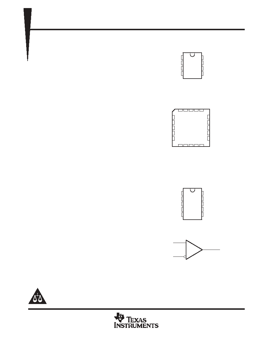
1
2
3
4
8
7
6
5
1OUT
1IN -
1IN +
GND
V
CC
2OUT
2IN -
2IN +
TLC372C, TLC372I, TLC372M, TLC372Q
D, P, OR PW PACKAGE
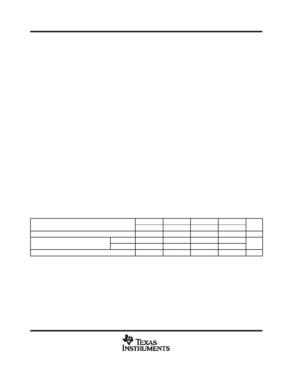
TLC372M . . . JG PACKAGE
(TOP VIEW)
3
2
1 20 19
9 10 11 12 13
4
5
6
7
8
18
17
16
15
14
NC
2OUT
NC
2IN -
NC
NC
1IN -
NC
1IN +
NC
TLC372M . . . FK PACKAGE
(TOP VIEW)
NC
1OUT
NC
2IN+
NC
NC
NC
GND
NC
OUT
IN +
symbol (each comparator)
IN -
NC - No internal connection
V
DD
1
2
3
4
5
10
9
8
7
6
NC
1OUT
1IN-
1IN+
GND
NC
V
CC
2OUT
2IN-
2IN+
TLC372M
U PACKAGE
(TOP VIEW)
LinCMOS is a trademark of Texas Instruments Incorporated. All other trademarks are the property of their respective owners.

TLC372
LinCMOS DUAL DIFFERENTIAL COMPARATORS
SLCS114D - NOVEMBER 1983 - REVISED APRIL 2004
2
POST OFFICE BOX 655303
∑
DALLAS, TEXAS 75265
equivalent schematic (each comparator)
Common to All Channels
VDD
GND
OUT
IN +
IN -
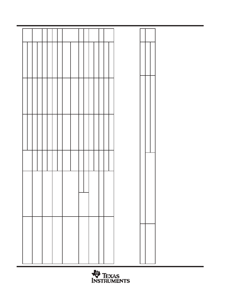
AVAILABLE OPTIONS
V
max
PACKAGED DEVICES
TA
VIO max
AT 25
∞
C
SMALL
OUTLINE
(D)
CHIP
CARRIER
(FK)
CERAMIC
DIP
(JG)
PLASTIC
DIP
(P)
TSSOP
(PW)
CERAMIC
FLAT PACK
(U)
0
∞
C to 70
∞
C
5 mV
TLC372CD
--
--
TLC372CP
TLC372CPW
--
- 40
∞
C to 85
∞
C
5 mV
TLC372ID
--
--
TLC372IP
--
--
- 55
∞
C to 125
∞
C
5 mV
TLC372MD
TLC372MFK
TLC372MJG
TLC372MP
--
TLC372MU
- 40
∞
C to 125
∞
C
5 mV
TLC372QD
--
--
TLC372QP
--
--
The D packages are available taped and reeled. Add R suffix to device type (e.g., TLC372CDR).
TLC372
LinCMOS DUAL DIFFERENTIAL COMPARATORS
SLCS114D - NOVEMBER 1983 - REVISED APRIL 2004
3
POST OFFICE BOX 655303
∑
DALLAS, TEXAS 75265
absolute maximum ratings over operating free-air temperature range (unless otherwise noted)
Supply voltage, V
DD
(see Note 1)
18 V
. . . . . . . . . . . . . . . . . . . . . . . . . . . . . . . . . . . . . . . . . . . . . . . . . . . . . . . . . . . .
Differential input voltage, V
ID
(see Note 2
±
18 V
. . . . . . . . . . . . . . . . . . . . . . . . . . . . . . . . . . . . . . . . . . . . . . . . . . . .
Input voltage range, V
I
-0.3 V to 18 V
. . . . . . . . . . . . . . . . . . . . . . . . . . . . . . . . . . . . . . . . . . . . . . . . . . . . . . . . . . . . .
Output voltage, V
O
18 V
. . . . . . . . . . . . . . . . . . . . . . . . . . . . . . . . . . . . . . . . . . . . . . . . . . . . . . . . . . . . . . . . . . . . . . . . .
Input current, I
I
±
5 mA
. . . . . . . . . . . . . . . . . . . . . . . . . . . . . . . . . . . . . . . . . . . . . . . . . . . . . . . . . . . . . . . . . . . . . . . . . .
Output current, I
O
20 mA
. . . . . . . . . . . . . . . . . . . . . . . . . . . . . . . . . . . . . . . . . . . . . . . . . . . . . . . . . . . . . . . . . . . . . . . .
Duration of output short circuit to ground (see Note 3)
unlimited
. . . . . . . . . . . . . . . . . . . . . . . . . . . . . . . . . . . . . .
Package thermal impedance,
JA
(see Notes 4 and 5): D package
97.1
∞
C/W
. . . . . . . . . . . . . . . . . . . . . . . . . .
P package
84.6
∞
C/W
. . . . . . . . . . . . . . . . . . . . . . . . . .
PW package
149
∞
C/W
. . . . . . . . . . . . . . . . . . . . . . . . .
Package thermal impedance,
JC
(see Notes 4 and 5): FK package
5.6
∞
C/W
. . . . . . . . . . . . . . . . . . . . . . . . . . .
JG package
14.5
∞
C/W
. . . . . . . . . . . . . . . . . . . . . . . . .
U package
14.7
∞
C/W
. . . . . . . . . . . . . . . . . . . . . . . . . .
Operating free-air temperature range, T
A
: TLC372C 0
∞
C to 70
∞
C
. . . . . . . . . . . . . . . . . . . . . . . . . . . . . . . . . . . . .
TLC372I -40
∞
C to 85
∞
C
. . . . . . . . . . . . . . . . . . . . . . . . . . . . . . . . . . . .
TLC372M -55
∞
C to 125
∞
C
. . . . . . . . . . . . . . . . . . . . . . . . . . . . . . . . . .
TLC372Q -40
∞
C to 125
∞
C
. . . . . . . . . . . . . . . . . . . . . . . . . . . . . . . . . .
Storage temperature range
-65
∞
C to 150
∞
C
. . . . . . . . . . . . . . . . . . . . . . . . . . . . . . . . . . . . . . . . . . . . . . . . . . . . . . . .
Case temperature for 60 seconds: FK package
260
∞
C
. . . . . . . . . . . . . . . . . . . . . . . . . . . . . . . . . . . . . . . . . . . . . .
Lead temperature 1,6 mm (1/16 inch) from case for 10 seconds: D, P, or PW package
260
∞
C
. . . . . . . . . . . .
Lead temperature 1,6 mm (1/16 inch) from case for 60 seconds: JG or U package
300
∞
C
. . . . . . . . . . . . . . .
Stresses beyond those listed under "absolute maximum ratings" may cause permanent damage to the device. These are stress ratings only, and
functional operation of the device at these or any other conditions beyond those indicated under "recommended operating conditions" is not
implied. Exposure to absolute-maximum-rated conditions for extended periods may affect device reliability.
NOTES:
1. All voltage values except differential voltages are with respect to network ground.
2. Differential voltages are at IN+ with respect to IN -.
3. Short circuits from outputs to VDD can cause excessive heating and eventual device destruction.
4. Maximum power dissipation is a function of TJ(max),
JA, and TA. The maximum allowable power dissipation at any allowable
ambient temperature is PD = (TJ(max) - TA)/
JA. Operating at the absolute maximum TJ of 150
∞
C can affect reliability.
5. The package thermal impedance is calculated in accordance with JESD 51-7 (plastic) or MIL-STD-883 Method 1012 (ceramic).
recommended operating conditions
TLC372C
TLC372I
TLC372M
TLC372Q
UNIT
MIN
MAX
MIN
MAX
MIN
MAX
MIN
MAX
UNIT
Supply voltage, VDD
3
16
3
16
4
16
4
16
V
Common-mode input voltage, VIC
VDD = 5 V
0
3.5
0
3.5
0
3.5
0
3.5
V
Common-mode input voltage, VIC
VDD = 10 V
0
8.5
0
8.5
0
8.5
0
8.5
V
Operating free-air temperature, TA
0
70
- 40
85
- 55
125
- 40
125
∞
C
TLC372
SLCS114D - NOVEMBER 1983 - REVISED APRIL 2004
Template Release Date: 7-11-94
DUAL DIFFERENTIAL COMPARATORS
LinCMOS
4
POST OFFICE BOX 655303 DALLAS, TEXAS 75265
∑
electrical characteristics at specified free-air temperature, V
DD
= 5 V (unless otherwise noted)
P
ARAMETER
TEST CONDITIONS
T
A
TLC372C
TLC372I
TLC372M, TLC372Q
UNIT
P
ARAMETER
TEST CONDITIONS
T
A
MIN
TYP
MAX
MIN
TYP
MAX
MIN
TYP
MAX
UNIT
V
IO
Input of
fset voltage
V
IC
= V
ICR
min,
See Note 4
25
∞
C
1
5
1
5
1
5
mV
V
IO
Input of
fset voltage
V
IC
= V
ICR
min
,
See Note 4
Full range
6.5
7
10
mV
I IO
Input of
fset current
25
∞
C
1
1
1
pA
I IO
Input of
fset current
MAX
0.3
1
10
nA
I IB
Input bias current
25
∞
C
5
5
5
pA
I IB
Input bias current
MAX
0.6
2
20
nA
V
ICR
Common-mode input
25
∞
C
0 to
V
DD
-1
0 to
V
DD
-1
0 to
V
DD
-1
V
V
ICR
Common-mode input
voltage range
Full range
0 to
V
DD
-1.5
0 to
V
DD
-1.5
0 to
V
DD
-1.5
V
I OH
High-level output current
V
ID
= 1 V
V
OH
= 5 V
25
∞
C
0.1
0.1
0.1
nA
I OH
High-level output current
V
ID
= 1 V
V
OH
= 15 V
Full range
1
1
3
µ
A
V
OL
Low-level output voltage
V
ID
= -
1
V
,
I OL
= 4 mA
25
∞
C
150
400
150
400
150
400
mV
V
OL
Low-level output voltage
V
ID
= -
1
V
,
I OL
= 4 mA
Full range
700
700
700
mV
I OL
Low-level output current
V
ID
= -
1
V
,
V
OL
= 1.5 V
25
∞
C
6
16
6
16
6
16
mA
I DD
Supply current
V
ID
= 1 V
,
No load
25
∞
C
150
300
150
300
150
300
µ
A
I DD
Supply current
(two comparators)
V
ID
= 1 V
,
No load
Full range
400
400
400
µ
A
All characteristics are measured with zero common-mode input voltage unless otherwise noted. Full range is 0
∞
C to 70
∞
C for TLC372C, -
4
0
∞
C to 85
∞
C for TLC372I, and -
5
5
∞
C to
125
∞
C for TLC372M and -
4
0
∞
C to 125
∞
C for TLC372Q. IMPOR
T
ANT
: See Parameter Measurement Information.
NOTE 6:
The
o
f
fset voltage limits given are the maximum values required to drive the
output above 4 V
or below 400 mV with a 10-k
resistor between the output and V
DD
. They can
be verified by applying the limit value to the input and checking for the appropriate output state.
switching
characteristics, V
DD
= 5 V
,
T
A
= 25
∞
C
P
ARAMETER
TEST CONDITIONS
MIN
TYP
MAX
UNIT
Response time
R
L
connected to 5 V through 5.1 k
,C
L
= 15 pF
,
100-mV input step with 5-mV overdrive
650
ns
Response time
R
L
connected to 5 V through 5.1 k
,C
L
= 15 pF
,
See Note 5
TTL-level input step
200
ns
C
L
includes probe and jig capacitance.
NOTE 7:
The response time specified is the interval between the input step function and the instant when the output crosses 1.4
V.
TLC372
LinCMOS DUAL DIFFERENTIAL COMPARATORS
SLCS114D - NOVEMBER 1983 - REVISED APRIL 2004
5
POST OFFICE BOX 655303
∑
DALLAS, TEXAS 75265
electrical characteristics at specified free-air temperature, V
DD
= 5 V, T
A
= 25
∞
C (unless otherwise
noted)
PARAMETER
TEST CONDITIONS
TLC372Y
UNIT
PARAMETER
TEST CONDITIONS
MIN
TYP
MAX
UNIT
VIO
Input offset voltage
VIC = VICRmin,
See Note 4
1
5
mV
IIO
Input offset current
1
pA
IIB
Input bias current
5
pA
VICR
Common-mode input voltage range
0 to
VDD -1
V
IOH
High-level output current
VID = 1 V,
VOH = 5 V
0.1
nA
VOL
Low-level output voltage
VID = - 1 V,
IOL = 4 mA
150
400
mV
IOL
Low-level output current
VID = - 1 V,
VOL = 1.5 V
6
16
mA
IDD
Supply current (two comparators)
VID = 1 V,
No load
150
300
µ
A
All characteristics are measured with zero common-mode input voltage unless otherwise noted. IMPORTANT: See Parameter Measurement
Information.
NOTE 4: The offset voltage limits given are the maximum values required to drive the output above 4 V or below 400 mV with a 10-k
resistor
between the output and VDD. They can be verified by applying the limit value to the input and checking for the appropriate output state.
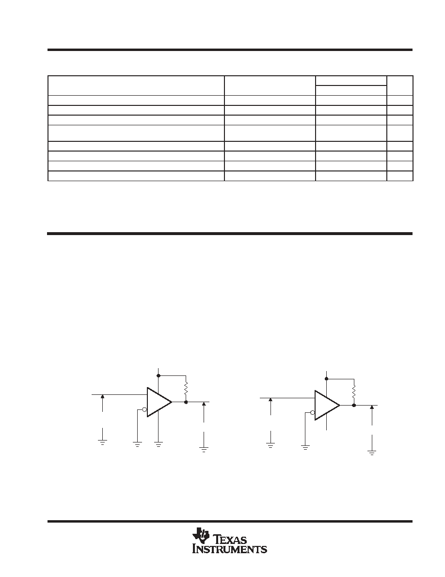
PARAMETER MEASUREMENT INFORMATION
The digital output stage of the TLC372 can be damaged if it is held in the linear region of the transfer curve.
Conventional operational amplifier/comparator testing incorporates the use of a servo loop that is designed to force
the device output to a level within this linear region. Since the servo-loop method of testing cannot be used, the
following alternatives for measuring parameters such as input offset voltage, common-mode rejection, etc., are
offered.
To verify that the input offset voltage falls within the limits specified, the limit value is applied to the input as shown
in Figure 1(a). With the noninverting input positive with respect to the inverting input, the output should be high. With
the input polarity reversed, the output should be low.
A similar test can be made to verify the input offset voltage at the common-mode extremes. The supply voltages can
be slewed as shown in Figure 1(b) for the V
ICR
test, rather than changing the input voltages, to provide greater
accuracy.
5 V
5.1 k
VO
Applied VIO
Limit
VO
5.1 k
1 V
- 4 V
-
+
-
+
(a) VIO WITH VIC = 0
(b) VIO WITH VIC = 4 V
Applied VIO
Limit
Figure 1. Method for Verifying That Input Offset Voltage is Within Specified Limits