
1
Data sheet acquired from Harris Semiconductor
SCHS245B
Features
∑ Buffered Inputs
∑ Typical Propagation Delay
- 4ns at V
CC
= 5V, T
A
= 25
o
C, C
L
= 50pF
∑ Exceeds 2kV ESD Protection per MIL-STD-883,
Method 3015
∑ SCR-Latchup-Resistant CMOS Process and Circuit
Design
∑ Speed of Bipolar FASTTM/AS/S with Significantly
Reduced Power Consumption
∑ Balanced Propagation Delays
∑ AC Types Feature 1.5V to 5.5V Operation and
Balanced Noise Immunity at 30% of the Supply
∑
±
24mA Output Drive Current
- Fanout to 15 FASTTM ICs
- Drives 50
Transmission Lines
Description
The 'AC245 and 'ACT245 are octal-bus transceivers that
utilize Advanced CMOS Logic technology. They are non-
inverting
three-state
bidirectional
transceiver-buffers
intended for two-way transmission from "A" bus to "B" bus or
"B" bus to "A". The logic level present on the direction input
(DIR) determines the data direction. When the output enable
input (OE) is HIGH, the outputs are in the high-impedance
state.
Pinout
CD54AC245, CD54ACT245
(CERDIP)
CD74AC245, CD74ACT245
(PDIP, SOIC, SSOP)
TOP VIEW
Ordering Information
PART
NUMBER
TEMP.
RANGE (
o
C)
PACKAGE
CD54AC245F3A
-55 to 125
20 Ld CERDIP
CD74AC245E
-55 to 125
20 Ld PDIP
CD74AC245M
-55 to 125
20 Ld SOIC
CD74AC245SM
-55 to 125
20 Ld SSOP
CD54ACT245F3A
-55 to 125
20 Ld CERDIP
CD74ACT245E
-55 to 125
20 Ld PDIP
CD74ACT245M
-55 to 125
20 Ld SOIC
CD74ACT245SM
-55 to 125
20 Ld SSOP
NOTES:
1. When ordering, use the entire part number. Add the suffix 96 to
obtain the variant in the tape and reel.
2. Wafer and die for this part number is available which meets all
electrical specifications. Please contact your local TI sales office or
customer service for ordering information.
11
12
13
14
15
16
17
18
20
19
10
9
8
7
6
5
4
3
2
1
DIR
A0
A1
A2
A3
A4
A6
A5
A7
GND
V
CC
B0
B1
B2
OE
B3
B4
B5
B6
B7
September 1998 - Revised October 2000
CAUTION: These devices are sensitive to electrostatic discharge. Users should follow proper IC Handling Procedures.
FASTTM is a Trademark of Fairchild Semiconductor.
Copyright
©
2000, Texas Instruments Incorporated
CD54/74AC245,
CD54/74ACT245
Octal-Bus Transceiver,
Three-State, Non-Inverting
[ /Title
(CD74
AC245
,
CD74
ACT24
5)
/Sub-
ject
(Octal-
Bus
Trans-
ceiver,
Three-
State,
Non-
Invert-
ing)
/Autho
r ()
/Key-
words
(Har-
ris
Semi-
con-
ductor,
Advan
ced
CMOS
, Harris
Semi-
con-
2
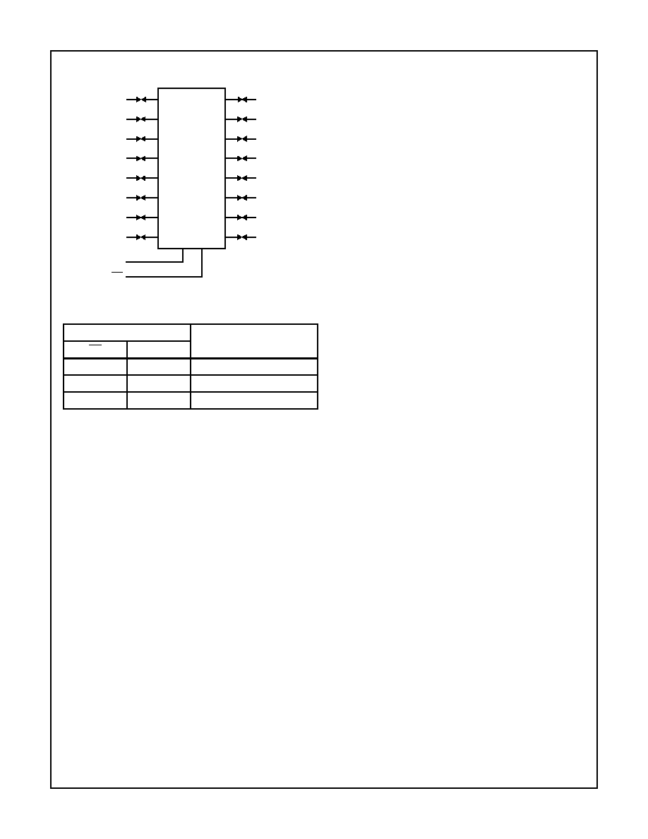
Functional Diagram
TRUTH TABLE
CONTROL INPUTS
OPERATION
OE
DIR
L
L
B Data to A Bus
L
H
A Data to B Bus
H
X
Isolation
H = High Level, L = Low Level, X = Irrelevant
To prevent excess currents in the High-Z (isolation) modes, all I/O
terminals should be terminated with 10k
to 1M
resistors.
18
17
16
15
13
11
12
14
2
B0
B1
B2
B3
B4
B5
B6
B7
OE
DIR
1
19
4
9
3
5
6
7
8
A0
A1
A2
A3
A4
A5
A6
A7
CD54/74AC245, CD54/74ACT245

3
Absolute Maximum Ratings
Thermal Information
DC Supply Voltage, V
CC
. . . . . . . . . . . . . . . . . . . . . . . . -0.5V to 6V
DC Input Diode Current, I
IK
For V
I
< -0.5V or V
I
> V
CC
+ 0.5V
. . . . . . . . . . . . . . . . . . . . . .±
20mA
DC Output Diode Current, I
OK
For V
O
< -0.5V or V
O
> V
CC
+ 0.5V
. . . . . . . . . . . . . . . . . . . .±
50mA
DC Output Source or Sink Current per Output Pin, I
O
For V
O
> -0.5V or V
O
< V
CC
+ 0.5V
. . . . . . . . . . . . . . . . . . . .±
50mA
DC V
CC
or Ground Current, I
CC or
I
GND
(Note 3)
. . . . . . . . .±
100mA
Operating Conditions
Temperature Range, T
A
. . . . . . . . . . . . . . . . . . . . . . -55
o
C to 125
o
C
Supply Voltage Range, V
CC
(Note 4)
AC Types. . . . . . . . . . . . . . . . . . . . . . . . . . . . . . . . . . .1.5V to 5.5V
ACT Types . . . . . . . . . . . . . . . . . . . . . . . . . . . . . . . . .4.5V to 5.5V
DC Input or Output Voltage, V
I
, V
O
. . . . . . . . . . . . . . . . . 0V to V
CC
Input Rise and Fall Slew Rate, dt/dv
AC Types, 1.5V to 3V . . . . . . . . . . . . . . . . . . . . . . . . . 50ns (Max)
AC Types, 3.6V to 5.5V . . . . . . . . . . . . . . . . . . . . . . . . 20ns (Max)
ACT Types, 4.5V to 5.5V. . . . . . . . . . . . . . . . . . . . . . . 10ns (Max)
Thermal Resistance (Typical, Note 5)
JA
(
o
C/W)
E Package . . . . . . . . . . . . . . . . . . . . . . . . . . . . . . . .
69
M Package . . . . . . . . . . . . . . . . . . . . . . . . . . . . . . . .
58
SM Package . . . . . . . . . . . . . . . . . . . . . . . . . . . . . .
70
Maximum Junction Temperature (Plastic Package) . . . . . . . . . . 150
o
C
Maximum Storage Temperature Range . . . . . . . . . .-65
o
C to 150
o
C
Maximum Lead Temperature (Soldering 10s) . . . . . . . . . . . . . 300
o
C
CAUTION: Stresses above those listed in "Absolute Maximum Ratings" may cause permanent damage to the device. This is a stress only rating and operation
of the device at these or any other conditions above those indicated in the operational sections of this specification is not implied.
NOTES:
3. For up to 4 outputs per device, add
±
25mA for each additional output.
4. Unless otherwise specified, all voltages are referenced to ground.
5. The package thermal impedance is calculated in accordance with JESD 51-7.
DC Electrical Specifications
PARAMETER
SYMBOL
TEST
CONDITIONS
V
CC
(V)
25
o
C
-40
o
C TO
85
o
C
-55
o
C TO
125
o
C
UNITS
V
I
(V)
I
O
(mA)
MIN
MAX
MIN
MAX
MIN
MAX
AC TYPES
High Level Input Voltage
V
IH
-
-
1.5
1.2
-
1.2
-
1.2
-
V
3
2.1
-
2.1
-
2.1
-
V
5.5
3.85
-
3.85
-
3.85
-
V
Low Level Input Voltage
V
IL
-
-
1.5
-
0.3
-
0.3
-
0.3
V
3
-
0.9
-
0.9
-
0.9
V
5.5
-
1.65
-
1.65
-
1.65
V
High Level Output Voltage
V
OH
V
IH
or V
IL
-0.05
1.5
1.4
-
1.4
-
1.4
-
V
-0.05
3
2.9
-
2.9
-
2.9
-
V
-0.05
4.5
4.4
-
4.4
-
4.4
-
V
-4
3
2.58
-
2.48
-
2.4
-
V
-24
4.5
3.94
-
3.8
-
3.7
-
V
-75
(Note 6, 7)
5.5
-
-
3.85
-
-
-
V
-50
(Note 6, 7)
5.5
-
-
-
-
3.85
-
V
CD54/74AC245, CD54/74ACT245

4
Low Level Output Voltage
V
OL
V
IH
or V
IL
0.05
1.5
-
0.1
-
0.1
-
0.1
V
0.05
3
-
0.1
-
0.1
-
0.1
V
0.05
4.5
-
0.1
-
0.1
-
0.1
V
12
3
-
0.36
-
0.44
-
0.5
V
24
4.5
-
0.36
-
0.44
-
0.5
V
75
(Note 6, 7)
5.5
-
-
-
1.65
-
-
V
50
(Note 6, 7)
5.5
-
-
-
-
-
1.65
V
Input Leakage Current
I
I
V
CC
or
GND
-
5.5
-
±
0.1
-
±
1
-
±
1
µ
A
Three-State Leakage
Current
I
OZ
V
IH
or V
IL
V
O
= V
CC
or GND
-
5.5
-
±
0.5
-
±
5
-
±
10
µ
A
Quiescent Supply Current
MSI
I
CC
V
CC
or
GND
0
5.5
-
8
-
80
-
160
µ
A
ACT TYPES
High Level Input Voltage
V
IH
-
-
4.5 to
5.5
2
-
2
-
2
-
V
Low Level Input Voltage
V
IL
-
-
4.5 to
5.5
-
0.8
-
0.8
-
0.8
V
High Level Output Voltage
V
OH
V
IH
or V
IL
-0.05
4.5
4.4
-
4.4
-
4.4
-
V
-24
4.5
3.94
-
3.8
-
3.7
-
V
-75
(Note 6, 7)
5.5
-
-
3.85
-
-
-
V
-50
(Note 6, 7)
5.5
-
-
-
-
3.85
-
V
Low Level Output Voltage
V
OL
V
IH
or V
IL
0.05
4.5
-
0.1
-
0.1
-
0.1
V
24
4.5
-
0.36
-
0.44
-
0.5
V
75
(Note 6, 7)
5.5
-
-
-
1.65
-
-
V
50
(Note 6, 7)
5.5
-
-
-
-
-
1.65
V
Input Leakage Current
I
I
V
CC
or
GND
-
5.5
-
±
0.1
-
±
1
-
±
1
µ
A
Three-State or Leakage
Current
I
OZ
V
IH
or V
IL
V
O
= V
CC
or GND
-
5.5
-
±
0.5
-
±
5
-
±
10
µ
A
Quiescent Supply Current
MSI
I
CC
V
CC
or
GND
0
5.5
-
8
-
80
-
160
µ
A
Additional Supply Current per
Input Pin TTL Inputs High
1 Unit Load
I
CC
V
CC
-2.1
-
4.5 to
5.5
-
2.4
-
2.8
-
3
mA
NOTES:
6. Test one output at a time for a 1-second maximum duration. Measurement is made by forcing current and measuring voltage to minimize
power dissipation.
7. Test verifies a minimum 50
transmission-line-drive capability at 85
o
C, 75
at 125
o
C.
DC Electrical Specifications
(Continued)
PARAMETER
SYMBOL
TEST
CONDITIONS
V
CC
(V)
25
o
C
-40
o
C TO
85
o
C
-55
o
C TO
125
o
C
UNITS
V
I
(V)
I
O
(mA)
MIN
MAX
MIN
MAX
MIN
MAX
CD54/74AC245, CD54/74ACT245

5
ACT Input Load Table
INPUT
UNIT LOAD
An, Bn
0.83
OE
0.64
DIR
0.25
NOTE: Unit load is
I
CC
limit specified in DC Electrical Specifications
Table, e.g., 2.4mA max at 25
o
C.
Switching Specifications
Input t
r
, t
f
= 3ns, C
L
= 50pF (Worst Case)
PARAMETER
SYMBOL
V
CC
(V)
-40
o
C TO 85
o
C
-55
o
C TO 125
o
C
UNITS
MIN
TYP
MAX
MIN
TYP
MAX
AC TYPES
Propagation Delay,
Data to Output
t
PLH
, t
PHL
1.5
-
-
96
-
-
106
ns
3.3
(Note 9)
3.2
-
10.8
3
-
11.9
ns
5
(Note 10)
2.2
-
7.7
2.1
-
8.5
ns
Propagation Delay,
Output Disable to Output
t
PLZ
, t
PHZ
1.5
-
-
159
-
-
175
ns
3.3
4.7
-
15.9
4.4
-
17.5
ns
5
3.7
-
12.7
3.5
-
14
ns
Propagation Delay,
Output Enable to Output
t
PZL
, t
PZH
1.5
-
-
159
-
-
175
ns
3.3
5.6
-
19
5.3
-
21
ns
5
3.7
-
12.7
3.5
-
14
ns
Minimum (Valley) V
OH
During
Switching of Other Outputs
(Output Under Test Not Switching)
V
OHV
See Figure 1
5
-
4 at
25
o
C
-
-
4 at
25
o
C
-
V
Maximum (Peak) V
OL
During
Switching of Other Outputs
(Output Under Test Not Switching)
V
OLP
See Figure 1
5
-
1 at
25
o
C
-
-
1 at
25
o
C
-
V
Three-State Output Capacitance
C
O
-
-
15
-
-
15
-
pF
Input Capacitance
C
I
-
-
-
10
-
-
10
pF
Power Dissipation Capacitance
C
PD
(Note 11)
-
-
57
-
-
57
-
pF
ACT TYPES
Propagation Delay,
Data to Output
t
PLH
, t
PHL
5
(Note 10)
2.7
-
9.1
2.5
-
10
ns
Propagation Delay,
Output Disable to Output
t
PLZ
, t
PHZ
5
3.7
12.7
3.5
14
ns
Propagation Delay,
Output Enable to Output
t
PZL
, t
PZH
5
3.8
13.1
3.6
14.4
ns
Minimum (Valley) V
OH
During
Switching of Other Outputs
(Output Under Test Not Switching)
V
OHV
See Figure 1
5
-
4 at
25
o
C
-
-
4 at
25
o
C
-
V
Maximum (Peak) V
OL
During
Switching of Other Outputs
(Output Under Test Not Switching)
V
OLP
See Figure 1
5
-
1 at
25
o
C
-
-
1 at
25
o
C
-
V
CD54/74AC245, CD54/74ACT245