TIBPAL20L8-7C, TIBPAL20R4-7C, TIBPAL20R6-7C, TIBPAL20R8-7C
TIBPAL20L8-10M, TIBPAL20R4-10M, TIBPAL20R6-10M, TIBPAL20R8-10M
HIGH-PERFORMANCE IMPACT-X
TM
PAL
Æ
CIRCUITS
SRPS005D ≠ D3307, OCTOBER 1989 ≠ REVISED NOVEMBER 1995
POST OFFICE BOX 655303
∑
DALLAS, TEXAS 75265
Copyright
©
1995, Texas Instruments Incorporated
1
PRODUCTION DATA information is current as of publication date. Products
conform to specifications per the terms of Texas Instruments standard
warranty. Production processing does not necessarily include testing of all
parameters.
∑
High-Performance Operation:
f
max
(no feedback)
TIBPAL20R' -7C Series . . . 100 MHz
TIBPAL20R' -10M Series . . . 62.5 MHz
f
max
(internal feedback)
TIBPAL20R ' -7C Series . . . 100 MHz
TIBPAL20R ' -10M Series . . . 62.5 MHz
f
max
(external feedback)
TIBPAL20R' -7C Series . . . 74 MHz
TIBPAL20R' -10M Series . . . 50 MHz
Propagation Delay
TIBPAL20L8-7C Series . . . 7 ns Max
TIBPAL20L8-10M Series . . . 10 ns Max
∑
Functionally Equivalent, but Faster Than
Existing 24-Pin PLD Circuits
∑
Preload Capability on Output Registers
Simplifies Testing
∑
Power-Up Clear on Registered Devices (All
Register Outputs are Set Low, but Voltage
Levels at the Output Pins Go High)
∑
Package Options Include Both Plastic and
Ceramic Chip Carriers in Addition to Plastic
and Ceramic DIPs
∑
Security Fuse Prevents Duplication
∑
Dependable Texas Instruments Quality and
Reliability
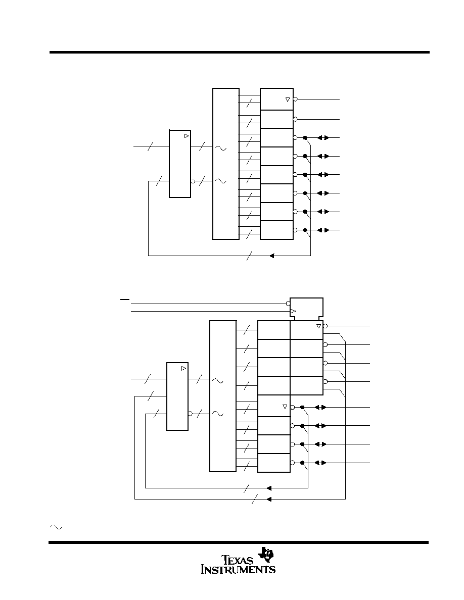
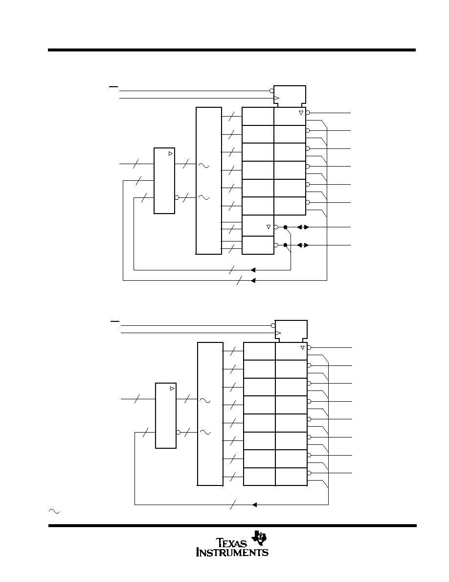
DEVICE
I
INPUTS
3-STATE
O OUTPUTS
REGISTERED
Q OUTPUTS
I/O
PORT
S
PAL20L8
14
2
0
6
PAL20R4
12
0
4 (3-state buffers)
4
PAL20R6
12
0
6 (3-state buffers)
2
PAL20R8
12
0
8 (3-state buffers)
0
description
These programmable array logic devices feature high speed and functional equivalency when compared with
currently available devices. These IMPACT-X
TM
circuits combine the latest Advanced Low-Power Schottky
technology with proven titanium-tungsten fuses to provide reliable, high-performance substitutes for
conventional TTL logic. Their easy programmability allows for quick design of custom functions and typically
results in a more compact circuit board. In addition, chip carriers are available for futher reduction in board
space.
All of the register outputs are set to a low level during power-up. Extra circuitry has been provided to allow loading
of each register asynchronously to either a high or low state. This feature simplifies testing because the registers
can be set to an initial state prior to executing the test sequence.
The TIBPAL20' C series is characterized from 0
∞
C to 75
∞
C. The TIBPAL20' M series is characterized for
operation over the full military temperature range of ≠55
∞
C to 125
∞
C.
These devices are covered by U.S. Patent 4,410,987.
IMPACT-X is a trademark of Texas Instruments Incorporated.
PAL is a registered trademark of Advanced Micro Devices Inc.
1
2
3
4
5
6
7
8
9
10
11
12
24
23
22
21
20
19
18
17
16
15
14
13
I
I
I
I
I
I
I
I
I
I
I
GND
V
CC
I
O
I/O
I/O
I/O
I/O
I/O
I/O
O
I
I
TIBPAL20L8'
C SUFFIX . . . JT OR NT PACKAGE
M SUFFIX . . . JT PACKAGE
(TOP VIEW)
3 2 1 28 27
12 13
5
6
7
8
9
10
11
25
24
23
22
21
20
19
I/O
I/O
I/O
NC
I/O
I/O
I/O
I
I
I
NC
I
I
I
4
26
14 15 16 17 18
I
I
GND
NC
I
I
O
I
I
I
NC
I
O
TIBPAL20L8'
C SUFFIX . . . FN PACKAGE
M SUFFIX . . . FK PACKAGE
(TOP VIEW)
NC
≠
No internal connection
Pin assignments in operating mode
V
CC

TIBPAL20R4-7C, TIBPAL20R6-7C, TIBPAL20R8-7C
TIBPAL20R4-10M, TIBPAL20R6-10M, TIBPAL20R8-10M
HIGH-PERFORMANCE IMPACT-X
TM
PAL
Æ
CIRCUITS
SRPS005D ≠ D3307, OCTOBER 1989 ≠ REVISED NOVEMBER 1995
POST OFFICE BOX 655303
∑
DALLAS, TEXAS 75265
2
CLK
I
I
I
I
I
I
I
I
I
I
GND
I
I/O
I/O
Q
Q
Q
Q
I/O
I/O
I
1
2
3
4
5
6
7
8
9
10
11
12
24
23
22
21
20
19
18
17
16
15
14
13
VCC
OE
TIBPAL20R4'
C SUFFIX . . . JT OR NT PACKAGE
M SUFFIX . . . JT PACKAGE
(TOP VIEW)
I
I
GND
NC
I
I/O
I
I
CLK
NC
I
I/O
(TOP VIEW)
V
CC
11
19
12 13 14 15 16 17 18
4
10
9
8
7
6
5
I/O
20
21
22
23
24
25
3 2 1 28 27 26
I
I
I
NC
I
I
I
Q
Q
NC
Q
Q
I/O
TIBPAL20R4'
C SUFFIX . . . FN PACKAGE
M SUFFIX . . . FK PACKAGE
NC
≠
No internal connection
OE
CLK
I
I
I
I
I
I
I
I
I
I
GND
I
I/O
Q
Q
Q
Q
Q
Q
I/O
I
1
2
3
4
5
6
7
8
9
10
11
12
24
23
22
21
20
19
18
17
16
15
14
13
OE
I
I
GND
NC
I
I/O
I
I
CLK
NC
I
I/O
V
CC
11
19
12 13 14 15 16 17 18
4
10
9
8
7
6
5
Q
20
21
22
23
24
25
3 2 1 28 27 26
I
I
I
NC
I
I
I
Q
Q
NC
Q
Q
Q
OE
VCC
(TOP VIEW)
TIBPAL20R6'
C SUFFIX . . . JT OR NT PACKAGE
M SUFFIX . . . JT PACKAGE
(TOP VIEW)
TIBPAL20R6'
C SUFFIX . . . FN PACKAGE
M SUFFIX . . . FK PACKAGE
CLK
I
I
I
I
I
I
I
I
I
I
GND
I
Q
Q
Q
Q
Q
Q
Q
Q
I
1
2
3
4
5
6
7
8
9
10
11
12
24
23
22
21
20
19
18
17
16
15
14
13
OE
I
I
GND
NC
I
Q
I
I
CLK
NC
I
Q
V
CC
11
19
12 13 14 15 16 17 18
4
10
9
8
7
6
5
Q
20
21
22
23
24
25
3 2 1 28 27 26
I
I
I
NC
I
I
I
Q
Q
NC
Q
Q
Q
OE
VCC
(TOP VIEW)
TIBPAL20R8'
C SUFFIX . . . JT OR NT PACKAGE
M SUFFIX . . . JT PACKAGE
(TOP VIEW)
TIBPAL20R8'
C SUFFIX . . . FN PACKAGE
M SUFFIX . . . FK PACKAGE
Pin assignments in operating mode
4
8
12
16
20
24
28
32
I
3
I
4
I
5
I
6
I
7
I
8
I
9
I
10
O
22
I/O
21
I/O
20
I/O
19
I/O
18
I/O
17
I/O
16
O
15
I
14
Increment
I
1
Fuse number = First fuse number + Increment
Pin numbers shown are for JT and NT packages.
0
40
80
120
160
200
240
280
320
360
400
440
480
520
560
600
640
680
720
760
800
840
880
920
960
1000
1040
1080
1120
1160
1200
1240
1280
1320
1360
1400
1440
1480
1520
1560
1600
1640
1680
1720
1760
1800
1840
1880
1920
1960
2000
2040
2080
2120
2160
2200
2240
2280
2320
2360
2400
2440
2480
2520
First Fuse
Numbers
36
39
0
I
2
I
23
I
11
I
13
TIBPAL20L8-7C
TIBPAL20L8-10M
HIGH-PERFORMANCE IMPACT-X
TM
PAL
Æ
CIRCUITS
SRPS005D ≠ D3307, OCTOBER 1989 ≠ REVISED NOVEMBER 1995
POST OFFICE BOX 655303
∑
DALLAS, TEXAS 75265
5
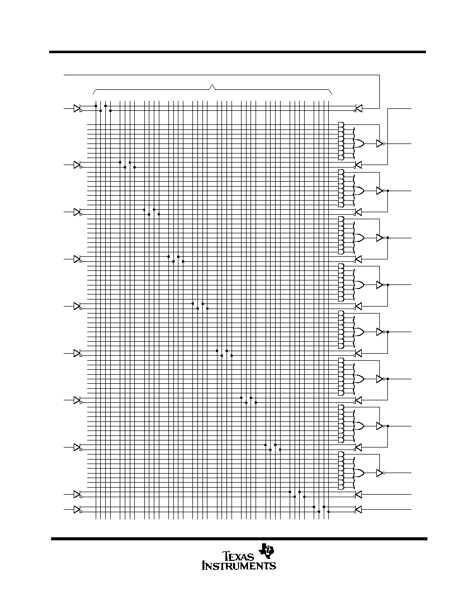
logic diagram (positive logic)